

FULLY INTEGRATED STEPPER MOTOR DRIVER
■
OPERATING SUPPLY VOLTAGE FROM 8 TO 52V
■ 5A PEAK CURRENT (2.8A DC)
■
R
DS(ON)
■
BUILT-IN DECODING LOGIC
■
BUILT-IN CONSTANT OFF-TIME PWM
CURRENT CONTROL
■
FAST/SLOW DECAY MODE SELECTION
■
HIGH SIDE OVER CURRENT PROTECTION
5.6A TYP.
■
CROSS CONDUCTION PROTECTION
■
THERMAL SHUTDOWN
■ OPERATING FREQUENCY UP TO 100KHz
■
INTRINSIC FAST FREE WHEELING DIODES
■
UVLO: UNDER VOLTAGE LOCKOUT
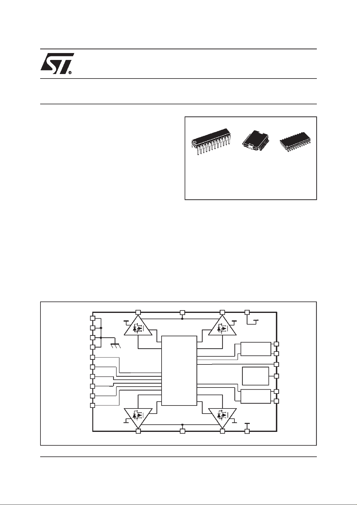
DESCRIPTION
The L6208 is a fully integrated stepper motor driver
manufactured with multipower BCD technology,
which combines isolated DMOS power transistors
with CMOS and bipolarcircuits on the same chip.
0.3Ω TYP. VALUE @ Tj=25°C
L6208
PRELIMINARY DATA
PowerDIP24 PowerSO36 SO24
(20+2+2) (20+2+2)
ORDERING NUMBERS:
L6208N L6208PD L6208D
The logic inputs are CMOS/TTL and µP compatible.
The device also includes all the circuitry needed to
drive a stepper motor, that is the constant off time
PWM control that performs the chopping current control and the state machine that generates the stepping sequence. Other features are the protection of
the high side switches against unsafe over current
conditions and the thermal shutdown.
The L6208 is assembled in PowerDIP24(20+2+2),
PowerSO36 and SO24(20+2+2) packages.
BLOCK DIAGRAM
OUT2
OUT2
V
A
B
SA
V
V
SB
V
SB
SA
PWM
Charge
Pump
PWM
V
A
B
RC
V
V
V
RC
ref A
A
BOOT
CP
ref B
B
VSAVSA
V
SB
GND
GND
GND
GND
EN
Reset
Clock
CW/CCW
HALF/FULL
Control
VSB
OUT1
OUT1
A
B
SENSE
Logic
&
Drivers
SENSE
A
B
January 2001
This ispreliminary information on a new product now in development or undergoing evaluation. Details are subject to change without notice.
1/15
L6208
FUNCTIONAL BLOCK DIAGRAM
CONTROL
HALF/FULL
Clock
RESET
CW/CCW
RCA
VrefA
RCB
VrefB
Vboot
10V
Decoding
Logic
Voltage
Regulator
5V
Current
Detection
Vboot
Over
Thermal
Protection
EN
Input
Interface
Charge
Pump
VCP
Vboot
10V
One Shot
Masking
Time
Vboot
10V
Sense
Comparator
VSA
OUT1A
OUT2A
SENSE A
PWM
BRIDGE A
VSB
BRIDGE B
OUT1B
OUT2B
SENSE B
ABSOLUTE MAXIMUM RATINGS
Symbol Parameter Test conditions Value Unit
V
V
IN,VEN
V
refA,VrefB
V
RCA,RCB
V
SENSE
V
BOOT
I
S(peak)
I
S
V
OD
T
stg,TOP
Supply Voltage 60 V
S
Input and Enable Voltage Range -0.3 to +7 V
Voltage Range at V
Voltage Range atRCAand RC
pins -0.3 to +7 V
ref
B
-0.3 to +7 V
pins
DC Sensing Voltage Range -1 to +4 V
Bootstrap Peak Voltage VS+10 V
Pulsed Supply Current (foreach
V
pin), internally limited by the
S
< 1ms 7.1 A
t
PULSE
overcurrent protection.
DCvSupply Current (foreach V
S
2.8 A
pin)
Differential Voltage Between
60 V
VSA,OUT1A,OUT2A,SENSEAand
VSB, OUT1B, OUT2B, SENSE
Storage and Operating
B
-40 to 150 °C
Temperature Range
2/15
RECOMMENDED OPERATING CONDITIONS
Symbol Parameter MIN MAX Unit
L6208
V
V
OD
Supply Voltages 12 52 V
S
Differential Voltage Between
VSA, OUT1A,OUT2A,SENSEAand
VSB, OUT1B, OUT2B, SENSE
V
SENSE
Sensing voltage
(pulsed tw<t
V
I
OUT
ref
T
f
c
V
Operating Voltage -0.1 5
ref
DC Output Current 2.8 V
Operating Junction Temperature -25 +125 °C
j
Commutation Frequency 100 kHz
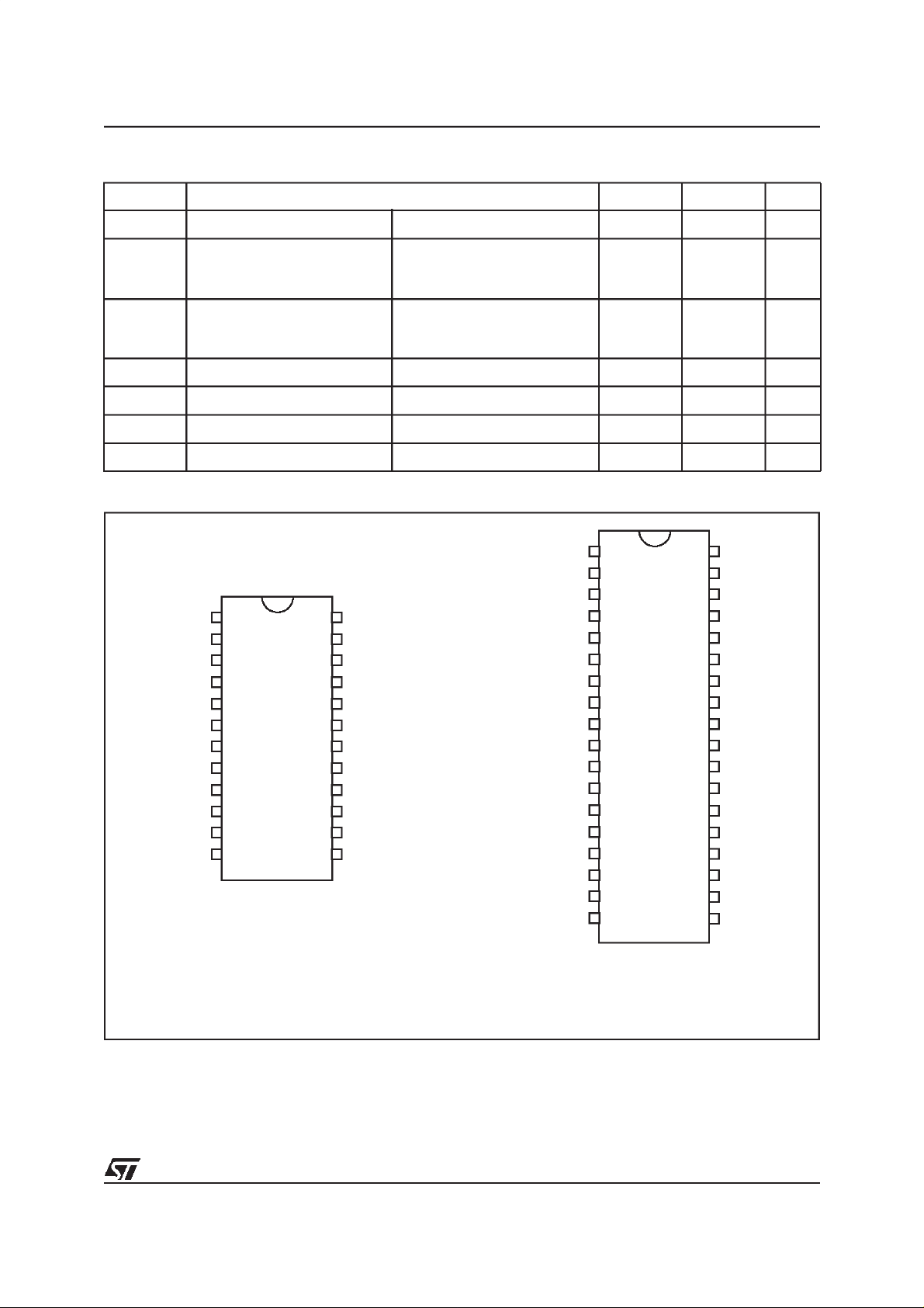
PIN CONNECTIONS(Top View)
RC
RC
V
refB
1
2
3
A
4
A
5
A
6
7
8
B
9
B
10
B
11
12
24
23
22
21
20
19
18
17
16
15
14
13
Clock
CW/CCW
SENSE
OUT1
GND
GND
OUT1
SENSE
HALF/FULL
B
)
rr
(DC)
V
refA
Reset
V
CP
OUT2
V
SA
GND
GND
V
SB
OUT2
V
BOOT
EN
Control
52 V
-6
-1
GND
OUT2
A
Reset
V
Clock
CW/CCW
B
SENSE
OUT1
GND
NC
NC
V
NC
V
refA
RC
NC
NC
NC
SA
CP
1
2
3
4
5
A
6
7
8
9
10
11
12
A
13
A
14
15
A
16
17
18
36
35
34
33
32
31
30
29
28
27
26
25
24
23
22
21
20
19
6
1
GND
NC
NC
V
SB
OUT2
B
NC
V
BOOT
EN
Control
HALF/FULL
V
refB
SENSE
RC
B
B
NC
OUT1
B
NC
NC
GND
V
V
PDIP24/SO24 PowerSO36
3/15
L6208
PIN DESCRIPTION
Name PowerSO36
PDIP24/
SO24
Function
V
SA
V
SB
OUT1
A
OUT2
A
OUT1
B
OUT2
B
SENSE
SENSE
A
B
GND 1, 18, 19, 36 6, 7,
4 20 Supply voltage of the bridge A.
33 17 Supply voltage of the bridge B. Must be connected to VSA.
15
5
22
32
21
16
5
8
Bridge A outputs.
Bridge B outputs.
12 3 Sense resistor for the bridge A.
25 10 Sense resistor for the bridge B.
Common ground terminals. In Powerdip and SO packages, these pins
18, 19
are also used for heat dissipation toward the PCB.
EN 29 14 Chip Enable. A Low logic level applied to this pin switches Off all the
power DMOSs.
HALF/FULL 27 12 Logic input. When high, HALF STEP operation is selected; a Low logic
level selects FULL STEP operation.
ONE-PHASE-ON FULL STEPMODE (
selecting FULLwhen the state machine is at an
TWO-PHASE-ON FULL STEPMODE (
selecting FULLwhen the state machine is at an
Reset 8 23 Logic input. A Low logic levelrestores the
wave mode
even
normal mode
odd
home
state (state 1) on the
) is obtained by
numbered state.
) is obtained by
numbered state.
state machine.
Clock 10 1 Logic input. Step Clock. The step occurs on the rising edge of this signal.
CW/CCW 11 2 Logic input. Logic High sets clockwise direction. Logic Low sets
counterclockwise direction.
Control 28 13 Logic input. Selects chopping style. FAST DECAY is selected with logic
Low. A logic High selects SLOW DECAY.
V
ref A
9 24 A voltage applied to these pins sets the reference voltage of the sense
comparators, determining the output current in PWM current control.
V
V
V
BOOT
RC
ref B
CP
A
26 11
7 22 Bootstrap oscillator. Oscillator output forthe external charge pump.
30 15 Supply voltage to overdrive the upper DMOSs.
13 4 A parallel RC network connected tothese pins sets the OFF time of the
low-side power DMOS of the correspondent bridge. The pulse generator
RC
B
24 9
is a monostable triggered by the output of the sense comparator of the
bridge (t
= 0.69 RC).
OFF
4/15
THERMAL DATA
Symbol Description PDIP24 SO24 PowerSO36 Unit
L6208
R
th-j-pins
MaximumThermal Resistance
18 14 -
C/W
°
Junction-Pins
R
th-j-case
Maximum Thermal Resistance
-- 1°C/W
Junction-Case
R
th-j-amb1
R
th-j-amb2
<(1)>Mounted on a multiplayer PCB with a dissipating copper surface on the bottom side of 2 x 12mm x 25mm (with athickness of
<(2)>It’s the same condition of the point above, without any heatsinking surface on the board.
MaximumThermal Resistance
Junction-Ambient
Maximum Thermal Resistance
Junction-Ambient
at least 35 µm).
(1)
(2)
42 50 35 °C/W
58 77 62 °C/W
ELECTRICAL CHARACTERISTICS
(T
=25°C, Vs= 48V, unless otherwise specified)
amb
Symbol Parameter Test Conditions Min Typ Max Unit
V
Output DMOS Transistors
I
DSS
R
DS(ON)
Source Drain Diodes
Supply Voltage 8 52 V
S
I
Quiescent Supply Current All Bridges OFF 5.5 10 mA
S
T
Thermal Shutdown Temperature 150 °C
j
Leakage Current VS= 52V 1 mA
High-side Switch ON Resistance Tj=25°C 0.34 0.4
T
=125°C 0.53 0.59
j
Low-side SwitchON Resistance T
=25°C 0.28 0.34
j
T
=125°C 0.47 0.53
j
Ω
Ω
Ω
Ω
V
Forward ON Voltage ISD= 2.8A, EN = LOW 1.2 1.4 V
SD
t
Reverse Recovery Time If= 2.8A 300 ns
rr
t
Forward Recovery Time 200 ns
fr
Switching Rates
t
D(on)
Output to out Turn ON Delay
Time
t
ON
Output Rise Time
t
D(OFF)
Enable to out Turn OFF Delay
Time
t
OFF
t
DCLK
Output FallTime
Clock to output delay time
(3)
(3)
(3)
(3)
(3)
I
=2.8A 110 250 400 ns
LOAD
I
=2.8A 20 105 300 ns
LOAD
I
=2.8A 240 580 760 ns
LOAD
I
=2.8A 20 78 300 ns
LOAD
I
=2.8A 2 µs
LOAD
5/15

L6208
ELECTRICAL CHARACTERISTICS
(T
=25°C, Vs= 48V, unless otherwise specified)
amb
(continued)
Symbol Parameter Test Conditions Min Typ Max Unit
t
Dead Time Protection 1
dt
t
blank
InternalBlanking Timeon SENSE
1 1.5 µs
pins
f
Charge pump frequency 0.75 1 MHz
CP
UVLO comp
V
th(ON)
V
th(OFF)
TurnON threshold 6.6 7 7.4 µs
TurnOFF threshold 5.6 6 6.4 µs
Logic Input
V
V
I
INH
I
t
CLK
t
RCLK
Low levellogic input voltage -0.3 0.8 V
INL
High levellogic input voltage 2 7 V
INH
High levellogic input current V
Low levellogic input current V
INL
Minimum clock time
t
S
Minimum set up time
t
H
Minimum hold time
t
R
Minimum reset time
(4)
Minimum reset to clockdelay
(4)
(4)
(4)
(4)
=5V 70 µA
IN, EN
= GND -10 µA
IN, EN
see Fig. 2 0.1 1 µs
1 µs
1 µs
1 µs
1 µs
s
µ
Over Current Protection
I
S OVER
Input supply over current
protection threshold
V
DIAG
Open drain low level output
voltage
Comparator and Monostable
I
RCA,RCB
V
Source current at RC pins VRC=2.5 V 3 5 mA
Input common mode comparator
ref
voltage range
V
Comparator threshold voltage on
th
SENSE pins
t
prop
t
OFF
I
bias
TurnOFF propagation delay
PWMRecirculation time
Input bias current at V
<(3)>Resistive load used. See Fig. 1.
<(4)>See Fig. 2.
<(5)>Defined as the time between the voltage at the input of the current sense reaching theV
switch beginning to turn off. The voltage at SENSE pin is increased instantaneously from V
Tj =25 °C 4 5.6 7.1 A
I = 4 mA 0.4 V
-0.1 5 V
V
(5)
V
20 kΩ <R<100kΩ
= 0.5 V V
ref A, B
= 0.5 V 0.1 0.2 0.3 µs
ref A, B
- 5mV V
ref
0.67RC 0.69RC 0.71RC s
ref
+ 5mV
0.1 nF < C < 100 nF
pins 0.2 µA
ref
threshold and the lower DMOS
ref
-10mVtoV
ref
+10 mV.
ref
6/15

Figure 1. Switching Rates Definition
En
50%
L6208
I
OUT
90%
10%
CLK
t
50%
I
OUT
Figure 2. MinimumTiming Definition
D(OFF)tOFF
t
DCLK
t
D(ON)t(ON)
t
t
t
t
CLOCK
CLOCK
Logic Inputs
RESET
t
CLK
t
CLK
t
S
t
R
t
RCLK
t
H
7/15

L6208
Figure 3. Typical Quiescent Currentvs. Supply
Voltage
Iq [mA]
5.6
5.4
5.2
5.0
4.8
4.6
0 102030405060
fc= 1kHz Tj=25°C
[V]
V
S
=85°C
T
j
T
j
= 125°C
Figure 4. Normalized Typical Quiescent
Current vs. Switching Frequency
Iq / (Iq @ 1 kHz)
1.7
1.6
1.5
1.4
1.3
1.2
1.1
1.0
0.9
0 20406080100
f
[kHz]
SW
Figure 6. Typical High-Side RDS(ON) vs.
Supply Voltage
R
[Ω]
DS(ON)
0.380
0.376
0.372
0.368
0.364
0.360
0.356
0.352
0.348
0.344
0.340
0.336
0 5 10 15 20 25 30
Figure 7. Normalized R
Tj=25°C
V
[V]
S
DS(ON)
vs.Junction
Temperature (typical value)
R
/(R
DS(ON)
1.8
1.6
1.4
1.2
1.0
0.8
0 20 40 60 80 100 120 140
DS(ON)
@25°C)
Tj [°C]
Figure 5. Typical Low-Side R
DS(ON)
Voltage
[Ω]
R
DS(ON)
0.300
0.296
Tj=25°C
0.292
0.288
0.284
0.280
0.276
0 5 10 15 20 25 30
8/15
[V]
V
S
vs. Supply
Figure 8. Typical Drain-Source Diode Forward
ON Characteristic
ISD[A]
3.0
Tj=25°C
2.5
2.0
1.5
1.0
0.5
0.0
700 800 900 1000 1100 1200 1300
VSD[mV]

L6208
CIRCUITDESCRIPTION
The L6208 isafully integrated bipolar stepper motor driver withtwo full bridge having power DMOS with atypical
RDSON of 0.3
as a constant T
The decoding logic generates three different sequences, selected by the HALF/FULL input. These are normal
(two phases ), wave drive (one phase energized) and half-step (alternately one phase/two phases energized).
The decoding logic generates three different sequences, selected by the HALF/FULL input. These are normal
(two phases energized), wave drive (one phase energized) and half-step (alternately one phase/two phases energized).
The constant T
When the current in each phase of the motor reaches the value set by the correspondentV
it will be forced to decrease for a constant Toff time, set by the RC network applied to the RCAand RCBpins. If the
Control pin isat a High logiclevel, duringthe off-time the voltageapplied to the motorphase willbe approx.0 V,turning
on the high-side MOSFETs of the bridge (slow decayrecirculation); if control is Low, instead, the voltage applied to
the phase will be reversed, turning off the low side MOSFET that was on and turning on the opposite low-side (fast
decay recirculation).
Figure 9.
Ω each. All the circuitry to implement the phase generation (decoding logic)is integrated, as well
PWM control for the current, separately for any of the two winding of the driven motor.
off
PWM current control consists ina sense comparator and a monostable.
off
voltage(V
ref
ref/RSENSE
),
V
S
On Time
Slow-Decay
Figure 10. PWM Chopping Current Control
I
OUT
T
ON
V
ref/RSENSE
Threshold
V
S
Off Time in
Recirculation
Off Time in
Fast-Decay
V
S
Recirculation
T
OFF
(Recirculation)
t
9/15

L6208
A non-dissipative current sensing on the high side power DMOSs, an internal reference and an internal open
drain, with a pull down capability of 4mA (typical value), that goes LOW under fault conditions, ensure a protection against short circuit to GND or between two phases of each of the two full bridges. The trip point of this
protection is internally set at 5.6 A (typ. value). By using an external R-C on the EN pins, the off time before
recover normaloperation conditions after a fault can be easily programmed, by means of the accuratethreshold
of the logic inputs. Note that protection against short to the supply rail is typically provided by the PWM current
control circuitry.
These features make the L6208 a complete bipolar stepper motor driver that outperforms the components currently available on the market
MOTOR DRIVING PHASE SEQUENCE
The decoding logic integrated in the L6208 generates thesequences for normal drive, wave drive and half step
modes. The state machine sequences and the output currents (neglecting, for simplicity, the PWM control) are
shown below, in the case of clockwise rotation. For counterclockwise rotation the sequences are simply reversed. The state machine advances on the rising edge of the Clock signal, and a Low logic level on the Reset
input restores the logic to state 1.
HALF STEP MODE
Half step mode is selected by a high logic level on the HALF/FULL pin.
Figure 11.
345
2
1
6
78
I
OUT1A
I
OUT2A
I
OUT1B
I
OUT2B
Clock
81234567
10/15

L6208
NORMALDRIVE MODE
(Full-step two-phase-on)
Normal drive mode is selected by a Low level on the HALF/FULL input when the state machine is at an odd
numbered state.
Figure 12.
I
OUT1A
I
OUT2A
345
2
1
6
78
I
OUT1B
I
OUT2B
Clock
71357135
WAVEDRIVE MODE
(Full-step one-phase-on)
Wave drive mode is selected by a Low level on the HALF/FULL input when the state machine is at an even
numbered state.
Figure 13.
I
OUT1A
345
I
OUT2A
2
1
6
78
I
OUT1B
I
OUT2B
Clock
82468246
11/15

L6208
DIM.
MIN. TYP. MAX. MIN. TYP.
A 4.320
A1 0.380
A2 3.300
B 0.410 0.460 0.510 0.016 0.018
mm inch
MAX.
0.170
0.015
0.130
0.020
B1 1.400 1.520 1.650 0.055 0.060 0.06
c 0.200 0.250 0.300 0.008 0.010
D 31.62 31.75 31.88 1.245 1.250 1.255
E 7.620 8.260 0.300
e 2.54
0.100
0.012
0.325
E1 6.350 6.600 6.860 0.250 0.260 0.27
e1
L 3.180 3.430 0.125
7.620
M0°min, 15°
max.
0.300
0.135
OUTLINE AND
MECHANICAL DATA
5
0
Powerdip 24
E1
A2
A
13
12
A1
SDIP24L
e1
c
M
L
B
D
24
1
B1
e
12/15

L6208
DIM.
MIN. TYP. MAX. MIN. TYP. MAX.
A 2.35 2.65 0.093 0.104
A1 0.10 0.30 0.004 0.012
A2 2.55 0.100
B 0.33 0.51 0.013 0.0200
C 0.23 0.32 0.009 0.013
D 15.20 15.60 0.598 0.614
E 7.40 7.60 0.291 0.299
e 1.27 0,050
H 10.0 10.65 0.394 0.419
h 0.25 0.75 0.010 0.030
k0°(min.),8° (max.)
L 0.40 1.27 0.016 0.050
mm inch
OUTLINEAND
MECHANICAL DATA
SO24
0.10mm
.004
Seating Plane
1
A2
A
Be
A1
K
D
1324
E
12
hx45°
L
A1 C
H
SO24
13/15

L6208
DIM.
MIN. TYP. MAX. MIN. TYP. MAX.
mm inch
A 3.60 0.141
a1 0.10 0.30 0.004 0.012
a2 3.30 0.130
a3 0 0.10 0 0.004
b 0.22 0.38 0.008 0.015
c 0.23 0.32 0.009 0.012
D (1) 15.80 16.00 0.622 0.630
D1 9.40 9.80 0.370 0.385
E 13.90 14.50 0.547 0.570
e 0.65 0.0256
e3 11.05 0.435
E1 (1) 10.90 11.10 0.429 0.437
E2 2.90 0.114
E3 5.80 6.20 0.228 0.244
E4 2.90 3.20 0.114 0.126
G 0 0.10 0 0.004
H 15.50 15.90 0.610 0.626
h 1.10 0.043
L 0.80 1.10 0.031 0.043
N10°(max.)
S8°(max.)
(1):”D” and”E1” donot include mold flash or protrusions
- Moldflash or protrusionsshall not exceed0.15mm(0.006 inch)
- Criticaldimensionsare”a3”, ”E” and ”G”.
OUTLINE AND
MECHANICALDATA
PowerSO36
E2
hx45°
NN
a2
A
1936
0.12 A B
⊕
e
E1
M
DETAIL A
118
A
e3
H
D
b
DETAIL B
lead
a3
B
Gage Plane
PSO36MEC
BOTTOM VIEW
DETAIL B
0.35
S
L
c
a1
E
DETAIL A
slug
E3
D1
-C-
SEATING PLANE
GC
(COPLANARITY)
14/15

L6208
Information furnished is believed tobe accurate and reliable. However,STMicroelectronics assumes no responsibility for the consequences
of useof such information nor for any infringementof patents or other rightsof third partieswhich may result from its use. No license is granted
by implication or otherwise under any patent or patent rights of STMicroelectronics. Specifications mentioned in this publication are subject
to change without notice. This publication supersedes and replaces all information previously supplied. STMicroelectronics products arenot
authorized for use as critical components in life support devices or systems without express written approval of STMicroelectronics.
The ST logo is a registered trademark of STMicroelectronics
2001 STMicroelectronics - All Rights Reserved
Australia - Brazil - China - Finland - France - Germany - Hong Kong - India - Italy - Japan - Malaysia - Malta- Morocco - Singapore - Spain
STMicroelectronics GROUP OF COMPANIES
- Sweden- Switzerland - United Kingdom - U.S.A.
http://www.st.com
15/15
 Loading...