

DMOS DUAL FULL BRIDGE DRIVER
■
OPERATING SUPPLY VOLTAGE FROM 8 TO 52V
■ 5.6A OUTPUT PEAK CURRENT (2.8A DC)
■ R
■ OPERATING FREQUENCY UP TO 100KHz
■
PROGRAMMABLE HIGH SIDE OVERCURRENT
DETECTION AND PROTECTION
■
DIAGNOSTIC OUTPUT
■
PARALLE LED OPERATION
■ CROSS CONDUCTION PROTECTION
■ THERMAL SHUTDOWN
■ UNDER VOLTAGE LOCKOUT
■
INTEGRATED FAST FREE WHEELING DIODES
0.3Ω TYP. VA LUE @ Tj = 25 °C
DS(ON)
PowerDIP24
(20+2+2)
PowerSO36
ORDERING NUMBERS:
L6206N (PowerDIP24)
L6206PD (PowerSO36)
L6206D (SO24)
L6206
SO24
(20+2+2)
TYPICAL APPLICATIONS
■ BIPOLAR STEPPER MOTOR
■ DUAL OR QUAD DC MOTOR
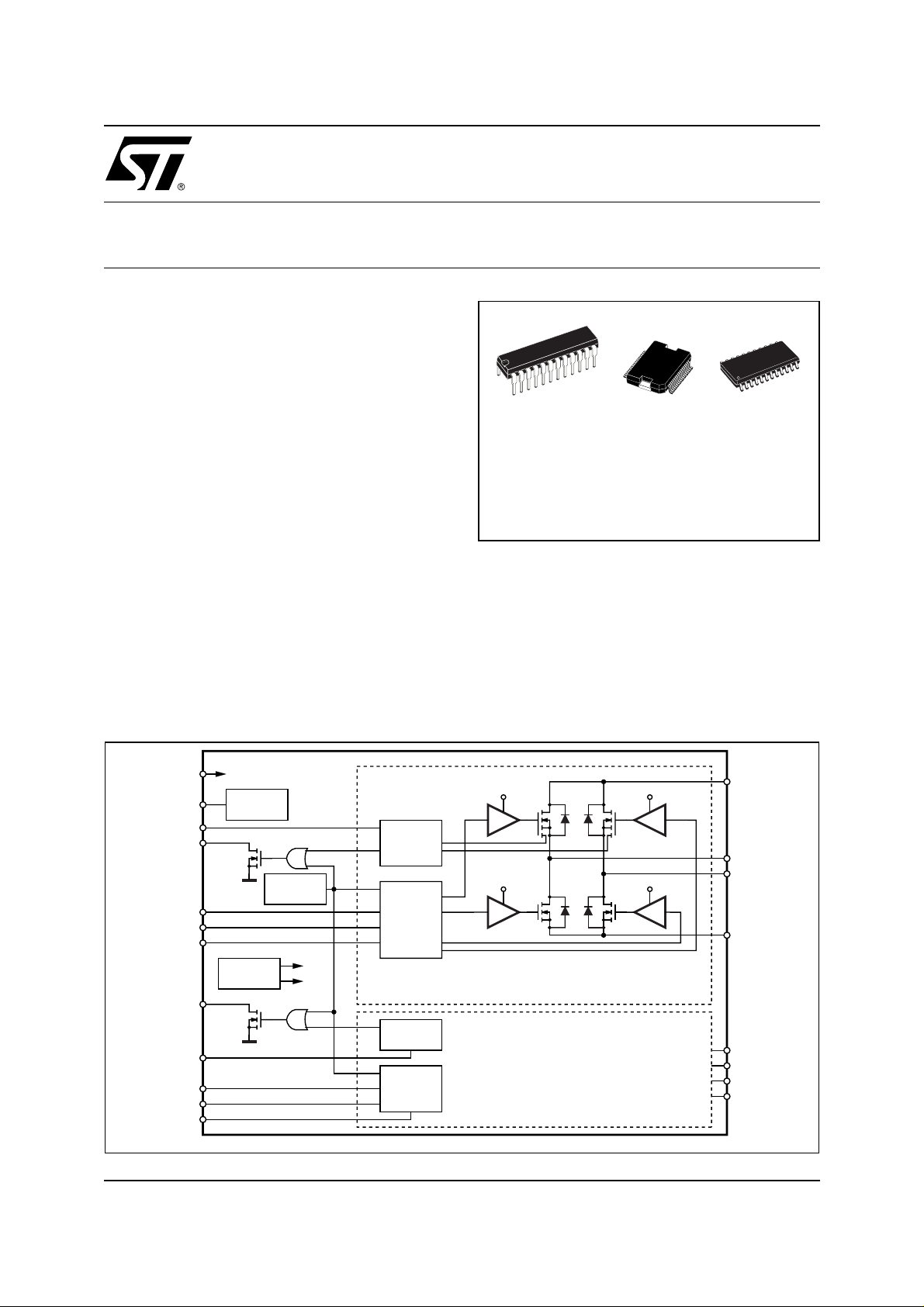
DESCRIPTION
The L6206 is a DMOS Dual Full Bridge designed for
motor control applications, realized in MultiPower-
BLOCK DIAGRAM
VBOOT
VCP
PROGCL
OCD
EN
IN1
IN2
OCD
PROGCL
EN
IN1
IN2
A
A
A
A
A
B
B
B
B
B
V
BOOT
CHARGE
PUMP
VOLTAGE
REGULA TOR
OCD
THERMAL
PROTECTION
10V
5V
OCD
OVER
A
B
CURRENT
DETECTION
GA TE
LOGIC
OVER
CURRENT
DETECTION
GA TE
LOGIC
BCD technology, which combines isolated DMOS
Power Transistors with CMOS and bipolar c ir cuits on
the same chip. Available in PowerDIP24 (20+2+2),
PowerSO36 and SO24 (20+2+2) packages, the
L6206 features thermal shutdown and a non-dis sipative overcurrent detection on the high side Power
MOSFETs plus a diagnostic output that can be easily
used to implement the overcurrent protection.
VS
V
BOOT
10V 10V
V
BOOT
BRIDGE A
BRIDGE B
D99IN1088A
A
OUT1
OUT2
SENSE
V
S
B
OUT1
OUT2
SENSE
A
A
A
B
B
B
September 2003
1/23

L6206
ABSOLUTE MAXIMUM RATINGS
Symbol Parameter Test conditions Value Unit
V
V
OD
Supply Voltage
S
Differential Voltage between
VSA, OUT1A, OUT2A, SENSEA and
VSB, OUT1B, OUT2B, SENSE
VSA =
VSB = V
VSA =
VSB = VS = 60V;
V
SENSEA
B
= V
S
SENSEB
= GND
60 V
60 V
OCDA,OCDBOCD pins Voltage Range -0.3 to +10 V
PROGCLA,
PROGCL
V
BOOT
V
IN,VEN
V
SENSEA,
V
SENSEB
I
S(peak)
PROGCL pins Voltage Range -0.3 to +7 V
B
Bootstrap Peak Voltage
VSA =
VSB = V
S
VS + 10 V
Input and Enable Voltage Range -0.3 to +7 V
Voltage Range at pins SENSEA
and SENSE
B
Pulsed Supply Current (for each
pin), internally limited by the
V
S
VSA =
t
PULSE
VSB = VS;
< 1ms
-1 to +4 V
7.1 A
overcurrent protection
I
S
T
, T
stg
RMS Supply Current (for each
pin)
V
S
Storage and Operating
OP
VSA =
VSB = V
S
2.8 A
-40 to 150 °C
Temperature Range
RECOMMENDED OPERATING CONDITIONS
Symbol Parameter Test Conditions MIN MAX Unit
V
S
V
OD
V
SENSEA,
V
SENSEB
I
OUT
T
j
f
sw
Supply Voltage
Differential Voltage Between
VSA, OUT1A, OUT2A, SENSEA and
VSB, OUT1B, OUT2B, SENSE
Voltage Range at pins SENSEA
and SENSE
B
RMS Output Current 2.8 A
Operating Junction Temperature -25 +125 °C
Switching Frequency 100 KHz
VSA =
VSA =
V
SENSEA
B
(pulsed tW < trr)
(DC)
VSB = V
VSB = VS;
= V
SENSEB
S
852V
52 V
-6
-1
6
1
V
V
2/23

L6206
THERMA L D ATA
Symbol Description PowerDIP24 SO24 PowerSO36 Unit
R
th-j-pins
R
th-j-case
R
th-j-amb1
R
th-j-amb1
R
th-j-amb1
R
th-j-amb2
(1) Mounted on a multi-layer FR4 PCB with a dissipati ng copper surface on the bottom side of 6 cm2 (with a thickness of 35 µm) .
(2) Mounted on a multi-layer FR4 PCB with a dissipati ng copper surface on the top side of 6 cm2 (with a thickness of 35 µm) .
(3) Mounted on a multi-layer FR4 PCB with a dissipating copper surface on the top side of 6 cm2 (with a thickness of 35 µm), 16 via holes
and a groun d l ayer.
(4) Mounted on a multi-layer FR4 PCB without any hea t s i nking surfac e on the board.
PIN CONNECTIONS (Top View)
MaximumThermal Resistance Junction-Pins 18 14 - °C/W
Maximum Thermal Resistance Junction-Case - - 1 °C/W
MaximumThermal Resistance Junction-Ambient
Maximum Thermal Resistance Junction-Ambient
MaximumThermal Resistance Junction-Ambient
Maximum Thermal Resistance Junction-Ambient
1
2
3
4
43 51 - °C/W
--35°C/W
--15°C/W
58 77 62 °C/W
IN1
IN2
SENSE
OCD
OUT1
GND
GND
OUT1
OCD
SENSE
IN1
IN2
1
A
2
A
3
A
4
A
5
A
6
7
8
B
9
B
10
B
11
B
12
B
D99IN1089A
24
PROGCL
EN
VCP
OUT2
VS
A
A
A
A
23
22
21
20
GND19
GND
18
VS
17
16
15
14
13
B
OUT2
B
VBOOT
EN
B
PROGCL
B
PowerDIP24/SO24
(5) The slug is internally connected to pins 1,18,19 and 36 (GND pins).
GND
N.C.
N.C.
VS
OUT2
N.C. N.C.
VCP
EN
PROGCL
IN1
IN2
SENSE
OCD
N.C.
OUT1
N.C.
N.C. N.C.
GND GND
1
2
3
4
A
5
A
6
7
8
A
9
A
10 27
A
11
A
12
A
13 24
A
14
15
A
16
17
18
D99IN1090A
PowerSO36
36
35
34
33
32
31
30
29
28
26
25
23
22
21
20
19
(5)
GND
N.C.
N.C.
VS
B
OUT2
VBOOT
EN
B
PROGCL
IN2
B
IN1
B
SENSE
OCD
B
N.C.
OUT1
N.C.
B
B
B
B
3/23

L6206
PIN DESCRIPTION
PACKA GE
SO24/
PowerDIP24
PowerSO36
Name Type Function
PIN # PIN #
1 10 IN1
2 11 IN2
A
A
3 12 SENSE
413OCD
5 15 OUT1
6, 7,
18, 19
1, 18,
19, 36
GND GND Signal Ground terminals. In Power DIP and SO packages,
8 22 OUT1
9 24 OCD
Logic input Bridge A Logic Input 1.
Logic input Bridge A Logic Input 2.
Power Supply Bridge A Source Pin. This pin must be connected to Power
A
Ground directly or through a sensing power resistor.
Open Drain
A
Output
Bridge A Overcurrent Detection and thermal protection pin.
An internal open drain transistor pulls to GND when
overcurrent on bridge A is detected or in case of thermal
protection.
Power Output Bridge A Output 1.
A
these pins are also used for heat dissipation toward the
PCB.
Power Output Bridge B Output 1.
B
B
Open Drain
Output
Bridge B Overcurrent Detection and thermal protection pin.
An internal open drain transistor pulls to GND when
overcurrent on bridge B is detected or in case of thermal
protection.
10 25 SENSE
11 26 IN1
12 27 IN2
13 28 PROGCL
14 29 EN
Power Supply Bridge B Source Pin. This pin must be connected to Power
B
B
B
B
Logic Input Bridge B Input 1
Logic Input Bridge B Input 2
B
R Pin Bridge B Overcurrent Level Programming. A resistor
Logic Input Bridge B Enable. LOW logic level switches OFF all Power
15 30 VBOOT Supply
Voltage
16 32 OUT2
17 33 VS
20 4 VS
21 5 OUT2
Power Output Bridge B Output 2.
B
Power Supply Bridge B Power Supply Voltage. It must be connected to
B
Power Supply Bridge A Power Supply Voltage. It must be connected to
A
Power Output Bridge A Output 2.
A
Ground directly or through a sensing power resistor.
connected between this pin and Ground sets the
programmable current limiting value for the bridge B. By
connecting this pin to Ground the maximum current is set.
This pin cannot be left non-connected.
MOSFETs of Bridge B.
If not used, it has to be connected to +5V.
Bootstrap Voltage needed for driving the upper Power
MOSFETs of both Bridge A and Bridge B.
the supply voltage together with pin VS
the supply voltage together with pin VS
.
A
.
B
4/23

L6206
PIN DESCRIPTION
(continued)
PACKAGE
SO24/
PowerDIP24
PowerSO36
Name Type Function
PIN # PIN #
22 7 VCP Output Charge Pump Oscillator Output.
23 8 EN
A
Logic Input Bridge A Enable. LOW logic level switches OFF all Power
MOSFETs of Bridge A.
If not used, it has to be connected to +5V.
24 9 PROGCL
A
R Pin Bridge A Overcurrent Level Programming. A resistor
connected between this pin and Ground sets the
programmable current limiting value for the bridge A. By
connecting this pin to Ground the maximum current is set.
This pin cannot be left non-connected.
ELECTRICAL CHARACTERISTICS
(T
= 25 °C, Vs = 48V, unless otherwise specified)
amb
Symbol Parameter Test Conditions Min Typ Max Unit
V
Sth(ON)
V
Sth(OFF)
Turn-on Threshold 6.6 7 7.4 V
Turn-off Threshold 5.6 6 6.4 V
I
Quiescent Supply Current All Bridges OFF;
S
T
j(OFF)
Thermal Shutdown Temperature 165 °C
Output DMOS Transistors
R
DS(ON)
High-Side Switch ON Resistance Tj = 25 °C 0.34 0.4 Ω
Low-Side Switch ON Resistance T
I
DSS
Leakage Current EN = Low; OUT = V
Source Drain Diodes
V
Forward ON Voltage ISD = 2.8A, EN = LOW 1.15 1.3 V
SD
t
Reverse Recovery Time If = 2.8A 300 ns
rr
t
Forward Recovery Time 200 ns
fr
Logic Input
V
V
Low level logic input voltage -0.3 0.8 V
IL
High level logic input voltage 2 7 V
IH
= -25°C to 125°C
T
j
=125 °C
T
j
= 25 °C 0.28 0.34 Ω
j
T
=125 °C
j
(6)
(6)
(6)
0.53 0.59 Ω
0.47 0.53 Ω
S
2mA
EN = Low; OUT = GND -0.15 mA
510mA
I
Low Level Logic Input Current GND Logic Input Voltage -10 µA
IL
5/23

L6206
ELECTRICAL CHARACTERISTICS (continued)
(T
= 25 °C, Vs = 48V, unless otherwise specified)
amb
Symbol Parameter Test Conditions Min Typ Max Unit
I
High Level Logic Input Current 7V Logic Input Voltage 10 µA
IH
V
th(ON)
V
th(OFF)
V
th(HYS)
Turn-on Input Threshold 1.8 2.0 V
Turn-off Input Threshold 0.8 1.3 V
Input Threshold Hysteresis 0.25 0.5 V
Switching Characteristics
t
D(on)EN
t
D(on)IN
t
RISE
t
D(off)EN
t
D(off)IN
t
FALL
f
Enable to out turn ON delay time
Input to out turn ON delay time I
Output rise time
Enable to out turn OFF delay time
Input to out turn OFF delay time
Output Fall Time
Dead Time Protection 0.5 1 µs
t
dt
CP
Charge pump frequency
Over Current Detection
I
s over
Input Supply Over Current
DetectionThreshold
(7)
(7)
(7)
I
=2.8A, Resistive Load 100 250 400 ns
LOAD
=2.8A, Resistive Load
LOAD
1.6 µs
(dead time included)
I
=2.8A, Resistive Load 40 250 ns
LOAD
(7)
I
=2.8A, Resistive Load 300 550 800 ns
LOAD
I
=2.8A, Resistive Load 600 ns
LOAD
I
=2.8A, Resistive Load 40 250 ns
LOAD
-25°C<Tj <125°C 0.6 1 MHz
-25°C<Tj <125 °C; RCL= 39 kΩ
-25°C<Tj <125 °C; RCL= 5 kΩ
-25°C<Tj <125 °C; RCL= GND
-10%
-10%
-30%
0.57
4.42
5.6
+10%
+10%
+30%
A
A
A
R
OPDR
t
OCD(ON)
t
OCD(OFF)
(6) Tested at 25°C in a restricted range and guaranteed by characterization.
(7) See Fig. 1.
(8) See Fig. 2.
Open Drain ON Resistance I = 4mA 40 60 Ω
OCD Turn-on Delay Time (8) I = 4mA; CEN < 100pF 200 ns
OCD Turn-off Delay Time (8) I = 4mA; CEN < 100pF 100 ns
6/23
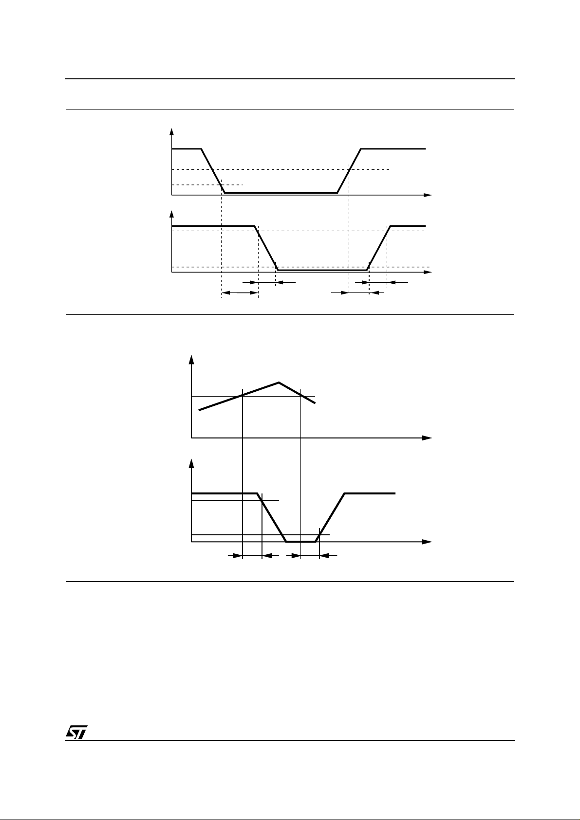
Figure 1. Switching Characteristic Definition
EN
V
th(ON)
V
th(OFF)
I
OUT
90%
10%
D01IN1316
t
D(OFF)EN
Figure 2. Ove rcurrent Detect i on Timi ng Definition
I
OUT
t
FALL
t
D(ON)EN
t
RISE
L6206
t
t
OCD
Threshold
V
OCD
90%
10%
t
OCD(ON)
t
OCD(OFF)
D01IN1222
t
t
7/23

L6206
5
6
CIRCUIT DESCRIPTION
POWER STAGES and CHARGE PUMP
The L6206 integrates two independent Power MOS
Full Bridges. Each Power MOS has an Rdson=0.3ohm (typical value @ 25°C), with intrinsic
fast freewheeling diode. Cross conduction protection
is achieved using a dead time (td = 1
µ
s typical) between the switch off and swi tch on of two P ower MOS
in one leg of a bridge.
Using N Channel Power MOS for the upper transistors in the bridge requires a gate drive voltage above
the power supply voltage. The Bootstrapped (Vboot)
supply is obtained through an internal Oscillator and
few external components to realize a charge pump
circuit as shown in Figure 3. The oscillator output
(VCP) is a square wave at 600kHz (typical) with 10V
amplitude. Recommended values/part numbers for
the charge pump circuit are shown in Table1.
Table 1. Charge Pump External Components
Values
C
BOOT
C
P
R
P
D1 1N4148
D2 1N4148
220nF
10nF
100Ω
Figure 3. Char ge Pump Circu it
V
S
D2
C
BOOT
VS
B
D01IN1328
A
D1
R
P
C
P
VCP VBOOT VS
these pins. Two configurations are shown in Fig. 5
and Fig. 6. If driven by an open drain (collec tor) structure, a pull-up resistor R
and a capacitor CEN are
EN
connected as shown in Fig. 5. If the driver is a standard Push-Pull structure the resis tor R
pacitor C
resistor R
Ω
2.2k
C
are respectively 100KΩ and 5.6nF. More infor-
EN
are connected as shown in Fig. 6. The
EN
should be chosen in the range from
EN
to 180KΩ. Recommended values for REN and
and the ca-
EN
mation on selecting the values is found in the Overcurrent Protection section.
Figure 4. Logi c Inp ut s I nte rn a l St ructure
5V
ESD
PROTECTION
D01IN1329
Figure 5. EN
and ENB Pins Open Collector
A
Driving
OPEN
COLLECTOR
OUTPUT
Figure 6. EN
PUSH-PULL
OUTPUT
OCDA or OCD
5V
R
EN
C
EN
and ENB Pins Push-Pull Driving
A
OCDA or OCD
R
EN
C
EN
ENA or EN
ENA or EN
B
5V
B
D02IN135
B
5V
B
D02IN135
LOGIC INPUTS
Pins IN1A, IN2A, IN1B, IN2B, ENA and ENB are TTL/
CMOS and uC compatible logic inputs. The internal
structure is shown in Fig. 4. Typical value for turn-on
and turn-off thresholds are respectively Vthon=1.8V
and Vthoff = 1.3V.
Pins EN
and ENB are commonly used to implement
A
Overcurrent and Thermal protection by connecting
them respectively to the outputs OCD
and OCDB,
A
which are open-drain outputs. If that type of connection is chosen, some care needs to be taken in driving
8/23
TRUTH TABLE
INPUTS OUTPUTS
EN IN1 IN2 OUT1 OUT2
L X X High Z High Z
H L L GND GND
H H L Vs GND
HLHGNDVs
HHHVsVs
X = Don't care
High Z = High Impedance Output

L6206
NON-DISSIPATIVE OVERCURRENT DETECTION AND PROTECTION
In addition to the PWM current control, an overcurrent detection circuit (OCD) is integrated. This circuit can be
used to provides protection against a short circuit to ground or between two phases of the bridge as well as a
roughly regulation of the load c urrent. With this internal over current detecti on, the exter nal current sense r esistor normally used and its associated power dissipation are eliminated. Fig. 7 shows a simplified schematic of
the overcurrent detection circuit for the Bridge A. Bridge B is provided of an analogous circuit.
To implement the over current detection, a sensing element that deli ver s a small but precise fraction of the output current is implemented with each high side power MOS. Since this current is a small fraction of the output
current there is very little additional power dissipation. This current is compared with an internal reference current I
condition. When a fault condition is detected, an internal open drain MOS with a pull down capability of 4mA
connected to OCD pin is turned on. Fig. 8 shows the OCD operation.
This signal can be used to regulate the output current simply by connecting the OCD pin to EN pin and adding
an external R-C as shown in Fig.7. The off time before recovering normal operation can be easily programmed
by means of the accurate thresholds of the logic inputs.
I
REF
. When the output current reaches the detection threshold Isover the OCD comparator signals a fault
REF
and, therefore, the output curren t detection threshold ar e selectabl e by RCL value, following the equati ons:
– Isover = 5.6A ±30% at -25°C < T
22100
– Isover = ±10% at -25°C < T
----------------
R
CL
< 125°C if RCL = 0Ω (PROGCL connected to GND)
j
< 125°C if 5K
j
Ω <
RCL < 40k
Ω
Fig. 9 shows the output current protection threshold versus RCL value in the range 5kΩ to 40kΩ.
The Disable Ti m e t
DISABLE
rate thresholds of the logic inputs. It is affected whether by C
Figure 10. The Delay Time t
only by C
C
is also used for providing immunity to pin EN against fast transient noises. Therefore the value of CEN should
EN
value. Its magnitude is re ported in Fi gure 11.
EN
be chosen as big as possible according to the maximum tolerable Delay Time and the R
before recovering normal operation can be easily programmed by means of the accu-
and REN values and its magnitude is reported in
before turning off the bridge when an overcurrent has been detected depends
DELAY
EN
value should b e chosen
EN
accord ing to the desired Disable Time.
The resistor R
should be chosen in the range from 2.2KΩ to 180KΩ. Recom men de d va lu es fo r REN and C
EN
are respe c tiv el y 10 0KΩ and 5.6nF that allow obtaining 200µs Disable Time.
EN
9/23

L6206
Figure 7. Overcurrent Protection Simplified Schematic
POWER SENSE
1 cell
µC or LOGIC
TO GATE
LOGIC
+5V
R
ENA
C
ENA
EN
OCD
A
A
R
DS(ON)
40Ω TYP.
INTERNAL
OPEN-DRAIN
Figure 8. Overcurrent Protection Wavefor ms
POWER DMOS
n cells
OCD
COMPARATOR
OVER
TEMPERATURE
PROGCL
OUT1
I
1A
A,
A
I
1A I2A
/ n
R
OUT2
VS
A
+
(I1A+I2A) / n
I
REF
I
REF
.
CLA
A
POWER DMOS
n cells
I
/ n
2A
-
1.2V
+
HIGH SIDE DMOSs OF
THE BRIDGE A
POWER SENSE
1 cell
D02IN1354
I
OUT
I
SOVER
V
EN
V
V
th(ON)
V
th(OFF)
ON
OCD
OFF
ON
BRIDGE
OFF
DD
t
OCD(ON)
t
DELAY
t
EN(FALL)
t
D(OFF)EN
t
OCD(OFF)
V
EN(LOW)
t
DISABLE
t
EN(RISE)
t
D(ON)EN
D02IN1400
10/23
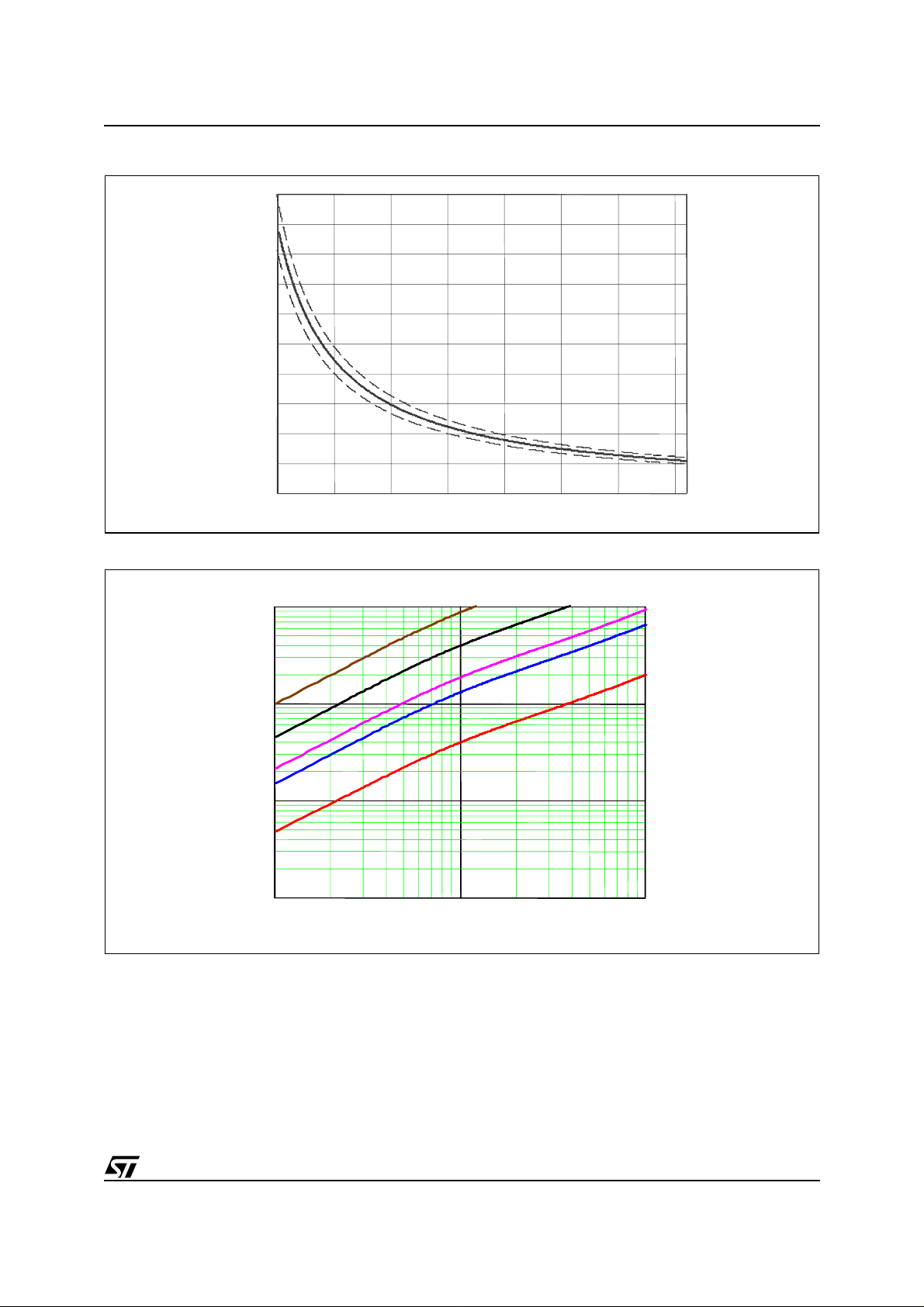
Figure 9. Out put C ur re nt P rot ec ti on Threshold ve rsus RCL Value
L6206
Figure 10. t
I
SOVER
[A]
DISABLE
1.10
1.10
5
4.5
4
3.5
3
2.5
2
1.5
1
0.5
0
5k 10k 15k 20k 25k 30k 35k 40k
versus CEN and R
3
3
EN (VDD
REN= 220 k
REN= 220 k
= 5V).
[
R
Ω
CL
Ω
Ω
]
REN= 100 k
REN= 100 k
Ω
Ω
R
R
R
R
EN
EN
EN
EN
= 47 k
= 47 k
= 33 k
= 33 k
Ω
Ω
Ω
Ω
Ω
R
R
= 10 k
= 10 k
EN
EN
100
100
[µs]
[µs]
DISABLE
DISABLE
t
t
10
10
1
1
1 10 100
1 10 100
CEN[nF ]
CEN[nF]
Ω
11/23

L6206
Figure 11. t
DELAY
versus C
10
s]
µ
tdelay [
0.1
EN (VDD
1
1 10 100
= 5V).
Cen [nF]
THERMAL PROTECTION
In addition to the Ovecurrent Detection, the L6206 integrates a Thermal Protection for preventing the device
destruction in case of junction over temperature. It works sensing the die temperature by means of a sensible
element integrated in the die. The device switch-off when the junction temperature reaches 165°C (typ. value)
with 15°C hysteresis (typ. value).
12/23

L6206
APPLICATION INFORMATION
A typical application using L6206 is shown in Fig. 12. Typical component values for the application are shown
in Table 2. A high quality ceramic capacitor in the range of 100 to 200 nF should be placed between the power
pins (VS
reduce high frequency transients generated by the switching. The capacitors connected from the EN
and ENB/OCDB nodes to ground set the shut down time for the Brgidge A and Bridge B respectively when an
over current is detected (see Overcurrent Protection). The two current sources (SENSE
be connected to Power Ground with a trace length as short as possible in the layout. To increase noise immunity, unused logic pins are best connected to 5V (High Logi c Level) or GN D (Low Logic Level) ( see pin des cription). It is recommended to keep Power Ground and Signal Ground separated on PCB.
Table 2. Component Values for Typical Application
C
C
C
C
C
C
C
and VSB) and ground near the L6206 to improve the high frequenc y fil t ering on the power supply and
A
and SENSEB) should
A
1
2
BOOT
P
ENA
ENB
REF
100uF D
100nF D
220nF R
10nF R
5.6nF R
5.6nF R
68nF R
1
2
CLA
CLB
ENA
ENB
P
1N4148
1N4148
5KΩ
5KΩ
100kΩ
100kΩ
100Ω
/OCD
A
A
Figure 12. Typical Application
+
VS
8-52V
DC
POWER
GROUND
-
SIGNAL
GROUND
C
1
C
2
C
BOOT
D
1
LOAD
LOAD
VS
A
20
B
17
R
P
VCP
22
C
D
P
2
VBOOT
SENSE
SENSE
OUT1
A
OUT2
B
OUT1
OUT2
GND
GND
GND
GND
15
A
3
B
10
A
5
A
21
B
8
B
16
18
19
6
7
4VS
23
9
14
11
12
1
2
24
13
D02IN1344
OCD
A
EN
A
OCD
B
EN
B
IN1
B
IN2
B
IN1
A
IN2
A
PROGCL
PROGCL
R
ENA
C
ENA
R
ENB
C
ENB
A
R
CLA
B
R
CLB
IN1
IN2
IN1
IN2
EN
A
EN
B
B
B
A
A
13/23
L6206
PARALLELED OPERATION
The outputs of the L6206 can be paralleled to increase the output current capability or reduce the power dissipation in the device at a given current level. It must be noted, however, that the internal wire bond connections
from the die to the power o r sense pins of the package m ust ca rry cur rent in both of the as sociated half bridges.
When the two halves of one full bridge (for example OUT1
current rating is not increased since the total current must still flow through one bond wire on the power supply
or sense pin. In addition the over current detection senses the sum of the current in the upper devices of each
bridge (A or B) so connecting the two halves of one bridge in parallel does not increase the over current detection threshold.
For most applications the recommended configuration is Half Bridge 1 of Bridge A paralleled with the Half Bridge
1 of the Bridge B, and the same for the Half Bridges 2 as shown in Figure 13. The current in the two devices
connected in parallel will share very well since the R
DS(ON)
When connected in this configuration the over cur rent detection circuit, whic h sens es the c urrent in each br idge
(A and B), will sense the c urrent in upper devices connected in par allel independentl y and the sens e circ uit with
the lowest threshold will trip first. With the enables connected in parallel , the first detection of an over current in
either upper DMOS device will turn of both bridges. Assuming that the two DMOS devices share the current
equally, the resulting over current detection threshold will be twice the minimum threshold set by the resistors
R
CLA
or R
in figure 13. It is recommended to use R
CLB
In this configuration the resulting Bridge has the following characteristics.
- Equivalent Device: FULL BRIDGE
- R
0.15Ω Typ. Value @ TJ = 25°C
DS(ON)
- 5.6A max RMS Load Current
- 11.2A max OCD Threshold
and OUT2A) are connected in parallel, the peak
A
of the devices on the same die is well matched.
CLA
= R
CLB
.
Figure 13. Parallel connection for higher current
VS
VS
8-52V
+
DC
POWER
GROUND
-
SIGNAL
GROUND
LOAD
C
1
C
2
D
1
R
P
BOOT
D
2
C
VS
VCP
C
P
VBOOT
SENSE
SENSE
OUT1
OUT2
OUT1
OUT2
GND
GND
GND
GND
A
B
A
B
A
A
B
B
20
17
22
15
3
10
5
21
8
16
18
19
6
7
9
14
4
1
2
11
12
24
13
D02IN1364
OCD
B
EN
B
OCD
A
EN
A
IN1
A
IN2
A
IN1
B
IN2
B
PROGCL
PROGCL
R
EN
C
EN
A
R
CLA
B
R
CLB
EN23
IN1
IN2
14/23
L6206
To operate the device in parallel and maintain a lower over current threshold, Half Bridge 1 and the Half Bridge
2 of the Bridge A can be connected in parallel and the same done for the B ridge B as shown in Figure 14. In
this configuration, the pe ak c urrent for eac h hal f bridge is stil l l imited by the bond wi res for the s upply and s ense
pins so the dissipation in the device will be reduced, but the peak current rating is not increased.
When connected in this configuration the over current detection circuit, senses the sum of the current in upper
devices connected in parallel. With the enables connected in parallel, an over current will turn of both bridges.
Since the circui t senses the total curr ent in th e upper devices , the over current threshol d is equal to the thr eshold
set the resistor R
and resistor R
It is recommended to use R
In this configuration, the resulting bridge has the following characteristics.
- Equivalent Device: FULL BRIDGE
- R
0.15Ω Typ. Value @ TJ = 25°C
DS(ON)
- 2.8A max RMS Load Current
- 5.6A max OCD Threshold
Figure 14. Parallel connection with lower Over current Threshold
+
VS
8-52V
DC
POWER
GROUND
-
SIGNAL
GROUND
LOAD
C
or R
CLA
sets the threshold when outputs OUT1B and OUT2B are high.
CLB
1
in figure 14. R
CLB
= R
CLA
C
2
D
1
C
BOOT
CLB
sets the threshold when outputs OUT1A and OUT2A are high
CLA
.
VS
A
20
VS
B
17
R
VCP
P
C
D
P
2
VBOOT
SENSE
SENSE
OUT1
OUT2
OUT1
OUT2
GND
GND
GND
GND
22
15
A
3
B
10
A
5
A
21
B
8
B
16
18
19
6
7
4
23
9
14
1
2
11
12
24
13
D02IN1361
OCD
A
EN
A
OCD
B
EN
B
IN1
A
IN2
A
IN1
B
IN2
B
PROGCL
PROGCL
R
EN
C
EN
A
R
CLA
B
R
CLB
EN
IN
A
IN
B
15/23
L6206
It is also possible to parallel the four Half B ridges to obtain a simple Half Bridge as shown in Fig. 15. In this
configuration the, the over current threshold is equal to twice the minimum threshold set by the resistors R
or R
in Figure 15. It is recommended to use R
CLB
CLA
= R
CLB
.
The resulting half bridge has the following characteristics.
- Equivalent Device: HALF BRIDGE
- R
0.075Ω Typ. Value @ TJ = 25°C
DS(ON)
- 5.6A max RMS Load Current
- 11.2A max OCD Threshold
Figure 15. Paralleling the four Half Bridges
VS
A
VCP
GND
GND
GND
GND
20
B
17
22
15
A
3
B
10
A
5
A
21
B
8
B
16
18
19
6
7
23
14
11
12
24
13
4VS
9
1
2
OCD
A
EN
A
OCD
B
EN
B
IN1
A
IN2
A
IN1
B
IN2
B
PROGCL
PROGCL
D02IN1365
R
EN
C
EN
A
R
CLA
B
R
CLB
VS
8-52V
+
DC
POWER
GROUND
-
SIGNAL
GROUND
C
1
C
2
D
1
R
P
C
C
BOOT
D
P
2
VBOOT
SENSE
SENSE
OUT1
OUT2
LOAD
OUT1
OUT2
CLA
EN
IN
16/23

L6206
OUTPUT CURRENT CAPABILITY AND IC POWER DISSIPATION
In Fig. 16 and Fig. 17 are show n the approxi mate relation between the output current and the IC power dis sipation using PWM current control driving two loads, for two different driving types:
– One Full Bridge ON at a time (Fig.16) in which only one load at a time is energized.
– Two Full Bridges ON at the same time (Fig.17) in which two loads at the same time are energized.
For a given output current and driving type the power dissipated by the IC can be easily evaluated, in order to
establish which package should be used and how large must be the on-board copper dissipating area to guarantee a safe operating junction temperature (125°C maximum).
Figure 16. IC Power Dissipation versus Output Curr ent with One Full Bridge ON at a time.
ONE FULL BRIDGE ON AT A TIME
10
I
A
I
OUT
8
6
PD [W]
4
I
B
I
OUT
Test Conditions:
2
Supply Voltage = 24V
No PWM
0
0 0.5 1 1.5 2 2.5 3
I
[A]
OUT
f
= 30kHz (slow decay)
SW
Figure 17. IC Power Dissipation versus Output Current with Two Full Bridges ON at the same time.
TWO FULL BRIDGES ON AT THE SAME TIME
10
8
6
PD [W]
4
2
0
00.511.522.53
I
[A]
OUT
I
A
I
B
I
OUT
I
OUT
Test Conditions:
Supply Voltage = 24V
No PWM
= 30kHz (slow decay)
f
SW
THERMAL MANAGEMENT
In most applic ations the power dissipation in the IC is the main factor that sets th e max imum current that can be deliver by the device in a safe operating con dit i on. Therefore, i t ha s to be taken into account very car efully. Besides the
available space on the PCB, the r igh t package should be chosen considering the p ower dissipati on. Heat sin ki ng can
be achieved using copper on the PCB with proper area and thickness. Figures 19, 20 and 21 show the Junction-toAmbient Thermal Resistance values for the PowerSO36, PowerDIP24 and SO24 packages.
For instance, using a PowerSO package with copper slug soldered on a 1.5 mm copper thickness FR4 board
with 6cm
2
dissipating footprint (cop per thicknes s of 35µm), the R
is about 35°C/W. Fig. 18 shows mount-
th j-amb
ing methods for this package. Using a multi- layer board wi th vias to a ground plane, thermal impeda nce can be
reduced down to 15°C/W.
17/23

L6206
Figure 18. Mounting the PowerSO pack age.
Slug soldered
to PCB with
dissipating area
Slug soldered
to PCB with
dissipating area
plus ground layer
Slug soldered to PCB with
dissipating area plus ground layer
contacted through via holes
Figure 19. PowerSO36 Junction -Am bient thermal resi stance versus on-bo ard co pper area.
ºC / W
43
38
33
28
23
18
13
12345678910111213
Without Ground Layer
With Ground Layer
With Ground Layer+16 via
Holes
sq. cm
On-Board Copper Area
Figure 20. PowerDIP24 Junction-Ambient thermal resistance versus on-board copper area.
ºC / W
49
48
47
46
45
44
43
42
41
40
39
1 2 3 4 5 6 7 8 9 101112
Copper Area is on Bottom
Side
Copper Area is on Top Side
sq . cm
On-Board Copper Area
Figure 21. SO24 Junction-Ambient thermal resi stance versus on-bo ard copp er area.
18/23
ºC / W
68
66
64
62
60
58
56
54
52
50
48
123456789101112
Copper Area is on Top Side
sq. cm
On-Board Copper Area

L6206
Figure 22. Typical Quiescent Current vs.
Supply Voltage
Iq [mA ]
5.6
5.4
fsw = 1kHz Tj = 25°C
Tj = 85°C
Tj = 125°C
5.2
5.0
4.8
4.6
0 102030405060
[V]
V
S
Figure 23. Normalized Typical Quiescen t
Current vs. Switching Frequency
Iq / (Iq @ 1 kHz)
1.7
1.6
1.5
1.4
1.3
1.2
1.1
1.0
0.9
0 20406080100
[kHz]
f
SW
Figure 25. Typical High-Side RDS (ON) vs.
Supply Voltage
R
[Ω]
DS(ON)
0.380
0.376
0.372
0.368
0.364
0.360
0.356
0.352
0.348
0.344
0.340
0.336
0 5 10 15 20 25 30
Figure 26. Normalized R
Tj = 25°C
[V]
V
S
DS(ON)
vs.Junction
Temperature (typical value)
/ (R
R
DS(ON)
1.8
1.6
1.4
1.2
1.0
0.8
0 20406080100120140
DS(ON)
@ 25 °C)
Tj [°C]
Figure 24. Ty pi cal Lo w- S i de R
DS(ON)
Supply Voltage
[Ω]
R
DS(ON)
0.300
0.296
Tj = 25°C
0.292
0.288
0.284
0.280
0.276
0 5 10 15 20 25 30
V
[V]
S
vs.
Figure 27. Typical Drain-Source Diode
Forward ON Characteristic
I
[A]
SD
3.0
2.5
2.0
1.5
1.0
0.5
0.0
700 800 900 1000 1100 1200 1300
Tj = 25°C
V
[mV]
SD
19/23

L6206
DIM.
MIN. TYP. MAX. MIN. TYP. MAX.
mm inch
A 3.60 0.141
a1 0.10 0.30 0.004 0.012
a2 3.30 0.130
a3 0 0.10 0 0.004
b 0.22 0.38 0.008 0.015
c 0.23 0.32 0.009 0.012
D (1) 15.80 16.00 0.622 0.630
D1 9.40 9.80 0.370 0.385
E 13.90 14.50 0.547 0.570
e 0.65 0.0256
e3 11.05 0.435
E1 (1) 10.90 11.10 0.429 0.437
E2 2.90 0.114
E3 5.80 6.20 0.228 0.244
E4 2.90 3.20 0.114 0.126
G 0 0.10 0 0 .004
H 15.50 15.90 0.610 0.626
h 1.10 0.043
L 0.80 1.10 0.031 0.043
N10°(max.)
S8°(max.)
(1): "D" and "E1" do not include mold flash or protrusions
- Mold flash or protrusions shall not exceed 0.15mm (0.006 inch)
- Critical dimensions are "a3", "E" and "G".
OUTLINE AND
MECHANICAL DATA
PowerSO36
E2
h x 45˚
NN
a2
A
1936
0.12 AB
⊕
e
a3
B
E1
Gage Plane
M
PSO36MEC
DETAIL A
118
A
e3
H
D
b
DETAIL B
lead
BOTTOM VIEW
DETAIL B
0.35
S
DETAIL A
L
a1
E
slug
D1
SEATING PLANE
(COPLANARITY)
c
- C -
GC
E3
20/23
L6206
DIM.
MIN. TYP. MAX. MIN. TYP. MAX.
A 4.320 0.170
A1 0.380 0.015
A2 3.300 0.130
B 0.410 0.460 0.510 0.016 0.018 0.020
B1 1.400 1.520 1.650 0.055 0.060 0.065
c 0.200 0.250 0.300 0.008 0.010 0.012
D 31.62 31.75 31.88 1.245 1.250 1.255
E 7.620 8.260 0.300 0.325
e 2.54 0.100
E1 6.350 6.600 6.860 0.250 0.260 0.270
e1 7.620
L 3.180 3.430 0.125 0.135
M 0˚ min, 15˚ max.
mm inch
0.300
OUTLINE AND
MECHANICAL DATA
Powerdip 24
E1
A2
A
13
12
A1
SDIP24L
e1
c
M
L
B eB1
D
24
1
21/23

L6206
DIM.
MIN. TYP. MAX. MIN. TYP. MAX.
A 2.35 2.65 0.093 0.104
A1 0 .10 0.30 0.004 0.012
B 0.33 0.51 0.013 0.200
C 0.23 0.32 0.009 0.013
(1)
15.20 15.60 0.598 0.614
D
E 7.40 7.60 0.291 0.299
e 1.2 7 0.050
H 10.0 10.65 0.394 0.419
h 0.25 0;75 0.010 0.030
L 0.40 1.27 0.016 0.050
k 0˚ (min.), 8˚ (max.)
ddd 0.10 0.004
(1) “ D” dimension does not includ e mold flas h, prot u s ions or gate
burrs. Mo ld f las h, p rotus ion s or g at e bur rs sh all not exce ed
0.15mm per side.
mm inch
OUTLINE AND
MECH AN ICAL DAT A
Weight: 0.60gr
SO24
22/23
0070769 C

L6206
Information furnished is believed to be accurate and reliable. However, STMicroelectronics assumes no responsibility for the consequences
of use of such information nor for any infringement of patents or other rights of third parties which may result from its use. No license is granted
by implic ation or o therwise under any patent or p atent right s of STMicroelectronics. Specificat ions ment i oned in th i s publicati on are subj ect
to change without notice. This publication supersedes and replaces all information previously supplied. STMicroelectronics product s are not
authoriz ed for use as critical comp onents in life support devices or systems without express wri tten appr oval of STMicroelectronics.
The ST logo is a registered trademark of STMicroelectr oni cs.
All other names are the propert y of their respective owners
© 2003 STMi croelectro nics - All right s reserve d
Australi a - Belgium - Brazil - Canada - China - C zech Republi c - Finlan d - F rance - Germany - Hong Kon g - India - Israel - Italy - Japan -
Malaysia - Malta - Morocco - Singapore - Spain - Sweden - Switzerland - United Kingdom - United States
STMicroelectronics GROUP OF COMPANIES
www.st.com
23/23
 Loading...