

L6204
DMOS DUAL FULL BRIDGE DRIVER
ADVANCE DATA
SUPPLYVOLTAGEUP TO 48V
DS(ON)
1.2Ω (25°C)
R
CROSS CONDUCTION PROTECTION
THERMAL SHUTDOWN
0.5A DC CURRENT
TTL/CMOSCOMPATIBLEDRIVER
HIGHEFFICIENCYCHOPPING
DESCRIPTION
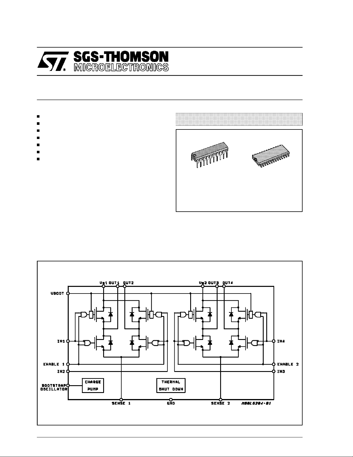
The L6204 is a dual full bridge driver for motor
control applications realized in BCD technology
which combines isolated DMOS power transistors
with CMOS and Bipolar circuitson the same chip.
By using mixed technologyit has been possible to
optimizethe logic circuitry and the power stage to
achievethe best possibleperformance.
The logic inputs are TTL/CMOS compatible. Both
channelsare controlled by a separate Enable.
Each bridge has a sense resistor to control the
currenrt level.
BLOCK DIAGRAM
MULTIPOWERBCD TECHNOLOGY
Powerdip 16+2+2 SO 24+2+2
ORDERING NUMBERS:
L6204 L6204D
The L6204 is mounted in an 20-lead Powerdip
and SO 24+2+2 packages and the four center
pins are used to conduct heat to the PCB. At normal operating temperatures no external heatsink
isrequired.
March 1994
This isadvanced information on a new product now in development or undergoing evaluation. Details are subject to change without notice.
1/10

L6204
PIN CONNECTIONS (Topview)
POWERDIP
PIN FUNCTIONS
SO
DIP
Pin
Pin
(*)
1
1
2
2
3
3
4
6
5
7
6
8
7
9
8
12
9
13
10
14
11
15
12
16
13
17
14
20
15
21
16
22
17
23
18
26
19
27
20
28
(*) For SOpackage the pins 4, 5, 10, 11, 18, 19, 24 and 25 arenot connected.
ABSOLUTE MAXIMUM RATINGS
Symbols Functions
SENSE 1
IN1
ENABLE 1
OUT 1
GND
GND
OUT 3
ENABLE 2
IN 3
SENSE 2
BOOSTRAP OSC. VCP
IN 4
OUT 4
V
2
S
GND
GND
V
1
S
OUT 2
IN 2
VBOOT
Sense resistorto providethe feedback for motor current control of the bridge A
Digital input from the motor controller (bridge A)
A logic level low on this pin disable the bridge A
Output ofone half bridge of the bridge A
Common Power Ground
Common Power Ground
Ouput of one half bridge of the bridge B
A logic level low on this pin disable the bridge B
Digital input from the motor controller (bridge B)
Sense resistorto providethe feedback for motor current control of the bridge B
Oscillator output for the external charge pump
Digital input from the motor controller (bridge B)
Output ofone half bridge of the bridge B
Supply voltage bridge B
Common Power Ground
Common Power Ground
Supply Voltage bridge A
Output ofone half bridge of the bridge A
Digital input from the motor controller (bridge A)
Overvoltage input for driving of the upper DMOS
SO24+2+2
Symbol Parameter Test Conditions Unit
V
V
IN,VEN
V
SENSE
V
BOOT
P
T
stg,Tj
Supply Voltage 50 V
S
Input or Enable Voltage Range -0.3 to +7 V
Pulsed Output Current 3 A
I
o
Sensing Voltage -1 to 4 V
Bootstrap Supply 60 V
Total power dissipation: (T
tot
Total power dissipation: (T
Total power dissipation: (T
=80°C)
pins
=70°C no copper area on PCB)
amb
=70°C 8cm2copperarea on PCB)
amb
5
1.23
2
Storage and Junction Temperature -40 to 150 °C
2/10
W
W
W
THERMAL DATA
Symbol Description SO DIP Unit
R
th j-pins
R
th j-amb
Thermal Resistance Junction-pins
Thermal Resistance Junction-ambient
Max
Max
16
73
14
65
ELECTRICALCHARACTERISTICS (VS= 42V, Tj=25°C unless otherwisespecified)
Symbol Parameter Test Condition Min. Typ. Max. Unit
V
I
f
T
T
Supply Voltage 12 48 V
S
Total Quiescent Current EN1=EN2=H;IN1=IN2=IN3=IN4=L
S
EN1 = EN2 = L
Commutation Frequency 20 KHz
C
Thermal Shutdown 150 °C
J
Dead Time Protection 500 ns
d
10
10
TRANSISTORS
L6204
°C/W
°C/W
mA
mA
I
R
DSS
Leakage Current OFF 1 mA
On Resistance ON 1.2 Ω
DS
LOGICLEVELS
V
INL,VENL
V
INH,VENH
I
INL,IENL
I
INH,IENH
Input Low Voltage -0.3 0.8 V
Input High Voltage 2 7 V
Input Low Current IN1=IN2=IN3=IN4=EN1 =EN2=L -10 µA
Input High Current IN1=IN2 =IN3=IN4=EN1=EN2=H 50 µA
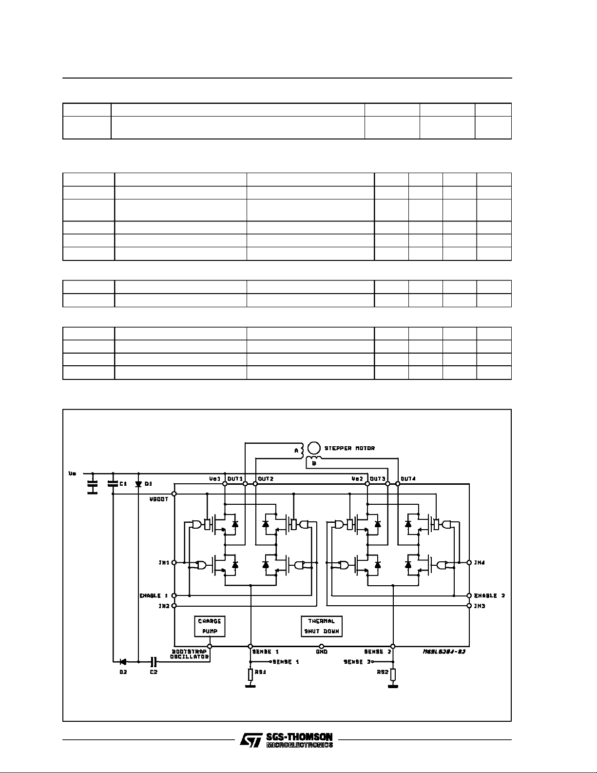
APPLICATION DIAGRAM
3/10

L6204
CIRCUITDESCRIPTION
L6204 is a dual full bridge IC designed to drive
DC motors, stepper motors and other inductive
loads. Each bridge has 4 power DMOS transistor
with R
= 1.2Ω and the relative protection and
DSon
controlcircuitry. (see fig. 3)
The4 half bridges can be controlled independently
by means of the 4 inputsIN!, IN2, IN3, IN4 and 2
enableinputsENABLE1 andENABLE2.
Externalconnections are provided so that sensing
resistors can be added for constant current chopperapplications.
LOGICDRIVE (*)
INPUTS
IN1
IN3
EN1=EN2=H
EN1=EN2=L X X All transistor turned
L =Low H = High X =Don’t care
(*) True table for the two full bridges
L
L
H
H
OUTPUT MOSFETS
IN2
IN4
Sink 1, Sink 2
L
Sink 1, Source 2
H
Source 1, Sink 2
L
Source 1, Source 2
H
OFF
CROSSCONDUCTION
Although the device guarantees the absence of
cross-conduction,the presence of the intrinsic diodes in the POWER DMOS structure causes the
generationof current spikes on the sensing terminals. This is due to charge-dischargephenomena
in the capacitors C1 & C2 associated with the
drain source junctions (fig. 1). When the output
switches from high to low, a current spike is generated associated with the capacitor C1. On the
low-to-hightransition a spike of the same polarity
is generated by C2, preceded by a spike of the
opposite polarity due to the charging of the input
capacity of the lower POWER DMOS transistor
(see fig. 2).
Figure1: IntrinsicStructures in the POWER
MOS Transistors
Figure 2:Current Typical SpikesontheSensing Pin
TRANSISTOR OPERATION
ON STATE
Whenone of the POWERDMOS transistorsis ON
it can be consideredas a resistor R
DS(ON)
=1.2Ω at
ajunctiontemperatureof25°C.
Inthiscondition thedissipated poweris given by :
2
⋅ I
DS
The low R
P
DS(ON)
ON=RDS(ON)
of the Multipower-BCD process
can provide high currents with low power dissipation.
OFFSTATE
When one of the POWER DMOS transistor is
OFF the V
age and only the leakage current I
voltage is equal to the supply volt-
DS
flows. The
DSS
powerdissipation during this period is given by :
P
OFF=VS⋅IDSS
TRANSITIONS
Like all MOS power transistors the DMOS
POWER transistors have as intrinsic diode between their source and drain that can operate as
a fast freewheelingdiode in switched mode applications. During recirculation with the ENABLE input high, the voltage drop across the transistor is
R
DS(ON)
.
IDand when the voltage reaches the diode voltage it is clamped to its characteristic.
When the ENABLE input is low, the POWER
MOS is OFF and the diode carries all of the recirculationcurrent. The powerdissipated in the transitional times in the cycle depends upon the voltage and currentwaveforms in the application.
P
trans.=IDS
(t)⋅ VDS(t)
4/10
BOOTSTRAP CAPACITORS
To ensure the correct driving of high side drivers

Figure3a: Two Phase Chopping
L6204
IN1 = H
IN2 = L
EN1 = H
Figure3b: One PhaseChopping
IN1 = H
IN2 = L
EN1 = H
IN1 = L
IN2 = H
EN1 = H
IN1 = H
IN2 = H
EN1 = H
Figure3c: EnableChopping
IN1 = H
IN2 = L
EN1 = H
IN1 = X
IN2 = X
EN1 = L
5/10

L6204
a voltage higher than VSis supplied on pin 20
). This bootstrap voltage is not needed for
(V
boot
the lower power DMOS transistor because their
sources are grounded. To produce this voltage a
charge pump method is used and mAde by two
external capacitors and two diodes. It can supply
the 4 driving blocksof the high side drivers. Using
an external capacitor the turn-on speed of the
high side driver is very high; furthermore with different capacitance values it is possible to adapt
the device to different switching frequencies. It is
also possible to operate two or more L6204s using only 2 diodes and 2 capacitance for all the
ICs; all the Vboot pins are connected to the C
store
capacitance while the pin 11 (VCP) of just one
L6204 is connect to C
L6204 ICs have to be connected to the same V
, obviously all the
pump
S
(see fig. 4)
Figure4
the voltage created across the sense resistor is
usuallymuch less thanthe peak value, although a
smallRC filtercan be added if necessary.
POWERDISSIPATION(each bridge)
In order to achieve the high performance provided
by the L6204 some attention must be paid to ensure that it has an adequate PCB area to dissipate the heat. The first stage of any thermal design is to calculate the dissipated power in the
application, for this example the half step operationshown in figure 5 is considered.
RISE TIMET
When an arm of the half bridge is turned on cur-
.
rent begins to flow in the inductive load until the
maximum current I
Thedissipated energy E
E
OFF/ON
r
is reached after a time Tr.
L
isin this case :
2
⋅ I
⋅ Tr] ⋅ 2/3
L
=[R
OFF/ON
DS(ON)
Figure5
DEAD TIME
To protect the device against simultaneous con-
duction in both arms of the bridge and the resulting rail-to-rail short, the logic circuits provide a
dead time.
THERMAL PROTECTION
A thermal protection circuit has been included
that will disable the device if the junction temperature reaches 150 °C. When the temperature has
fallen to a safe level the device restarts under the
controlof theinput and enable signals.
APPLICATION INFORMATION
RECIRCULATION
During recirculation with the ENABLE input high,
the voltage drop across the transistor is R
I
for voltagesless than 0.7 V and is clamped at a
L
DS(ON)
voltage depending on the characteristics of the
source-drain diode for greater voltages. Although
the device is protected against cross conduction,
current spikes can appear on the current sense
pin due to charge/dischargephenomena in the intrinsic source drain capacitances. In the application this does not cause any problems because
ON TIME T
ON
During this time the energy dissipated is due to
the ON resistance of the transistors E
commutationE
transistorsare ON E
E
. As two of the POWER DMOS
COM
ON=IL
isgiven by :
ON
2
⋅R
DS(ON)
⋅ 2 ⋅ T
ON
In the commutation the energy dissipatedis :
E
COM=VS
⋅IL ⋅ T
COM
⋅ f
SWITCH
Where:
T
= CommutationTime and itis assumedthat;
COM
T
COM=TTURN-ON=TTURN-OFF
f
.
FALL TIME T
SWITCH
= Chopperfrequency
f
=100 ns
For this example it is assumed that the energy
dissipatedin this part of the cycle takes the same
formas that shown for the risetime :
E
ON/OFF
=[R
DS(ON)
2
⋅ I
⋅ Tf] ⋅ 2/3
L
ON
⋅ T
and the
ON
6/10

L6204
QUIESCENTENERGY
The last contribution to the energy dissipation is
due to the quiescent supply current and is given
by :
E
QUIESCENT=IQUIESCENT•VS
•T
TOTALENERGYPER CYCLE
E
=(E
TOT
OFF/ON+EON+ECOM+EON/OFF)bridge 1
+(E
OFF/ON+EON+ECOM+EON/OFF)bridge2
+E
QUIESCENT
+
+
TheTotal Power Dissipation P
P
DIS=ETOT
T
=Rise time
r
=ON time
T
ON
T
= Fall Time
f
T
=Dead time
d
T = Period
T=T
r+TON+Tf+Td
is simply :
DIS
/T
7/10

L6204
POWERDIP-20 PACKAGE MECHANICAL DATA
DIM.
MIN. TYP. MAX. MIN. TYP. MAX.
a1 0.51 0.020
B 0.85 1.40 0.033 0.055
b 0.50 0.020
b1 0.38 0.50 0.015 0.020
D 24.80 0.976
E 8.80 0.346
e 2.54 0.100
e3 22.86 0.900
F 7.10 0.280
I 5.10 0.201
L 3.30 0.130
Z 1.27 0.050
mm inch
8/10

SO28PACKAGE MECHANICAL DATA
L6204
DIM.
MIN. TYP. MAX. MIN. TYP. MAX.
A 2.65 0.104
a1 0.1 0.3 0.004 0.012
b 0.35 0.49 0.014 0.019
b1 0.23 0.32 0.009 0.013
C 0.5 0.020
c1 45° (typ.)
D 17.7 18.1 0.697 0.713
E 10 10.65 0.394 0.419
e 1.27 0.050
e3 16.51 0.65
F 7.4 7.6 0.291 0.299
L 0.4 1.27 0.016 0.050
S8°(max.)
mm inch
9/10

L6204
Information furnished is believed to be accurate and reliable. However, SGS-THOMSON Microelectronics assumes no responsibility for the
consequences of use of such information nor for any infringement of patents or other rights of third parties which may result from itsuse. No
license is granted by implication or otherwise under any patent or patent rights of SGS-THOMSON Microelectronics. Specifications mentioned in this publication are subject to change without notice. This publication supersedes and replaces all information previously supplied.
SGS-THOMSON Microelectronics products are not authorized for use as critical components in life support devices or systems without express written approval of SGS-THOMSON Microelectronics.
1994 SGS-THOMSON Microelectronics - All RightsReserved
Australia - Brazil - France - Germany - Hong Kong - Italy - Japan - Korea -Malaysia - Malta - Morocco - The Netherlands - Singapore -
SGS-THOMSON Microelectronics GROUPOF COMPANIES
Spain - Sweden - Switzerland - Taiwan - Thaliand- United Kingdom - U.S.A.
10/10
 Loading...