

L6201
L6202 - L6203
DMOS FULL BRIDGE DRIVER
SUPPLYVOLTAGEUP TO 48V
5AMAXPEAKCURRENT (2A max.forL6201)
TOTALRMS CURRENT UP TO
L6201: 1A;L6202:1.5A; L6203/L6201PS:4A
R
DS (ON)
0.3 Ω (typicalvalue at 25 °C)
CROSSCONDUCTION PROTECTION
TTL COMPATIBLEDRIVE
OPERATINGFREQUENCYUP TO 100 KHz
THERMALSHUTDOWN
INTERNALLOGIC SUPPLY
HIGHEFFICIENCY
DESCRIPTION
The I.C. is a full bridgedriver for motor controlapplications realized in Multipower-BCD technology
which combinesisolated DMOSpower transistors
with CMOS and Bipolar circuits on the same chip.
By using mixed technologyit has beenpossibleto
optimize the logic circuitry and thepower stage to
achieve the best possible performance. The
DMOS output transistors can operate at supply
voltages up to 42V and efficiently at high switch-
ing speeds. All the logic inputs are TTL, CMOS
andµC compatible.Each channel (half-bridge) of
the device is controlledby a separate logic input,
while a common enable controls both channels.
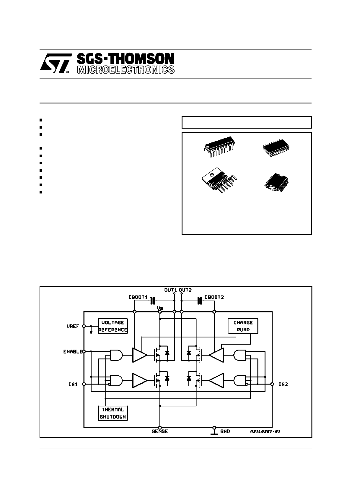
The I.C. is mountedin three different packages.
This is advanced information on a new product now in development or undergoing evaluation. Details are subjectto change without notice.
July 1997
MULTIPOWER BCD TECHNOLOGY
BLOCK DIAGRAM
ORDERING NUMBERS:
L6201 (SO20)
L6201PS
(PowerSO20)
L6202 (Powerdip18)
L6203 (Multiwatt)
SO20 (12+4+4)
Multiwatt11
Powerdip 12+3+3
PowerSO20
1/20
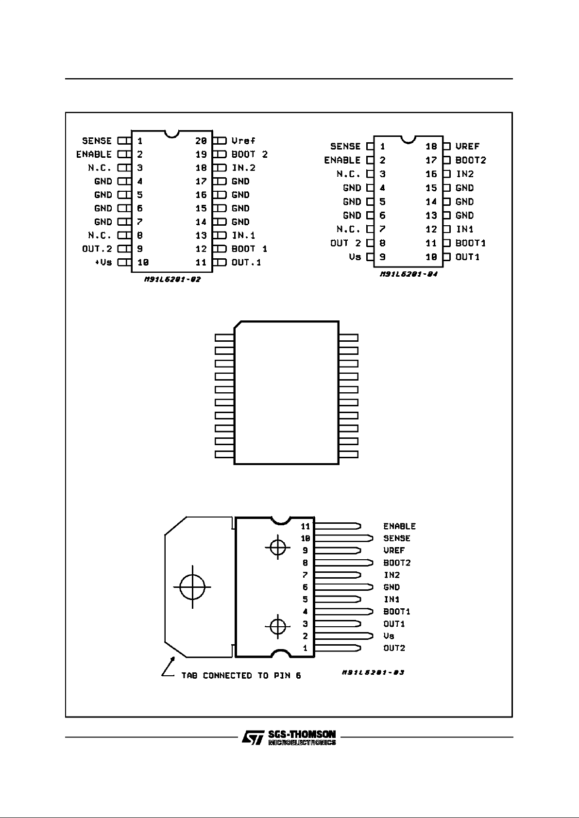
PIN CONNECTIONS (Top view)
SO20
GND
N.C.
N.C.
N.C.
OUT2
OUT1
V
S
BOOT1
IN1
N.C.
GND 10
8
9
7
6
5
4
3
2
13
14
15
16
17
19
18
20
12
1
11
GND
D95IN216
IN2
BOOT2
SENSE
Vref
ENABLE
N.C.
N.C.
GND
PowerSO20
MULTIWATT11
POWERDIP
L6201 - L6202 - L6203
2/20

PINS FUNCTIONS
Device
Name Function
L6201 L6201PS L6202 L6203
1 16 1 10 SENSE A resistor R
sense
connected to this pin provides feedback for
motor current control.
2 17 2 11 ENABLEWhen a logic high is present on this pin the DMOS POWER
transistors are enabled to be selectively driven by IN1 and IN2.
3 2,3,9,12,
18,19
3 N.C. Not Connected
4,5 – 4
6
GND Common Ground Terminal
– 1, 10 5 GND Common Ground Terminal
6,7 – 6 GND Common Ground Terminal
8 – 7 N.C. Not Connected
9481OUT2Ouput of 2nd Half Bridge
10592V
s
Supply Voltage
11 6 10 3 OUT1 Output of first Half Bridge
12 7 11 4 BOOT1 A boostrap capacitor connected to this pin ensures efficient
driving ofthe upper POWER DMOS transistor.
13 8 12 5 IN1 Digital Input from the Motor Controller
14,15 – 13
6
GND Common Ground Terminal
– 11, 20 14 GND Common Ground Terminal
16,17 – 15 GND Common Ground Terminal
18 13 16 7 IN2 Digital Input from the Motor Controller
19 14 17 8 BOOT2 A boostrap capacitor connected to this pin ensures efficient
driving ofthe upper POWER DMOS transistor.
20 15 18 9 V
ref
Internal voltage reference. A capacitor from this pin to GND is
recommended. The internal Ref. Voltage can source out a
current of 2mA max.
Symbol Parameter Value Unit
V
s
Power Supply 52 V
V
OD
Differential Output Voltage (between Out1 and Out2) 60 V
V
IN,VEN
Input or Enable Voltage – 0.3 to + 7 V
I
o
Pulsed Output Current for L6201PS/L6202/L6203 (Note 1)
– Non Repetitive (< 1 ms) for L6201
for L6201PS/L6202/L6203
DC Output Current for L6201 (Note 1)
5
5
10
1
A
A
A
A
V
sense
Sensing Voltage – 1 to + 4 V
V
b
Boostrap Peak Voltage 60 V
P
tot
Total Power Dissipation:
T
pins
=90°C for L6201
for L6202
T
case
=90°C for L6201PS/L6203
T
amb
=70°C for L6201(Note 2)
for L6202 (Note 2)
for L6201PS/L6203 (Note 2)
4
5
20
0.9
1.3
2.3
W
W
W
W
W
W
T
stg,Tj
Storage and Junction Temperature – 40 to + 150 °C
Note 1: Pulse width limitedonly by junction temperature and transient thermal impedance (see thermal characteristics)
Note 2:
Mountedon board with minimized dissipating copper area.
ABSOLUTE MAXIMUM RATINGS
L6201 - L6202 - L6203
3/20

THERMAL DATA
Symbol Parameter
Value
Unit
L6201 L6201PS L6202 L6203
Rt
h j-pins
Rt
h j-case
Rt
h j-amb
Thermal Resistance Junction-pins max
Thermal Resistance Junction Case max.
Thermal Resistance Junction-ambient max.
15
–
85
–
–
13 (*)
12
–
60
–
3
35
°C/W
(*) Mounted on aluminiumsubstrate.
ELECTRICAL CHARACTERISTICS (Refer to the Test Circuits; Tj=25°C, VS= 42V, V
sens
= 0, unless
otherwise specified).
Symbol Parameter Test Conditions Min. Typ. Max. Unit
V
s
Supply Voltage 12 36 48 V
V
ref
Reference Voltage I
REF
= 2mA 13.5 V
I
REF
Output Current 2mA
I
s
Quiescent Supply Current EN = H VIN=L
EN = H V
IN
=H
EN = L ( Fig. 1,2,3)
IL=0
10
10
8
15
15
15
mA
mA
mA
f
c
Commutation Frequency(*) 30 100 KHz
T
j
Thermal Shutdown 150
°
C
T
d
Dead Time Protection 100 ns
TRANSISTORS
OFF
I
DSS
Leakage Current Fig. 11 Vs=52V 1 mA
ON
R
DS
On Resistance Fig. 4,5 0.3 0.55 Ω
V
DS(ON)
Drain Source Voltage Fig. 9
I
DS
=1A
I
DS
= 1.2A
I
DS
=3A
L6201
L6202
L6201PS/0
3
0.3
0.36
0.9
V
V
V
V
sens
Sensing Voltage – 1 4 V
SOURCEDRAIN DIODE
V
sd
Forward ON Voltage Fig. 6a and b
I
SD
=1A
L6201
EN = L
I
SD
= 1.2A L6202 EN = L
I
SD
=3A
L6201PS/03
EN =
L
0.9 (**)
0.9 (**)
1.35(**)
V
V
V
t
rr
Reverse Recovery Time
dif
dt
=25A/µs
I
F
=1A
I
F
= 1.2A
I
F
=3A
L6201
L6202
L6203
300 ns
t
fr
Forward Recovery Time 200 ns
LOGIC LEVELS
V
IN L,VEN L
Input Low Voltage – 0.3 0.8 V
V
IN H,VEN H
Input High Voltage 2 7 V
I
IN L,IEN L
Input Low Current VIN,VEN= L –10
µ
A
I
IN H,IEN H
Input High Current VIN,VEN=H 30 µA
L6201 - L6202 - L6203
4/20
ELECTRICALCHARACTERISTICS (Continued)
LOGIC CONTROL TO POWERDRIVETIMING
Symbol Parameter Test Conditions Min. Typ. Max. Unit
t
1(Vi
) Source Current Turn-off Delay Fig. 12 300 ns
t
2(Vi
) Source Current Fall Time Fig. 12 200 ns
t
3(Vi
) Source Current Turn-on Delay Fig. 12 400 ns
t
4(Vi
) Source Current Rise Time Fig. 12 200 ns
t
5(Vi
) Sink Current Turn-off Delay Fig. 13 300 ns
t
6(Vi
) Sink Current Fall Time Fig. 13 200 ns
t
7(Vi
) Sink Current Turn-on Delay Fig. 13 400 ns
t
8(Vi
) Sink Current Rise Time Fig. 13 200 ns
(*)Limited by power dissipation
(**) Insynchronous rectification the drain-source voltagedrop VDS is shown in fig.4 (L6202/03); typicalvalue for the L6201is of0.3V.
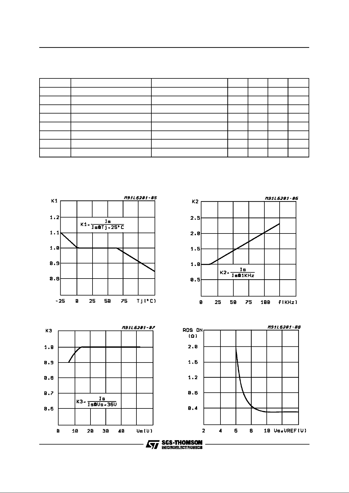
Figure 1: Typical NormalizedISvs.T
j
Figure 3: Typical NormalizedISvs. V
S
Figure2:
TypicalNormalized QuiescentCurrent
vs. Frequency
Figure4: TypicalR
DS (ON)
vs. VS~V
ref
L6201 - L6202 - L6203
5/20
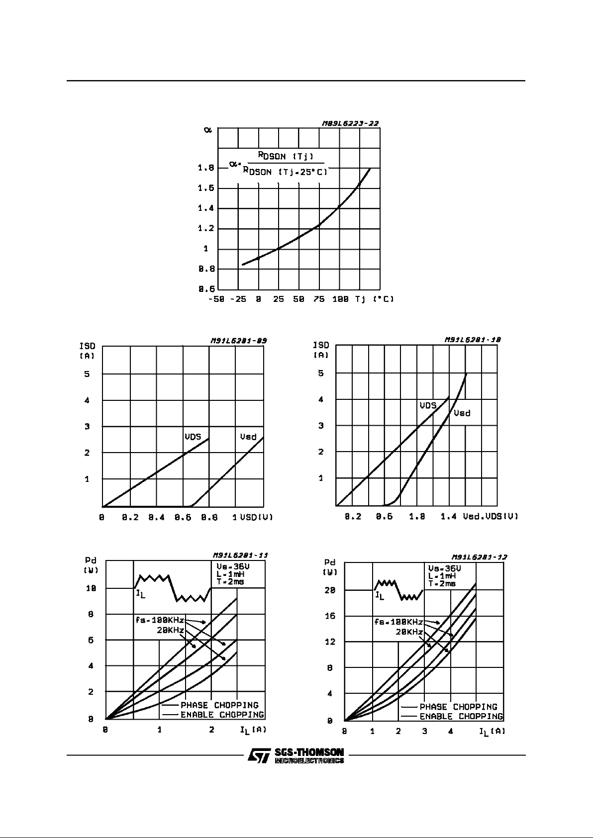
Figure 5: NormalizedR
DS (ON)
at 25°Cvs. TemperatureTypical Values
Figure6b: TypicalDiode Behaviourin Synchro-
nous Rectification (L6201PS/02/03)
Figure7b:
TypicalPower Dissipation vs I
L
(L6201PS,L6202, L6203))
Figure 6a: TypicalDiodeBehaviour in Synchro-
nous Rectification (L6201)
Figure 7a: TypicalPowerDissipation vs I
L
(L6201)
L6201 - L6202 - L6203
6/20

Figure 8a:
TwoPhase Chopping
Figure 8b:
One Phase Chopping
Figure 8c:
EnableChopping
IN1 = H
IN 2 = H
EN = H
L6201 - L6202 - L6203
7/20

TEST CIRCUITS
Figure 9: SaturationVoltage
Figure 10:
QuiescentCurrent
Figure 11: LeakageCurrent
L6201 - L6202 - L6203
8/20

Figure 12: SourceCurrent Delay Timesvs. InputChopper
Figure 13: SinkCurrent Delay Times vs. InputChopper
42V for L6201PS/02/03
42V for L6201PS/02/03
L6201 - L6202- L6203
9/20

CIRCUIT DESCRIPTION
The L6201/1PS/2/3 is a monolithic full bridge
switching motor driver realized in the new Multipower-BCD technology which allows the integration of multiple, isolated DMOS power transistors
plus mixed CMOS/bipolar control circuits. In this
way it has been possible to make all the control
inputs TTL, CMOS and µC compatible and eliminate the necessity of external MOS drive components. TheLogicDrive is shownin table 1.
Table 1
Inputs
Output Mosfets (*)
V
EN
=H
IN1 IN2
L
L
H
H
L
H
L
H
Sink 1, Sink 2
Sink 1, Source 2
Source 1, Sink 2
Source 1, Source 2
V
EN
= L X X All transistors turned oFF
L = Low H = High X = DON’tcare
(*) Numbers referred to INPUT1 or INPUT2 controlledoutput stages
Although the device guarantees the absence of
cross-conduction,the presenceof the intrinsicdiodes in the POWER DMOS structure causes the
generation of current spikeson thesensing terminals. This is due to charge-dischargephenomena
in the capacitors C1 & C2 associated with the
drain source junctions (fig. 14). When the output
switches from high to low, a current spike is generated associated with the capacitor C1. On the
low-to-high transitiona spike of the same polarity
is generated by C2, preceded by a spike of the
opposite polarity due to the charging of the input
capacity of the lower POWER DMOS transistor
(fig. 15).
TRANSISTOROPERATION
ON State
When one of the POWER DMOS transistoris ON
it can be considered as a resistor R
DS (ON)
throughout the recommendedoperating range. In
this conditionthe dissipatedpower is given by:
P
ON=RDS (ON)
⋅ I
DS
2
(RMS)
The low R
DS (ON)
of the Multipower-BCD process
can provide high currents with low power dissipation.
OFF State
When one of the POWER DMOS transistor is
OFF the V
DS
voltage is equal to the supply volt-
age and only the leakage current I
DSS
flows. The
powerdissipationduring this period is givenby:
P
OFF=VS⋅IDSS
The power dissipationis very low and is negligible
in comparison to that dissipated in the ON
STATE.
Transitions
As already seen above the transistors have an intrinsic diode between their source and drain that
can operate as a fast freewheeling diode in
switched mode applications. During recirculation
with the ENABLE input high, the voltage drop
across the transistor is R
DS (ON)
⋅ IDand when it
reaches the diode forward voltage it is clamped.
When the ENABLE input is low, the POWER
MOS is OFF and the diodecarriesall of the recirculation current. The power dissipated in the transitional times in the cycle depends upon the voltage-current waveforms and in the driving mode.
(see Fig. 7ab and Fig. 8abc).
P
trans.=IDS
(t) ⋅ VDS(t)
Figure 14:
IntrinsicStructuresin the POWER
DMOS Transistors
Figure15: CurrentTypicalSpikes on the Sens-
ing Pin
L6201 - L6202 - L6203
10/20

Boostrap Capacitors
To ensurethat the POWERDMOS transistorsare
driven correctly gate to source voltage of typ. 10
V must be guaranteed for all of the N-channel
DMOS transistors.This is easy to be provided for
the lower POWER DMOS transistors as their
sources are refered to ground but a gate voltage
greater than the supply voltage is necessary to
drive the upper transistors.This is achievedby an
internal charge pump circuit that guarantees correct DC drive in combinationwith the boostrap circuit. For efficient charging the value of the boostrap capacitor should be greater than the input
capacitance of the power transistor which is
around 1 nF. It is recommended that a capacitance of at least 10 nF is used for the bootstrap.If
a smallercapacitor is used there is a risk that the
POWER transistors will not be fully turned on and
they will show a higher RDS (ON). On the other
hand if a elevated value is used it is possible that
a currentspike may be producedin the sense resistor.
Reference Voltage
To by-pass the internal Ref. Volt. circuit it is recommendedthat a capacitorbe placed betweenits
pin and ground.A value of 0.22 µF should be sufficient for most applications. This pin is also protected against a short circuit to ground: a max.
current of 2mA max.can be sinkedout.
Dead Time
To protect the device against simultaneous conduction in both arms of the bridge resulting in a
rail to rail short circuit, the integrated logic control
provides a dead time greaterthan 40 ns.
Thermal Protection
A thermal protection circuit has been included
that will disable the deviceif the junction temperature reaches150 °C. When the temperature has
fallen to a safe level the device restarts the input
and enablesignals under control.
APPLICATION INFORMATION
Recirculation
During recirculation with the ENABLE input high,
the voltage drop across the transistor is RDS
(ON)⋅ IL, clamped at a voltage depending on the
characteristics of the source-drain diode. Although the device is protected against cross conduction, current spikes can appear on the current
sense pin due to charge/dischargephenomena in
the intrinsic source drain capacitances. In the application this does not cause any problem because the voltage spike generated on the sense
resistoris maskedby thecurrentcontrollercircuit.
Rise Time T
r
(See Fig. 16)
When a diagonal of the bridge is turned on current begins to flow in the inductive load until the
maximum current I
L
is reached after a time Tr.
The dissipated energy E
OFF/ON
is in this case :
E
OFF/ON
=[R
DS (ON)
⋅ I
L
2
⋅ Tr] ⋅ 2/3
Load Time T
LD
(See Fig.16)
During this time the energy dissipated is due to
the ON resistanceof thetransistors(E
LD
) and due
to commutation (E
COM
). As two of the POWER
DMOStransistorsare ON,E
ON
is given by :
E
LD=IL
2
⋅R
DS (ON)
⋅ 2 ⋅ T
LD
In thecommutationthe energy dissipated is :
E
COM=VS
⋅IL
⋅T
COM
⋅ f
SWITCH
⋅ T
LD
Where :
T
COM=TTURN-ON=TTURN-OFF
f
SWITCH
= Chopping frequency.
Fall Time T
f
(SeeFig. 16)
It is assumed that the energy dissipated in this
part of the cycle takes the same form as that
shownfor the rise time :
E
ON/OFF
=[R
DS (ON)
⋅ I
L
2
⋅ Tf] ⋅ 2/3
Figure 16.
L6201 - L6202- L6203
11/20

Quiescent Energy
The last contribution to the energy dissipation is
dueto the quiescentsupplycurrentand is givenby:
E
QUIESCENT=IQUIESCENT
⋅ Vs⋅ T
Total Energy PerCycle
E
TOT=EOFF/ON+ELD+ECOM
+
+E
ON/OFF+EQUIESCENT
The TotalPower Dissipation P
DIS
is simply :
P
DIS=ETOT
/T
T
r
= Rise time
T
LD
= Load drive time
T
f
=Fall time
T
d
= Deadtime
T = Period
T=T
r+TLD+Tf+Td
DC Motor Speed Control
Since theI.C. integratesa full H-Bridge in a single
package it is idealy suited for controlling DC motors. When used for DC motor control it performs
the power stage required for both speed and direction control. The device can be combinedwith
a current regulator like the L6506 to implement a
transconductance amplifier for speed control, as
shown in figure 17. In this particular configuration
only half of the L6506 is used and the other half
of the device may be used to control a second
motor.
The L6506 senses the voltage across the sense
resistor R
S
to monitor the motor current: it compares the sensed voltage both to control the
speedand duringthe brakeof the motor.
Betweenthe sense resistor and each sense input
of the L6506 a resistor is recommended; if the
connections between the outputs of the L6506
and the inputs of the L6203 need a long path, a
resistor must be added between each input of the
L6203 and ground.
A snubbernetwork made by the series of Rand C
must be foreseen very near to the output pins of
the I.C.; one diode (BYW98) is connected between each poweroutput pinand groundas well.
The following formulas can be used to calculate
the snubber values:
R ≅ V
S/lp
C=lp/(dV/dt)where:
V
S
is the maximum Supply Voltage foreseen on
the application;
I
p
is thepeak of the loadcurrent;
dv/dt is the limited rise time of the outputvoltage
(200V/µsis generallyused).
If the Power Supply Cannot Sink Current, a suitable large capacitor must be used and connected
near the supply pin of the L6203. Sometimes a
capacitorat pin 17 of the L6506let the application
better work. For motor current up to 2A max., the
L6202 can be used in a similar circuit configuration for which a typical Supply Voltage of 24V is
recommended.
Figure 17:
BidirectionalDC MotorControl
L6201 - L6202 - L6203
12/20

BIPOLARSTEPPERMOTORSAPPLICATIONS
Bipolar stepper motors can be driven with one
L6506 or L297, two full bridge BCD drivers and
very few external components. Together these
three chips form a complete microprocessor-tostepper motor interfaceis realized.
As shown in Fig. 18 and Fig. 19, the controller
connect directly to the two bridge BCD drivers.
External component are minimalized: an R.C. network to set the chopper frequency, a resistive divider (R1; R2) to establish the comparator reference voltage and a snubber network made by R
and C in series(See DCMotor SpeedControl).
Figure19: Two PhaseBipolar StepperMotor Control Circuit with Chopper CurrentControl and Translator
Figure 18: Two Phase BipolarStepper Motor Control Circuit with Chopper Current Control
L6201
L6201PS
L6202
L6203
L6201
L6201PS
L6202
L6203
L6201
L6201PS
L6202
L6203
L6201
L6201PS
L6202
L6203
L6201 - L6202- L6203
13/20

It could be requested to drive a motor at VSlower
than the minimum recommended one of 12V
(See Electrical Characteristics); in this case, by
accepting a possible small increas in the R
DS (ON)
resistance of the power output transistors at the
lowest Supply Voltage value, may be a good solution the one shownin Fig. 20.
THERMAL CHARACTERISTICS
Thanks to the high efficiency of this device, often
a true heatsink is not needed or it is simply obtained by means of a copper side on the P.C.B.
(L6201/2).
Under heavy conditions, the L6203 needs a suitable cooling.
By using two square copper sidesin a similarway
as it shown in Fig. 23, Fig. 21 indicates how to
choose the on board heatsink area when the
L6201 totalpower dissipationis knownsince:
R
Th j-amb
=(T
j max.–Tamb max
)/P
tot
Figure 22 shows the Transient Thermal Resistance vs. a singlepulse time width.
Figure 23 and 24 referto the L6202.
For the Multiwatt L6203 addition information is
given by Figure25 (ThermalResistance JunctionAmbient vs. Total Power Dissipation) and Figure
26 (Peak Transient Thermal Resistance vs. Repetitive Pulse Width) while Figure 27 refersto the
single pulseTransientThermalResistance.
Figure 20: L6201/1P/2/3Used at a Supply Volt-
age RangeBetween 9 and 18V
Figure21:
TypicalR
Th J-amb
vs. ”OnBoard”
HeatsinkArea (L6201)
Figure22: TypicalTransientR
TH
in SinglePulse
Condition(L6201)
Figurre23:
TypicalR
Th J-amb
vs. Two ”On Board”
SquareHeatsink (L6202)
L6201
L6201PS
L6202
L6203
L6201 - L6202 - L6203
14/20

Figure 24
: TypicalTransient Thermal Resistance
for SinglePulses (L6202)
Figure25: TypicalR
Th J-amb
of Multiwatt
Packagevs. Total PowerDissipation
Figure 26: TypicalTransientThermal Resistance
for SinglePulses with and without
Heatsink(L6203)
Figure27:
TypicalTransientThermal Resistance
versusPulse Width and Duty Cycle
(L6203)
L6201 - L6202- L6203
15/20

POWERDIP18PACKAGE MECHANICAL DATA
DIM.
mm inch
MIN. TYP. MAX. MIN. TYP. MAX.
a1 0.51 0.020
B 0.85 1.40 0.033 0.055
b 0.50 0.020
b1 0.38 0.50 0.015 0.020
D 24.80 0.976
E 8.80 0.346
e 2.54 0.100
e3 20.32 0.800
F 7.10 0.280
I 5.10 0.201
L 3.30 0.130
Z 2.54 0.100
L6201 - L6202 - L6203
16/20

SO20 PACKAGE MECHANICAL DATA
DIM.
mm inch
MIN. TYP. MAX. MIN. TYP. MAX.
A 2.65 0.104
a1 0.1 0.3 0.004 0.012
a2 2.45 0.096
b 0.35 0.49 0.014 0.019
b1 0.23 0.32 0.009 0.013
C 0.5 0.020
c1 45 (typ.)
D 12.6 13.0 0.496 0.512
E 10 10.65 0.394 0.419
e 1.27 0.050
e3 11.43 0.450
F 7.4 7.6 0.291 0.299
L 0.5 1.27 0.020 0.050
M 0.75 0.030
S 8 (max.)
L6201 - L6202- L6203
17/20

e
a2
A
E
a1
PSO20MEC
DETAILA
T
D
110
1120
E1
E2
hx45°
DETAILA
lead
slug
a3
S
Gage Plane
0.35
L
DETAILB
R
DETAILB
(COPLANARITY)
GC
-C-
SEATING PLANE
e3
b
c
NN
PowerSO20PACKAGE MECHANICAL DATA
DIM.
mm inch
MIN. TYP. MAX. MIN. TYP. MAX.
A 3.60 0.1417
a1 0.10 0.30 0.0039 0.0118
a2 3.30 0.1299
a3 0 0.10 0 0.0039
b 0.40 0.53 0.0157 0.0209
c 0.23 0.32 0.009 0.0126
D (1) 15.80 16.00 0.6220 0.6299
E 13.90 14.50 0.5472 0.570
e 1.27 0.050
e3 11.43 0.450
E1 (1) 10.90 11.10 0.4291 0.437
E2 2.90 0.1141
G 0 0.10 0 0.0039
h 1.10
L 0.80 1.10 0.0314 0.0433
N10
°
(max.)
S8
°
(max.)
T 10.0 0.3937
(1) ”D and E1”do not include mold flashor protrusions
- Moldflashor protrusions shall not exceed 0.15mm(0.006”)
L6201 - L6202 - L6203
18/20

MULTIWATT11 PACKAGE MECHANICAL DATA
DIM.
mm inch
MIN. TYP. MAX. MIN. TYP. MAX.
A 5 0.197
B 2.65 0.104
C 1.6 0.063
D 1 0.039
E 0.49 0.55 0.019 0.022
F 0.88 0.95 0.035 0.037
G 1.57 1.7 1.83 0.062 0.067 0.072
G1 16.87 17 17.13 0.664 0.669 0.674
H1 19.6 0.772
H2 20.2 0.795
L 21.5 22.3 0.846 0.878
L1 21.4 22.2 0.843 0.874
L2 17.4 18.1 0.685 0.713
L3 17.25 17.5 17.75 0.679 0.689 0.699
L4 10.3 10.7 10.9 0.406 0.421 0.429
L7 2.65 2.9 0.104 0.114
M 4.1 4.3 4.5 0.161 0.169 0.177
M1 4.88 5.08 5.3 0.192 0.200 0.209
S 1.9 2.6 0.075 0.102
S1 1.9 2.6 0.075 0.102
Dia1 3.65 3.85 0.144 0.152
L6201 - L6202- L6203
19/20

Information furnished is believed to be accurate and reliable. However, SGS-THOMSON Microelectronics assumes no responsibility for the
consequences of use of such information nor for any infringement of patents or other rights ofthird partieswhich may result from its use. No
license is granted by implication or otherwise under any patent or patentrights of SGS-THOMSON Microelectronics. Specification mentioned
in this publication are subject to change withoutnotice. This publication supersedes and replaces all information previously supplied. SGSTHOMSON Microelectronics products are not authorized for use as critical components in life support devices or systems without express
written approval of SGS-THOMSON Microelectronics.
1997SGS-THOMSON Microelectronics– PrintedinItaly – AllRightsReserved
SGS-THOMSON Microelectronics GROUPOF COMPANIES
Australia - Brazil - Canada- China - France - Germany - Hong Kong - Italy - Japan - Korea - Malaysia - Malta - Morocco - The Netherlands -
Singapore - Spain - Sweden - Switzerland- Taiwan - Thailand- UnitedKingdom - U.S.A.
L6201 - L6202 - L6203
20/20
 Loading...