

L6180
L6181
OCTAL LINE RECEIVER
ADVANCE DATA
OCTAL LINE RECEIVERFOR:
- EIA STD RS232D
RS423A
RS422A
- CCIT V.10
V.11
V.28
X.26
NO EXTERNALCOMPONENTS
INPUTFAIL SAFING CAPABILITY
HIGHCROSSTALKREJECTION
L6180 DATA RATE < 100KBIT/S
L6181 DATA RATE < 1MBIT/S
50V EOS OUTPUTPROTECTION
DESCRIPTION
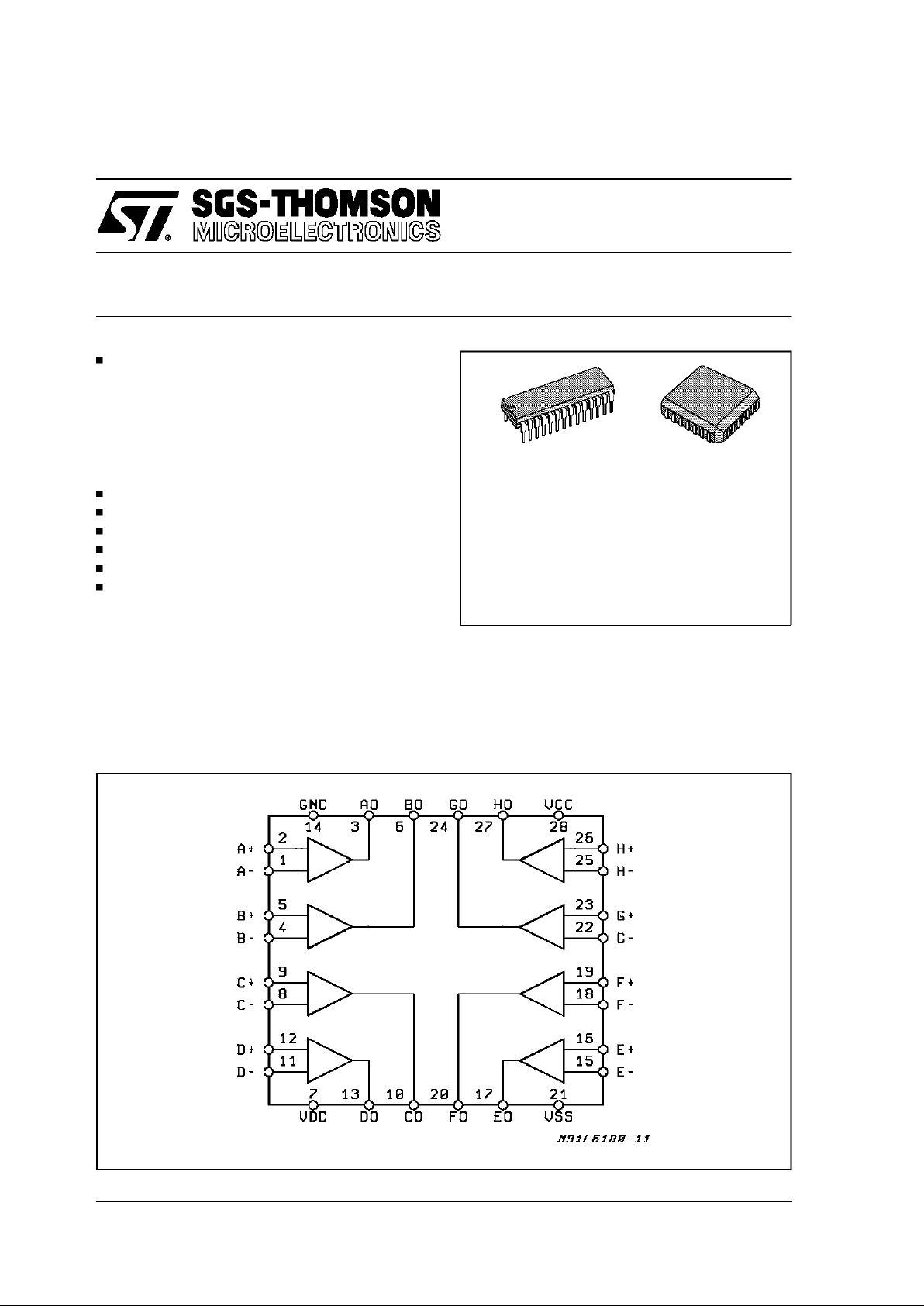
L6180/1 is an octal line receiver in a plastic DIP
or PLCC designed to meet a wide range of digital
communications requirements as outlined in the
EIA standards RS232A without additional components, as well as the low speed applications of
RS422A.
The receiver meets the CCIT recommendations
V.10, V.11, X.26and V.28 low speed applications
(below100KBS).
A low pass filter on the input starts to roll off at a
frequencyof 100KHz.
This is advancedinformation on a new product now in developmentor undergoing evaluation. Details are subject to change without notice.
October 1993
BLOCK DIAGRAM
ORDERING NUMBER: L6180ADIP 28
L6180D PLCC28
L6181A DIP 28
L6181D PLCC28
DIP 28
PLCC 28
1/10
ABSOLUTE MAXIMUM RATINGS
Symbol Parameter Value Unit
V
CC
SupplyVoltage 7 V
V
DD SupplyVoltage 13.5 V
V
SS
LogicSupply Voltage -13.5 V
C
RR Common Mode Range ±15 V
V
ID
DifferentialInput Voltage ±25 V
P
tot Power Dissipation (PLCC 28) 800 mW
Power Dissipation (DIP 28) 1200 mW
I
OS Output Sink Current 50 mA
t Output Short Circuit Time 1 sec
T
op Operating Free Air Temperature Range 0 to 70 °C
T
stg Storage Temperature Range -65 to 150 °C
ESD 2KV max ESD 50µJ
InputTransient Protection 50V min EOS 100µs
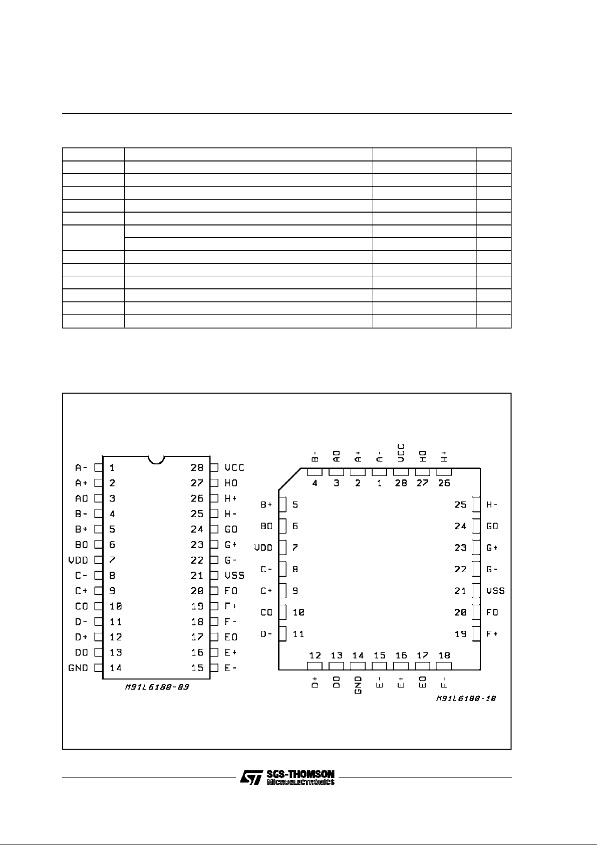
PIN CONNECTIONS(Top views)
DIP28 PLCC28
L6180 - L6181
2/10
ELECTRICALCHARACTERISTICS (VCC =5V±5%;VCM = -7 to 7V; Tamb = 0 to 70°C;
V
SS
= -9 to 13.5V; VDD= 9 to13.5V; unless otherwisespecified.)
Symbol Parameter Test Condition Min. Typ. Max. Unit
V
IN
Input Current (See Fig.1 and note2)
V
CC = 0 to 5.25V;
V
SS,VDD = 0 to 13.5V
V
IN = - 10 to 10V
V
IN = - 15 to 15V
±3
±4.25mAmA
R
I Input Resistance VIA or VIB = 3 to 15V; (see fig.1)
R
I
=
[(V
IA
or VIN)−V
IOC
]
I
IN
37KΩ
V
FS
Failsafe Output Voltage IO = -440µA (See Fig.3) 2.7 V
V
OH
High Level Output Voltage VCC = 4.75V; VID = -1V;
I
OH = -440µA
2.7 V
V
OL
Low Level Output Voltage VCC = 5.25V; VID = -1V;
I
OL = 2mA
0.4 V
V
IT2
V
IOH
ComparatorThreshold
Voltage
(See Fig.4) 1.8 2.2 2.6 V
I
IH2
High Operating Threshold
Voltage
VOL = 0.4V; IOL =2mA;
(See Fig.4)
-25 -75 mV
I
IH1
Low Operating Threshold
Voltage
VOH = 2.7V; IO = -440µA
(See Fig.4)
-125 -175 mV
V
H
Input Hysteresis Voltage |VTH2 -VTH1| 50 150 mV
V
IOC1
Open Circuit Input Voltage Measured in accordance with
V.28 and RS-232D
(see note 4 and 7)
0.6 2 V
V
IOCH
Open Circuit Input Voltage Measured in presence of AC
Input Signal (see note 7)
3.5 4 4.5 V
I
OS
Open Short Circuit Current VCC = 5.25V; VO =0;VID = 1V;
(see note 5)
20 100 mA
V
IBV
Input for Balance Test (see Figure 7 and note 11) 0.4 V
C
I
Input Capacitance 100 pF
V
CC
Supply Current VCC =4.75V to 5.25V;(seenote6) 100 mA
V
dd
Supply Current Vdd = 9 to 3.5V; (see note 6) 30 mA
V
SS
Supplyt Current VSS = -9 to 13.5V;(see note 6) 30 mA
I
OS
Open Short Circuit Current VCC = 5.25V; VO =0;VID = 1V;
(see note 5)
20 100 mA
T
plh
Propagation Delay Low to High RL = 390Ω;CL= 50pF;
|V
IN = 1V|; (see fig 5 test Circuit
Fig. 6)
0 1500 ns
T
phl
Propagation Delay Low to High RL = 390Ω;CL= 50pF;
|V
IN = 1V|; (see fig 5 test Circuit
Fig. 6)
0 1500 ns
V
IOCH
Delay VIOCL to VIOCH Switching (see note 7A) 5 ms
V
IOCL
Delay VIOCH to VIOCL Switching (see note 7B) 200 ms
V
ist
|Tplh -Tphl|RL= 390Ω;CL= 50pF;
|V
IN| = 1V;(see fig. 5; Test
Circuit Fig. 6)
0 500 ns
T
SKEW1
Skew between rec’s in PKg Tp
(1) hl/1h - Tp (2) hl/1h
RL = 390Ω;CL= 50pF;
|V
IN| = 1V;(see fig. 5; Test
Circuit Fig. 6)
0 300 ns
f
A
Frequency Accepted
(Receiver will Output)
VIN = 200mVpp; (see fig. 8 and
note 7;
100 KHz
L6180 - L6181
3/10

ELECTRICALCHARACTERISTICS (VCC =5V±5%; VCM = -7 to 7V; Tamb = 0 to 70°C;
V
SS
= -9 to 13.5V; VDD= 9 to13.5V; unless otherwisespecified.)
Symbol Parameter Test Condition Min. Typ. Max. Unit
f
R
Frequency Rejected
(No Receiver Output)
VIN = 2Vpp;
(see fig. 8 and note 7)
5 MHz
Note:
1) The algebric convention, where the less positive (more negative) is designedthe minimum
2) With the voltage V
IA or (VIB) ranging between ±15V, while VIB or (VIA)is openor grounded, the resultant input current IIA or (IIB) shall remain
within the shaded region shown in the graph in Fig.1.
3) Either Point B’ or Point A’ is grounded in Figure 1
4) V
ICC measured from grounded to (+) input with (-) input grounded
V
ICC measured from grounded to (+) inputwith (-)input grounded
5) Not more than oneoutput should be shorted at a time and forless than 1 seond
6) The sum of the product of the maximum supply currents and voltages cannot exceed themaximum power dissipation
7) A: The conditions for the inpit switching from V
IOCL to VIOCH mode is: Vid in start bit ”spacing condition”for less than TpVioch (5ms).
B: The conditions for the input switching from V
IOCH to VIOCL mode is: Vid > WW2 for greater than TpVIOCL (200ms)
8) An example of a frequencyresponse plot meeting the rejection/acceptance requirements is provided in figure 8.
LINE TRANSIENT IMMUNITY (Considering the following cases; powered ON, Powered OFF-LOW impedancepower supplyand powered OFF-HIGHimpedancesupply)
Symbol Parameter Test Condition Min. Typ. Max. Unit
ESD Static tested per MIL-STD-883
(see note 9)
2KV
EOS Stress transient pulse both polarities
for 100µs (see note 9 and Fig. 2)
50 V
Note:
9) Allpins are required to withstand this parameters.
10) Input pins are required to withstand fig.2 without any degradation tothe circuit.
11) The balance test requirement can be met by use of a currentlimit circuit which reduces theinput bias current I
ib (see figure 7)
for input voltages below a threshold voltage given by (I
ib x 1K)- 400mV.
Figure1: Input CurrentVoltage Mesurements
L6180 - L6181
4/10

Figure3: Output Failsafing
Figure2: EOSRequiremets
The output assumes a logic ”1”under the followingconditions, (see figure 3)
1 Bothinputs open
2 Both inputsshorted
3 SignalOpencircuit
3a Commongrounded, signal open circuit
4 Common open,generator powered-on
5 Generatorpowered-down (seenote 7)
6 Common open,generator powered-down
6a Signal grounded,common open, generator powered-down
7 Lessthan 250mVpp differential signal
L6180 - L6181
5/10

Figure4: Thresholdvoltage definition
Figure5: PropagationDelay
Figure6: AC Test Circuit
L6180 - L6181
6/10

INPUTBALANCE MEASUREMENT
The balance of the receiver input voltage-current
characteristics and bias voltages shall be such
that the receiverwill remainin theintendedbinary
state when a differential voltage Vi of 400mV is
appliedthrough 500Ω ±1% to each input terminal,
as shown above, and Vcm is varied between -7
and +7V.
When the polarity of Vi is reversed, the opposite
binary state shall be maintained under the same
conditions. Maintain input balance with input B
commonwith another receiver.
The voltage input (V
IN) rejection is checked at the
center point between the High Operating Threshold (V
th2) and theLow OperatingThreshold(Vth1)
Figure7: Receiverinput Balance Measurement
Figure8: HighFrequencySignalRejection
L6180 - L6181
7/10

PLCC28PACKAGE MECHANICAL DATA
DIM.
mm inch
MIN. TYP. MAX. MIN. TYP. MAX.
A 12.32 12.57 0.485 0.495
B 11.43 11.58 0.450 0.456
D 4.2 4.57 0.165 0.180
D1 2.29 3.04 0.090 0.120
D2 0.51 0.020
E 9.91 10.92 0.390 0.430
e 1.27 0.050
e3 7.62 0.300
F 0.46 0.018
F1 0.71 0.028
G 0.101 0.004
M 1.24 0.049
M1 1.143 0.045
L6180 - L6181
8/10

DIP28 PACKAGEMECHANICAL DATA
DIM.
mm inch
MIN. TYP. MAX. MIN. TYP. MAX.
a1 0.63 0.025
b 0.45 0.018
b1 0.23 0.31 0.009 0.012
b2 1.27 0.050
D 37.34 1.470
E 15.2 16.68 0.598 0.657
e 2.54 0.100
e3 33.02 1.300
F 14.1 0.555
I 4.445 0.175
L 3.3 0.130
L6180 - L6181
9/10

Information furnished is believed to be accurate and reliable. However, SGS-THOMSON Microelectronics assumes no responsibility for the
consequences of use of such information nor for any infringement ofpatents or other rights of third parties which may result from its use. No
license is granted by implication or otherwise under any patent or patent rights of SGS-THOMSON Microelectronics. Specifications mentioned in this publication are subject to change without notice. This publication supersedes and replaces all information previously supplied.
SGS-THOMSON Microelectronics products are not authorized for use as critical components in life support devices or systems without express written approval of SGS-THOMSON Microelectronics.
1995 SGS-THOMSON Microelectronics - All RightsReserved
SGS-THOMSON Microelectronics GROUPOF COMPANIES
Australia - Brazil - France - Germany - Hong Kong - Italy - Japan- Korea - Malaysia -Malta - Morocco - The Netherlands - Singapore -
L6180 - L6181
10/10
 Loading...