

L6114
L6115
QUAD 100 V, DMOS SWITCH
.OUTPUTVOLTAGETO 100 V
.0.7 ΩR
DS(ON)
.SUPPLYVOLTAGEUP TO 60 V
.LOWINPUT CURRENT
.TTL/CMOSCOMPATIBLEINPUTS
.HIGHSWITCHING FREQUENCY (200 KHz)
DESCRIPTION
Realized with the Multipower-BCD mixed bipolar/CMOS/DMOSprocess,theL6114/15monolithic
quad DMOS switch is designed for high current,
highvoltageswitching applications.Eachofthefour
switchesiscontrolledbyalogicinputand allfourare
controlledby a common enableinput. Allinputsare
TTL/CMOScompatiblefordirectconnectiontologic
circuits.Eachsourceis availablefor theinsertionof
the senseresistorsin current controlapplications.
Two versionsare available: theL6114 mountedin
aPowerdip14+3+3packageandtheL6115in a15leadMultiwattpackage.
MULTIP OWER BCD TE CHNOLOGY
Powerdip 14 + 3 + 3
Multiwatt-15
ORDE R I NG NUMBE RS : L6114 (P ower d ip)
L6115 (Mult iwatt- 15)
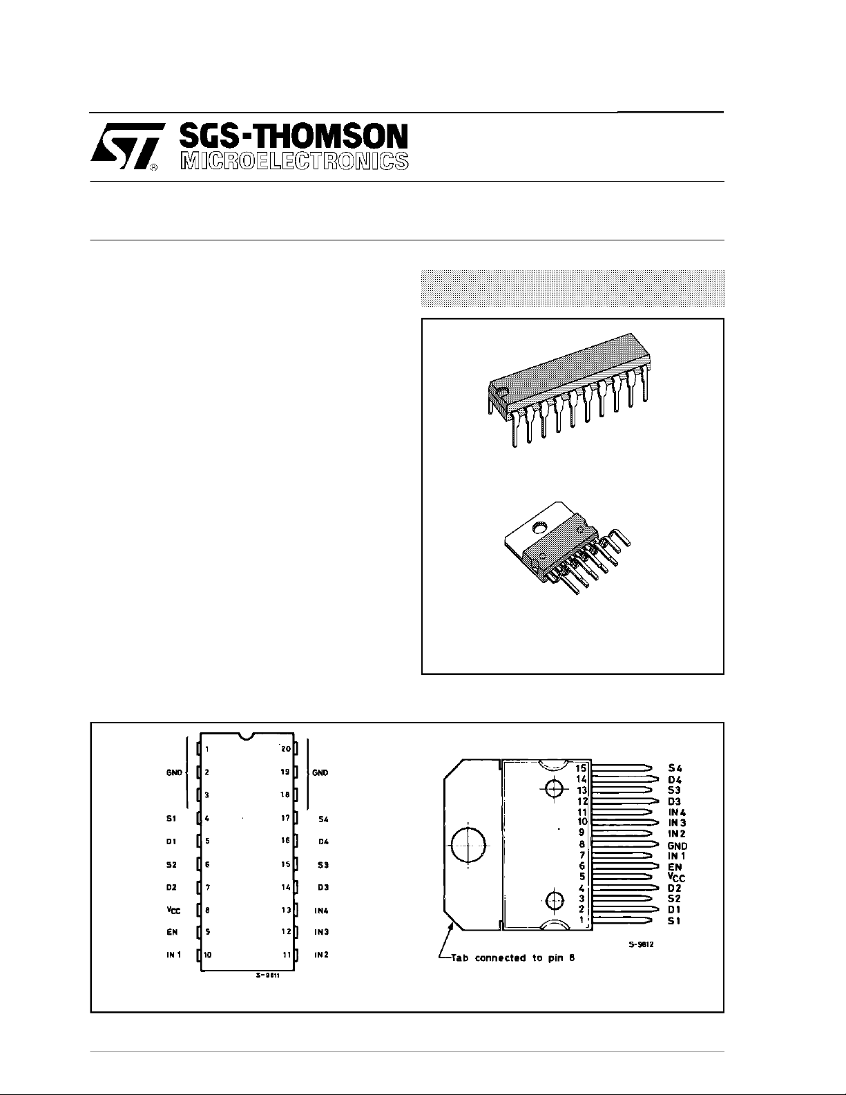
PIN CONNECTIONS (top view)
L6114 (Powerdip)
April1993
L6115 (Mul t i w att-15)
1/11
L6114 - L6115
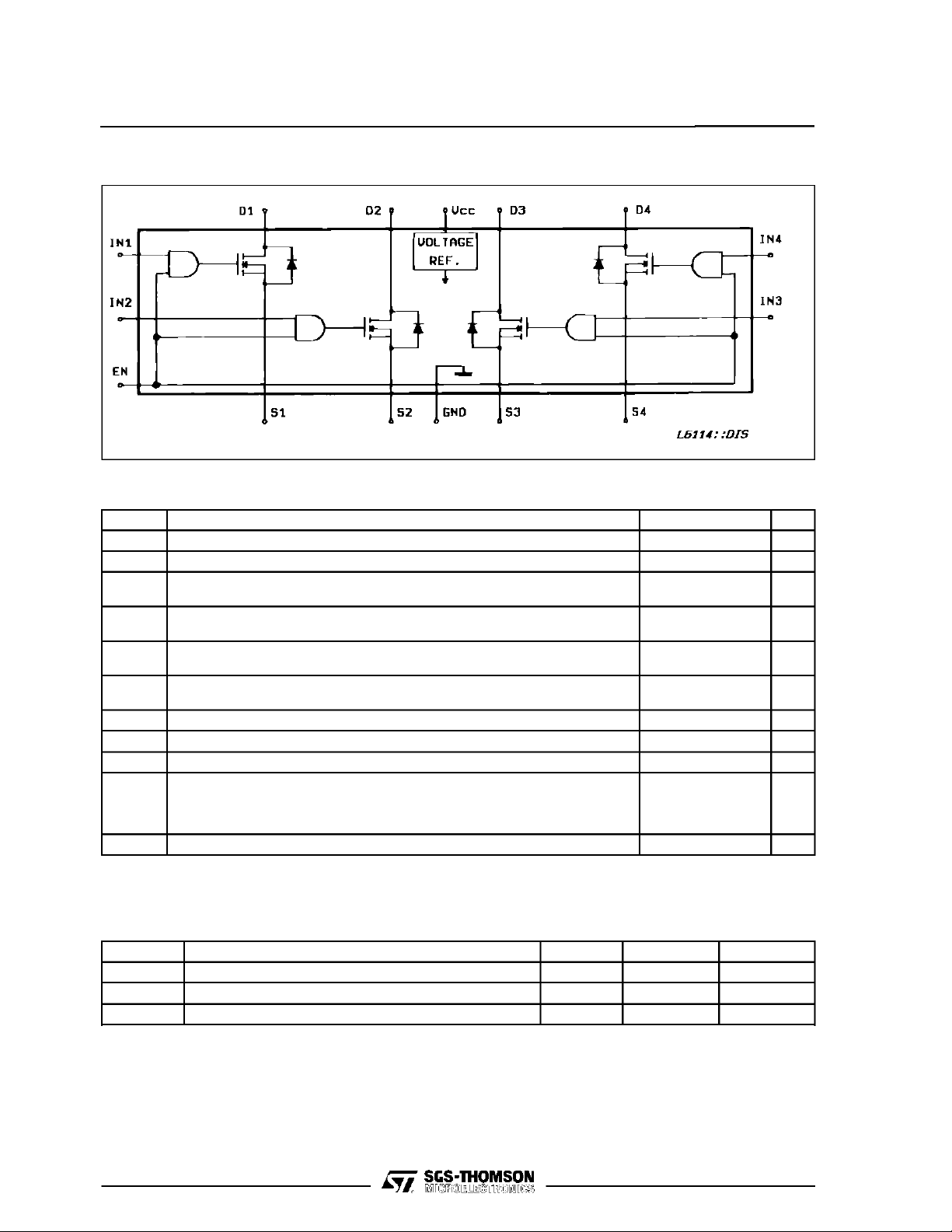
BLOCK DIAGRAM
ABSOLUTE MAXIMUM RATINGS
Symbol Parameter Value Unit
V
V
I
DM
I
I
SDM
V
V
V
P
T
stg,Tj
(*) Pulse width ≤ 300 µs,dutycycle ≤ 10%.
Note : I
Drain-source Voltage 100 V
DS
Supply Voltage 60 V
CC
Continuous Drain Current @<0>T
I
D
@<0>T
pins
case
=90°C
=90°C
Powerdip
Multiwatt –15
(*) Pulsed Drain Current Powerdip
Multiwatt –15
Continuous Source-drain
SD
Diode Current
@<0>T
@<0>T
pins
case
=90°C
=90°C
Powerdip
Multiwatt –15
Pulsed Source Drain Diode Current Powerdip
Multiwatt –15
Input Voltage 7V
IN
Enable Voltage 7V
EN
Source Voltage – 1 to + 4 V
S
Total Power Dissipation @ T
tot
@T
@T
@T
pins
case
amb
amb
=90°C
=90°C
=70°C
=70°C
Powerdip
Multiwatt –15
Powerdip
Multiwatt –15
1.5
3
5
8
1.5
3
5
8
4.3
20
1.3
2.3
Storage and Junction Temperature Range – 40 to + 150 °C
D,IDM,ISD,ISDM
aregiven per channel.
A
A
A
A
A
A
A
A
W
W
W
W
THERMAL DATA
Symbol Parameter Powerdip Multiwatt–15 Unit
Thermal Resistance Junction-pins Max. 14 Thermal Resistance Junction-case Max. - 3
Thermal Resistance Junction-ambient Max. 65 35
2/11
R
th j-pins
R
th j-case
R
th j-amb
o
C/W
o
C/W
o
C/W
L6114 - L6115
ELECTRICAL CHARACTERISTICS (Tj=25oC, VCC= 40V, unless otherwise specified)
Symbol Parameter Test Conditions Min. Typ. Max. Unit
V
CC
I
CC
I
Q
BV
DSS
I
DSS
R
DS (on)
V
IN L,VEN L
V
IN H,VEN H
I
IN L,IEN L
I
IN H,IEN H
t
d (on)
t
r
t
d (off)
t
f
V
SD
V
SD (on)
(*) Pulse test : pulse width = 300 µs, dutycycle = 2 %.
Supply Voltage 14 48 V
Supply Current All VIN=H
= Square Wave
V
EN
(200kHz, 50 % DC)
9mA
Quiescent Current VEN=L 2 3 mA
Drain Source Breakdown Voltage ID= 1mA, VEN= L 100 V
Output Leakage Current VEN=L
= 100V
V
DS
= 80V, Tj= 125°C1
V
DS
(*) Static Drain-source on Resistance VCC≥ 14V, ID= 1.5A
EN,VIN
=H
V
0.7 Ω
1
Input Low Voltage – 0.3 0.8 V
Input High Voltage 2 7 V
Input Low Current VIN,VEN= L – 100 µA
Input High Current VIN,VEN=H 10 µA
Turn on Delay Time
= 1.5A
I
Rise Time 100 ns
Turn off Delay Time 400 ns
D
See Test Circuit and
Waveforms
300 ns
Fall Time 100 ns
(*) Source Drain Diode Forward Voltage ISD= 1.5A, VEN= L 1.5 V
(*) Source Drain Forward Voltage ISD= 1.5A - VIN,VEN= H 1.2 V
mA
3/11
L6114 - L6115
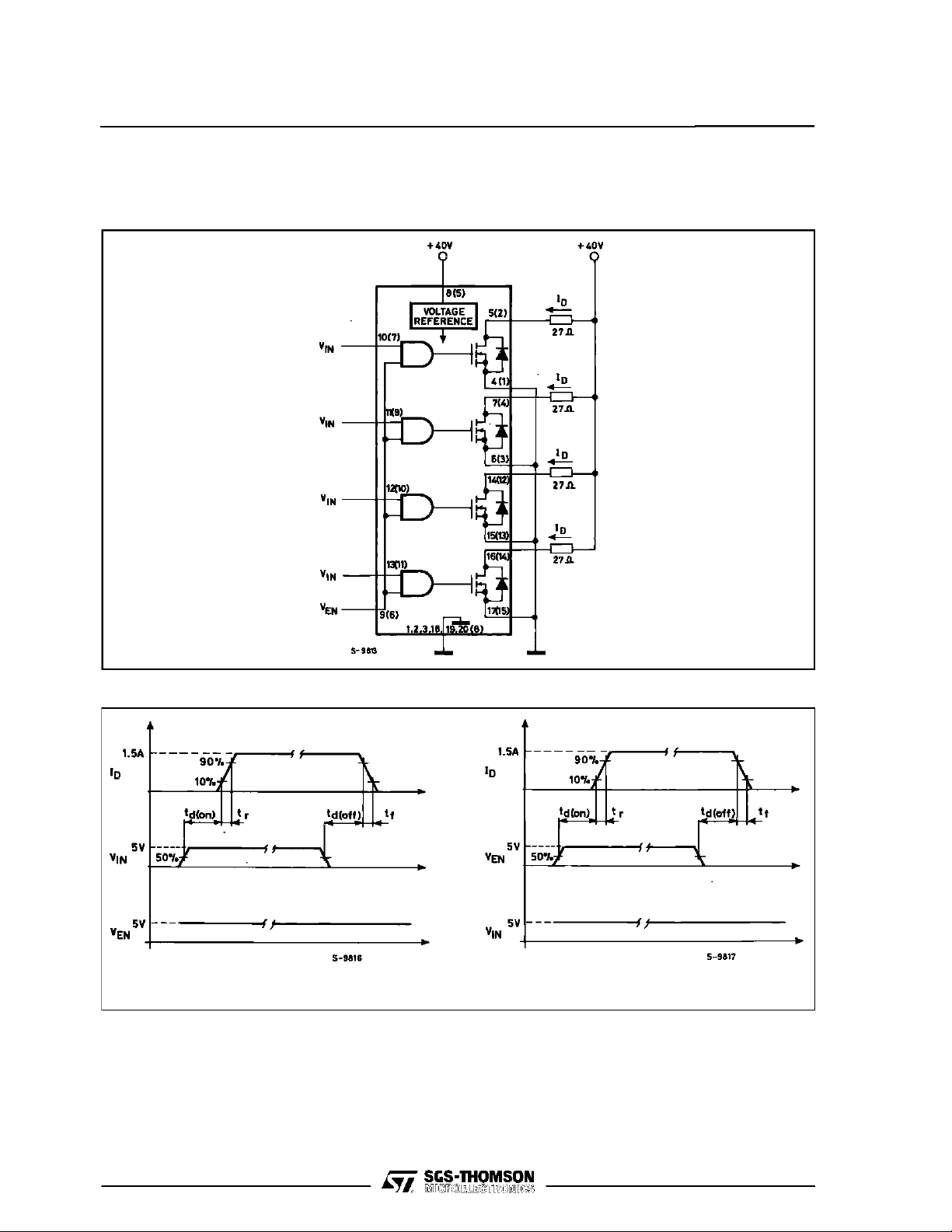
SWITCHING TI ME S RE S I STIVE L O AD
Figure 1 : Test Circuit
(Pinsx = Powerdip ; Pins (x) =Multiwatt).
Figure 2 : Waveforms.
b)a)
4/11

TEST CIRCUIT (Pins x = Powe rdip ; Pins (x) = Multiwatt)
L6114 - L6115
Figure 3 : QuiescentCurrent and Output
LeakageCurrent..
V
= 0.8 V
EN
Figure4 : SupplyCurrent.
V
=2V
IN
= squarewave{f = 200 KHz
V
EN
DC= 50%
Figure 5 : R
. Figure6 : Source-drainDiodeForward Voltage.
DS (on)
VCC=14V, VIN= 2 V, VEN=2V
I
=square wave, f = 3 KHz DC = 2 %
D
(*)V
is taken during the time in which the
DS
ID=1.5 A RDS=
=2 V, ISDsquarewave, f = 3 KHz DC= 2 %
V
IN
V
1.5
DS
Set VEN=0.8 V for VSD(takenduring the time in which
-
I
= 1.5 A)
SD
Set VEN=2 Vfor V
-
I
= 1.5 A)
SD
(takenduring thetime inwhich
SD (on)
5/11

L6114 - L6115
Figure 7 : Input LogicLevels
Set V= 0.8V S1,S2open for I
Set V= 0.8V S1,S2close for V
Set V= 2 V S1,S2open for I
Set V= 2 V S1,S2close for V
IN L
IN L
IN H
IN H
and I
and V
andI
andV
EN L
EN H
EN H
EN H
Figure 8 : StaticDrain-source on Resistance. Figure9 : Normalized Break-downVoltagevs.
Temperature.
6/11

L6114 - L6115
Figure10 : Normalizedon Resistancevs.
Temperature.
Figure12 : R
vs.Dissipated Power(Multiwatt).
thj-amb
Figure11 : Typical Source-drainDiodeForward
Voltage.
(*) Rth≈ 9 °C/W.
7/11

L6114 - L6115
Figure 13 : TransientThermal Resistancefor SinglePulses(Multiwatt).
Figure 14 : PeakTransientThermalResistancevs.Pulse width and duty cycle(Multiwatt).
8/11

POWERDIP20PACKAGE MECHANICAL DATA
L6114 - L6115
DIM.
MIN. TYP. MAX. MIN. TYP. MAX.
a1 0.51 0.020
B 0.85 1.40 0.033 0.055
b 0.50 0.020
b1 0.38 0.50 0.015 0.020
D 24.80 0.976
E 8.80 0.346
e 2.54 0.100
e3 22.86 0.900
F 7.10 0.280
I 5.10 0.201
L 3.30 0.130
Z 1.27 0.050
mm inch
9/11

L6114 - L6115
MULTIWATT15 PACKAGEMECHANICAL DATA
DIM.
A 5 0.197
B 2.65 0.104
C 1.6 0.063
D 1 0.039
E 0.49 0.55 0.019 0.022
F 0.66 0.75 0.026 0.030
G 1.14 1.27 1.4 0.045 0.050 0.055
G1 17.57 17.78 17.91 0.692 0.700 0.705
H1 19.6 0.772
H2 20.2 0.795
L 22.1 22.6 0.870 0.890
L1 22 22.5 0.866 0.886
L2 17.65 18.1 0.695 0.713
L3 17.25 17.5 17.75 0.679 0.689 0.699
L4 10.3 10.7 10.9 0.406 0.421 0.429
L7 2.65 2.9 0.104 0.114
M 4.2 4.3 4.6 0.165 0.169 0.181
M1 4.5 5.08 5.3 0.177 0.200 0.209
S 1.9 2.6 0.075 0.102
S1 1.9 2.6 0.075 0.102
Dia1 3.65 3.85 0.144 0.152
MIN. TYP. MAX. MIN. TYP. MAX.
mm inch
10/11

L6114 - L6115
Information furnished is believed to be accurate and reliable. However, SGS-THOMSON Microelectronics assumes no responsibility for
the consequences of use of such information nor for any infringement of patents or other rights of third parties which may result from its
use. No license is granted by implication or otherwise under any patent or patent rights of SGS-THOMSON Microelectronics. Specifications mentioned in this publication are subject to change without notice. This publication supersedes and replaces all information previously supplied. SGS-THOMSON Microelectronics products are not authorized for use as critical components in life support devices or
systems withoutexpress written approval of SGS-THOMSON Microelectronics.
1994 SGS-THOMSON Microelectronics - All Rights Reserved
MULTIWATT is a Registered Trademark of SGS-THOMSON Microelectronics
Australia - Brazil - France- Germany - Hong Kong - Italy - Japan - Korea - Malaysia - Malta - Morocco - The Netherlands - Singapore -
SGS-THOMSON Microelectronics GROUP OF COMPANIES
Spain - Sweden - Switzerland - Taiwan - Thaliand - United Kingdom - U.S.A.
11/11
 Loading...