

L601-L603
L602-L604
DARLINGTONARRAYS
EIGHTDARLINGTONSPERPACKAGE
OUTPUTCURRENT400 mAPERDRIVER(500
mAPEAK)
OUTPUTVOLTAGE 90 V (V
CE (sus))
=70V)
INTEGRAL SUPPRESSION DI ODES FOR
INDUCTIVE LOADS
OUTPUTS CAN BE PA RALLELED FOR
HIGHERCURRENT
TTL / CMOS / PMOS / DTL COMPATIBLE
INPUTS
INPUTS PINNED OPPOSITE OUTPUTS TO
SIMPLIFYLAYOUT
DESCRIPTION
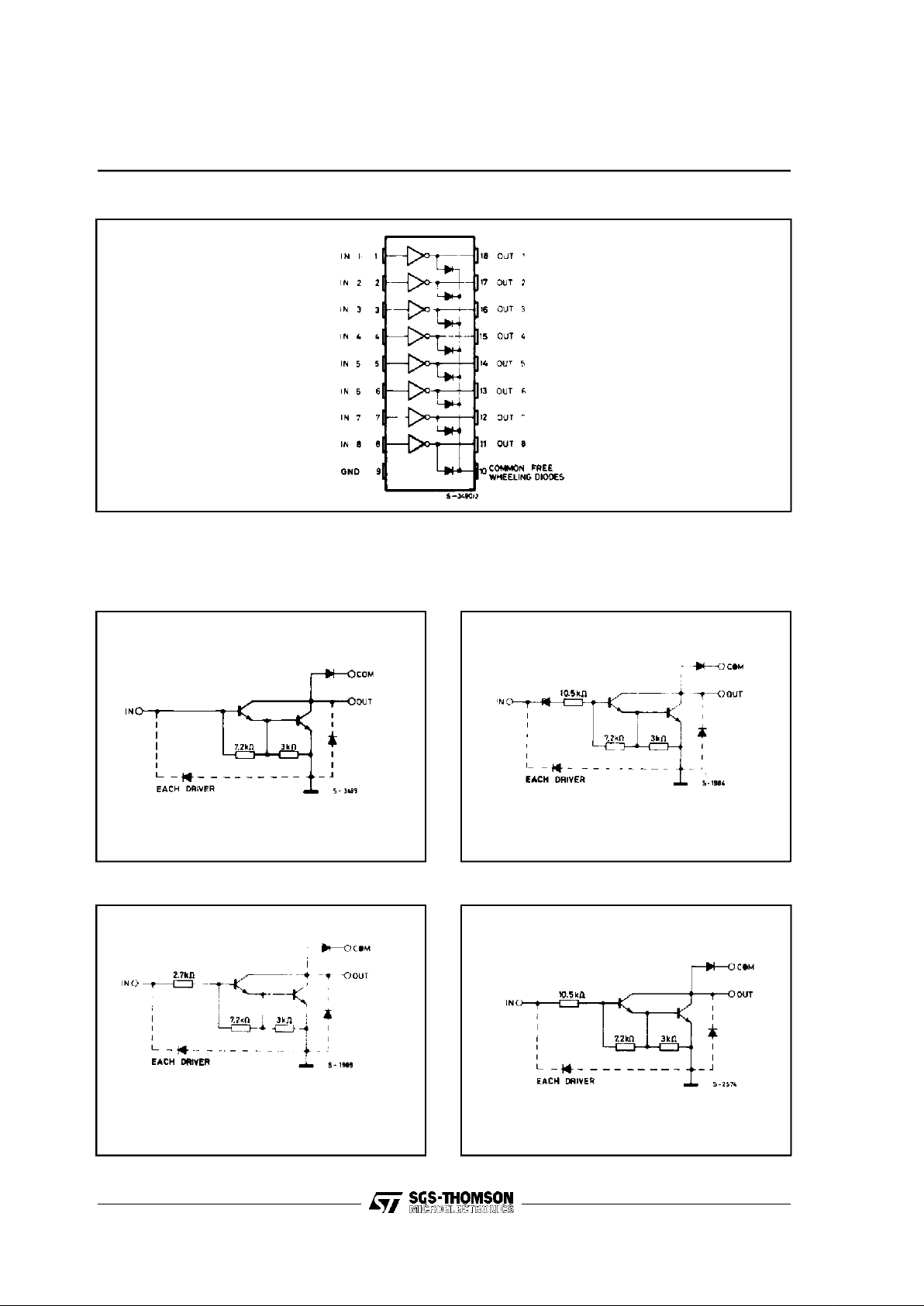
The L601, L602,L603 and L604 are high voltage,
high current darlington arrays each containing
eight open collectordarlingtonpairs with common
emitters. Eachchannel isratedat 400 mAand can
with stand peak currents of 500 mA. Suppression
diodes are included for inductive load drivingand
the inputs are pinnedopposite the outputs to simplifyboard layout.
October 1991
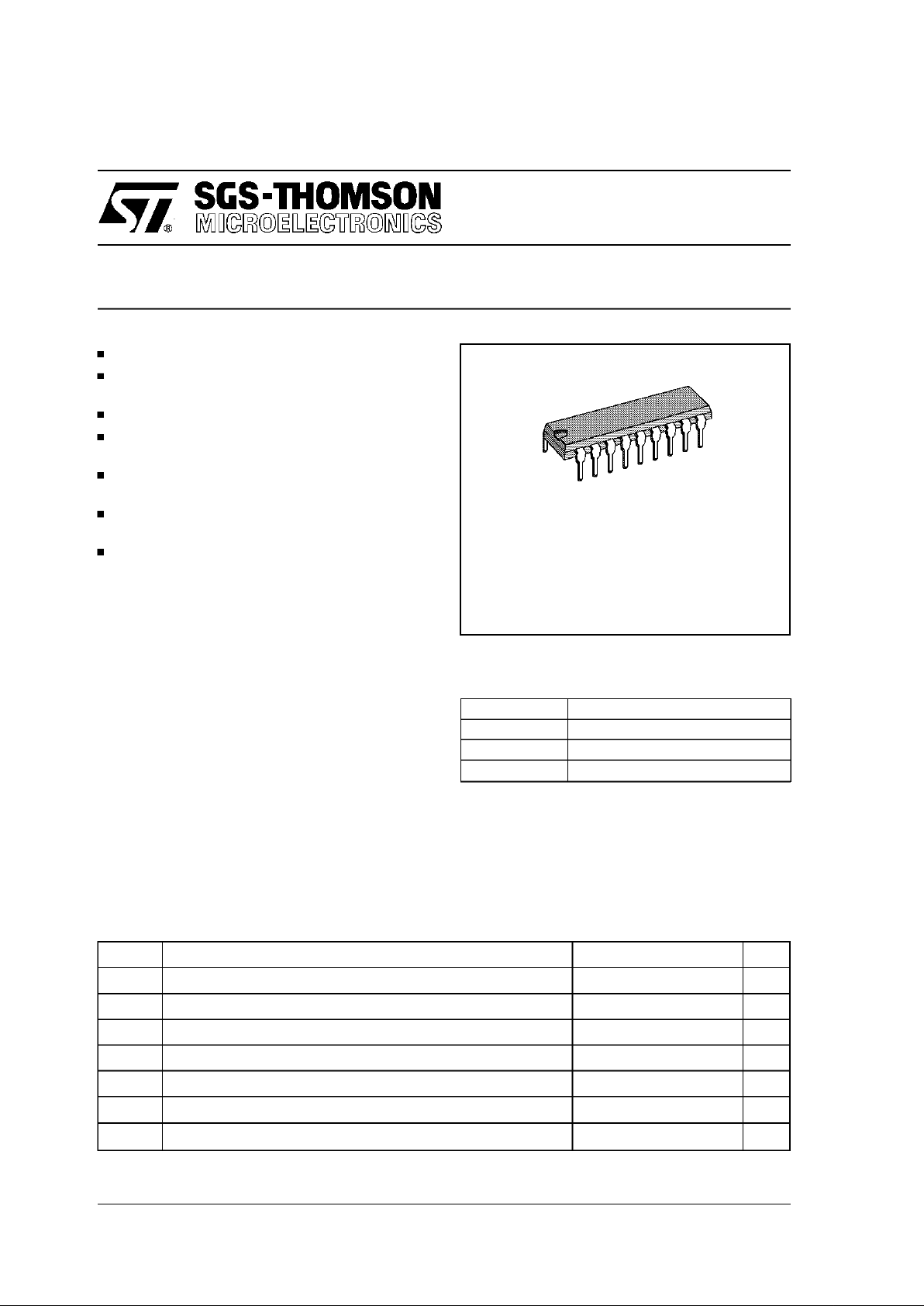
DIP-18
ORDER CODES : L601CL603C
L602CL604C
The four versions interface to all common logic
families:
L601 Generalpurpose
L602 14 - 25 V PMOS
L603 5 V TTL
L604 6 - 15 V CMOS
Theseversatiledevicesareusefulfordrivingawide
range of loads,including solenoids,relays DCmotors, LED displays, filament lamps, thermal printheads and high power buffers.
Symbol Parameter Value Unit
V
CEX
Collector Emitter Voltage (input open) 90 V
I
C
Collector Current 0.4 A
I
C
Collector Peak Current 0.5 A
V
i
Input Voltage (forL602 L603 and L604) 30
I
i
Input Current (for L601 only) 25 mA
P
tot
TotalPower Dissipation a T
amb
=25°C
1.8 W
T
op
Operating Junction Temperature -25 to 150 °C
ABSOLUTE MAXIMUM RATINGS
1/5
2/5
PIN CONNECTION(top view)
L601 L602
L604
SCHEMATIC DIAGRAMS
L603
L601-L602-L603-L604

Symbol Parameter Testconditions Min. Typ. Max. Unit
I
CEX
Output Leakage Current VCE=90V 10 µ
A
V
CE (sat)
Collector Emitter Saturation
Voltage
IC= 300 mA
I
C
= 200 mA
I
C
= 100 mA
I
B
= 500 µA
I
B
= µA
I
B
= 250 µA
2
1.7
1.2
V
V
V
h
FE
DC ForwardCurrent Gain
(L601 only)
VCE=3V IC= 300 mA 1000 -
V
i
Minimum Input Voltage
(ON condition)
VCE=3V
for L602
for L603
for L604
IC= 300 mA
11.5
2.5
5
V
V
V
V
i
Maximum InputVoltage
(OFF condition)
VCE=90V
for L601
for L602
for L603
for L604
I
C
=25µA
0.55
7
0.75
1
V
V
V
V
I
R
Clamp Diode Reverse
Current
VR=90V 50 µA
V
F
Clamp Diode Forward
Voltage
IF= 300 mA 2 2.4 V
t
on
Turn-on Delay 0.5Vito 0.5 V
o
0.4
µs
t
off
Turn-off Delay 0.5Vito 0.5 V
o
0.4 µ
s
ELECTRICAL CHARACTERISTICS (T
amb
=25°C, unlessotherwisespecified)
Symbol Parameter Value Unit
R
th-j-amb
Thermal resistance Junction-ambient Max 70
°C/W
THERMALDATA
3/5
L601-L602-L603-L604

4/5
DIM.
mm inch
MIN. TYP. MAX. MIN. TYP. MAX.
a1 0.254 0.010
B 1.39 1.65 0.055 0.065
b 0.46 0.018
b1 0.25 0.010
D 23.24 0.915
E 8.5 0.335
e 2.54 0.100
e3 20.32 0.800
F 7.1 0.280
I 3.93 0.155
L 3.3 0.130
Z 1.27 1.59 0.050 0.063
DIP18 PACKAGEMECHANICALDATA
L601-L602-L603-L604

Information furnished is believed to be accurateand reliable. However, SGS-THOMSON Microelectronics assumes no responsibility for the
consequences of use of such information nor forany infringement of patents or other rights ofthird parties which may result from its use. No
license is granted by implication or otherwise under any patent or patent rightsof SGS-THOMSONMicroelectronics. Specifications mentioned
in this publication are subject to change without notice. This publication supersedes and replaces all information previously supplied.
SGS-THOMSON Microelectronicsproducts are notauthorized for use ascriticalcomponents in life support devices orsystems without express
written approval of SGS-THOMSON Microelectronics.
1994 SGS-THOMSON Microelectronics - All RightsReserved
SGS-THOMSON Microelectronics GROUP OF COMPANIES
Australia - Brazil- France - Germany- Hong Kong - Italy - Japan - Korea - Malaysia- Malta -Morocco - The Netherlands - Singapore -
Spain - Sweden - Switzerland - Taiwan- Thaliand - United Kingdom - U.S.A.
5/5
L601-L602-L603-L604
 Loading...