

EIGHT DARLINGTONS PER PACKAGE
OUTPUT CURRE NT 400 mA PE R DRIVER (500
mA PEAK)
OUTPUT VOL TAGE 90 V (V
CE (sus))
= 70 V)
INTEGRAL SUPPRESSION DIODES FOR
INDUCTIVE LOADS
OUTPUTS CAN BE PARALLELED FOR
HIGHER CURRENT
TTL / CMOS / PMOS / DTL COMPATIBLE
INPUTS
INPUTS PINNED OPPOSITE OUTPUTS TO
SIMPLIFY LAYOUT
L601-L603
L602-L604
DARLIN GTON AR RA Y S
DIP-18
ORDER CODES : L601C L603C
L602C L604C
The four versions interface to all common logic
families:
DESCRIPTIO N
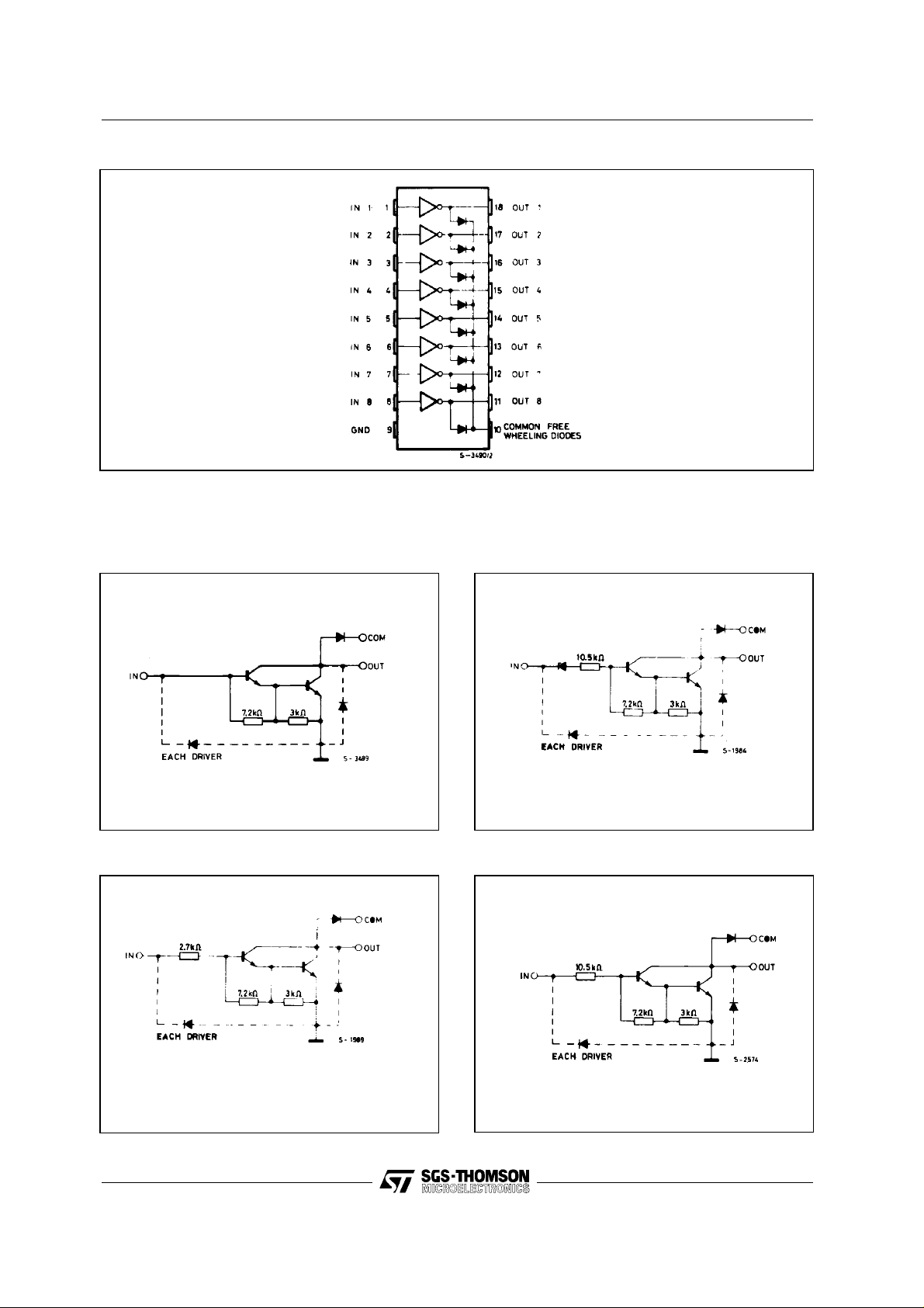
The L601, L602, L603 and L604 are high voltage,
high current darlington arrays each containing
eight open collector darlington pairs with common
L601 General purpose
L602 14 - 25 V PMOS
L603 5 V TTL
L604 6 - 15 V CMOS
emitters. Each channel is rated at 400 mA and can
with stand peak currents of 500 mA. Suppression
diodes are included for inductive load driving and
the inputs are pinned opposite the outputs to simplify board layout.
These versatile devices are useful for driving a wide
range of loads, including solenoids, relays DC motors, LED displays, filament lamps, thermal printheads and high power buffers.
ABSOLUT E MAX IMUM R ATINGS
Symbol Parameter Value Unit
V
P
T
Collector Emitter Voltage (input open) 90 V
CEX
I
Collector Current 0.4 A
C
I
Collector Peak Current 0.5 A
C
V
Input Voltage (for L602 L603 and L604) 30
i
I
Input Current (for L601 only) 25 mA
i
Total Power Dissipation a T
tot
Operating Junction Temperature -25 to 150
op
amb
= 25°C
1.8 W
°C
October 1991
1/5
L601-L602-L603-L604
PIN CONNECTION (top view)
SCHEMATIC DIAGRAMS
L601 L602
L603
L604
2/5

L601-L602-L603-L604
THERMAL DATA
Symbol Parameter Value Unit
R
th-j-amb
Thermal resistance Junction-ambient Max 70
°C/W
ELECTRICAL CHARACTERISTICS (T
= 25 °C, unless otherwise specified)
amb
Symbol Parameter Test conditions Min. Typ. Max. Unit
I
CEX
V
CE (sat)
h
V
Output Leakage Current VCE = 90 V 10
I
Collector Emitter Saturation
Voltage
DC Forward Current Gain
FE
IC = 300 mA
= 200 mA
I
C
I
= 100 mA
C
VCE = 3 V IC = 300 mA 1000
= 500 µA
B
= µA
I
B
I
= 250 µA
B
(L601 only)
V
Minimum Input Voltage
i
(ON condition)
VCE = 3V
for L602
for L603
IC = 300 mA
for L604
V
Maximum Input Voltage
i
(OFF condition)
I
Clamp Diode Reverse
R
Current
Clamp Diode Forward
F
Voltage
VCE = 90 V
for L601
for L602
for L603
for L604
VR = 90 V
IF = 300 mA
= 25 µA
I
C
0.55
7
0.75
1
2
1.7
1.2
11.5
2.5
5
50
2 2.4 V
µA
V
V
V
-
V
V
V
V
V
V
V
µA
t
t
Turn-on Delay 0.5 Vi to 0.5 Vo 0.4
on
Turn-off Delay 0.5 Vi to 0.5 Vo 0.4
off
µs
µs
3/5

L601-L602-L603-L604
DIP18 PACKAGE MECHANICAL DATA
DIM.
MIN. TYP. MAX. MIN. TYP. MAX.
a1 0.254 0.010
B 1.39 1.65 0.055 0.065
b 0.46 0.018
b1 0.25 0.010
D 23.24 0.915
E 8.5 0.335
e 2.54 0.100
e3 20.32 0.800
F 7.1 0.280
I 3.93 0.155
L 3.3 0.130
Z 1.27 1.59 0.050 0.063
mm inch
4/5

L601-L602-L 603- L604
Information furnished is believed to be accurate and reliable. However, SGS-THOMSON Microelectronics assumes no responsibility for the
consequences of use of such information nor for any infringement of patents or other rights of third parties which may result from its use. No
license is granted by implication or otherwise under any patent or patent rights of S GS-THOMSON Mic roelec tronics . Specifications mentioned
in this publication are subject to change without notice. This publication supersedes and replaces all information previously supplied.
SGS-THOMSON Microelectronics pr oducts are not authorized for us e as crit ical components in life s upport devic es or systems wit ho ut express
written approval of SGS-THOMSON Microelectronics.
© 1994 SGS-THOMSON Microelectronics - All Rights Rese rve d
SGS-THOMSON Microelectronics GROUP OF COMPANIES
Australia - Brazil - France - Germany - Hong Kong - Italy - Japan - Korea - Malaysia - Malta - Morocco - The Netherlands - Singapore -
Spain - Sweden - Switzerland - Taiwan - Thaliand - United Kingdom - U.S.A.
5/5
 Loading...