

EIGHT DARLINGTONS PER PACKAGE
OUTPUT CURRE NT 400 mA PE R DRIVER (500
mA PEAK)
OUTPUT VOL TAGE 90 V (V
CE (sus))
= 70 V)
INTEGRAL SUPPRESSION DIODES FOR
INDUCTIVE LOADS
OUTPUTS CAN BE PARALLELED FOR
HIGHER CURRENT
TTL / CMOS / PMOS / DTL COMPATIBLE
INPUTS
INPUTS PINNED OPPOSITE OUTPUTS TO
SIMPLIFY LAYOUT
L601-L603
L602-L604
DARLIN GTON AR RA Y S
DIP-18
ORDER CODES : L601C L603C
L602C L604C
The four versions interface to all common logic
families:
DESCRIPTIO N
The L601, L602, L603 and L604 are high voltage,
high current darlington arrays each containing
eight open collector darlington pairs with common
L601 General purpose
L602 14 - 25 V PMOS
L603 5 V TTL
L604 6 - 15 V CMOS
emitters. Each channel is rated at 400 mA and can
with stand peak currents of 500 mA. Suppression
diodes are included for inductive load driving and
the inputs are pinned opposite the outputs to simplify board layout.
These versatile devices are useful for driving a wide
range of loads, including solenoids, relays DC motors, LED displays, filament lamps, thermal printheads and high power buffers.
ABSOLUT E MAX IMUM R ATINGS
Symbol Parameter Value Unit
V
P
T
Collector Emitter Voltage (input open) 90 V
CEX
I
Collector Current 0.4 A
C
I
Collector Peak Current 0.5 A
C
V
Input Voltage (for L602 L603 and L604) 30
i
I
Input Current (for L601 only) 25 mA
i
Total Power Dissipation a T
tot
Operating Junction Temperature -25 to 150
op
amb
= 25°C
1.8 W
°C
October 1991
1/5
L601-L602-L603-L604
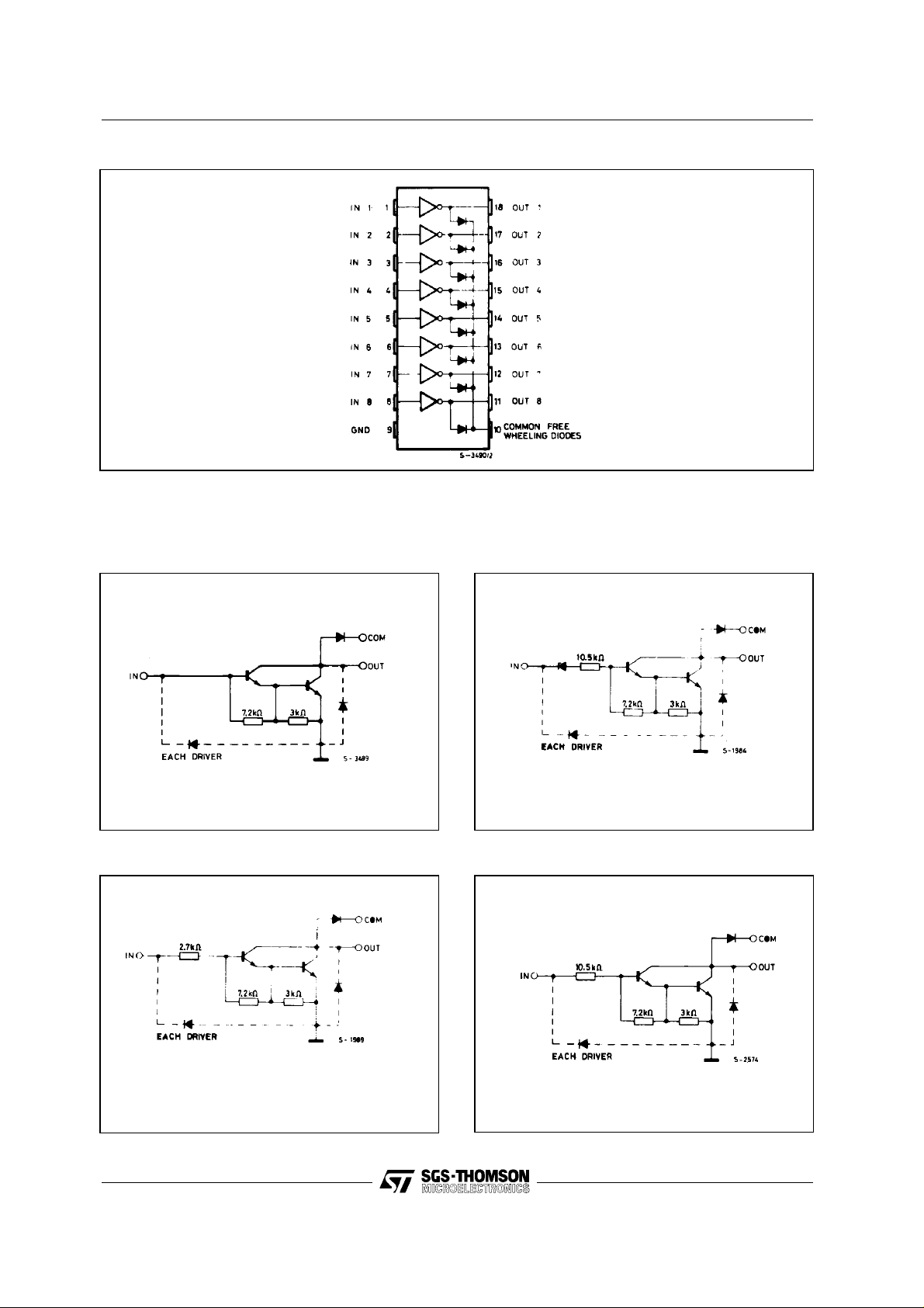
PIN CONNECTION (top view)
SCHEMATIC DIAGRAMS
L601 L602
L603
L604
2/5
 Loading...