

SINGLECHIP READ & WRITE CHA NNEL
SUPPORTS 9-32Mbit/s DATA RATE OPERATION INRLL [1,7] CONSTRAINT
- Data Rate is Programmable
SUPPORTS ZONED BIT RECORDING AP-
PLICATIONS
LOW POWER OPERATION (500mW TYPI-
CAL @ 5V @ 32Mbits/Sec
PROVIDES PROGRAMMABILITY THROUGH
SERIAL MICROPROCESSOR INTERFACE
ANDINTERNALREGISTERS
- Bi-directional access to internal registersof
pulse detector, filter, servo demodulator,
frequencysynthesizerand data separator.
PROGRAMMABLEPOWER DOWN MODES
Fullpower-downmode (5mWmax.)
POWER SUPPLYRANGE 4.3 to 5.5V
DESCRIPTION
The L6000 is a 5V single chip read channel IC. It
contains all the functions needed to implement a
high performance read channel including the
L6000
ADVANCE DATA
TQFP64
(10 x 10)
ORDERING NUMBER: L6000
OPERATING TEMPERATURE: 0°Cto70°C
pulse detector, programmable active filter, servo
demodulator, frequency sinthesizer, and data
separator, at data rates up to 32 Mbit/s. A single
external resistor sets the reference current for the
internalDAC which, in turn, fixes thedata rate.
This device is programmed through a serial port
and banks of internal registers. It is fully compatible with zoned bit recording applications. External componentsdo not need to be changed when
switching between zones. The L6000 is manufacturedusing an advancedBiCMOS technology.
PIN CONNECTION (Top view)
LEVEL R EF V
CLOCK PATH
CLOCK PATH
DATA PATH
FILT NORM OUT
FILT NORM OUT
FILT DIFF OUT
FILT DIFF OUT
FILTER IN
FILTER IN
PTAT R
AGC O UT
SERVO BYP
SERVO REF V
48 47 46 45 44
49
50
51
52
53
54
55
56
57
58
59
60
61
62
63
64
12345
AGC IN
AGC IN
POSITION OUT
DATA BYP
HOLD CAP A
HOLD DATA AGC
DATA TC RES
SERVO TC RES
DAC TP OUT
HOLD CAP B
43 42 41 40 39
678910
PWRDN MODE
VCC CORE DIG
GND PULSE DET
SERIAL DATA I/O
GND CORE DIG
SERVO GATE
38 37 36 35 34
11 12 13 14 15
SERIAL ENABLE
SERIAL CLOCK +
HOLD SRV AGC
REFERENCE FIN
LATCH CAP A
GND FREO SYN
LATCH CAP B
RESET CAP A/B
GND DATA SEP
DS IREFFREQ SYN FLT
33
32LEVEL
DATA SEP FLT
31
DATA SEP FLT
30
VCC DATA SEP
29
READ DATA I/O
28
ADDR MARK DET
27DATA PATH
READ REF CLOCK
26
WRITE CLOCK
25
MULT TP1
24
MULT TP2
23
GND I /O
22VCC PULSE DET
WRITE DATA NR2 IN
21
READ NR 2 OUTPUT
20
WRITE DATA
19
VCC I/O
18
WRITE GATE
17AGC O UT READ GA TE
16
M92L6000-01
FREQ OUT TP
FREQ SYN FLT
VCC FREQ SYN
August 1993
1/24
This isadvanced information on a new product now in development orundergoing evaluation. Details are subject to change without notice.
L6000
Figure1a: Block Diagram (1 of 2)
2/24
Figure1b: BlockDiagram(2 of 2)
L6000
ABSOLUTE MAXIMUMRATINGS
Symbol Parameter Value Unit
Vcc Positive Supply Voltage – 0.5 to 7 V
VoltageApplied to Logic Inputs –0.5 to Vccs + 0.5 V
VoltageApplied to All Other Pins – 0.5 to Vccs +0.5 V
Tstg Storage Temperature – 65 to +150
Tj JunctionTemperature 130
o
o
C
C
3/24
L6000
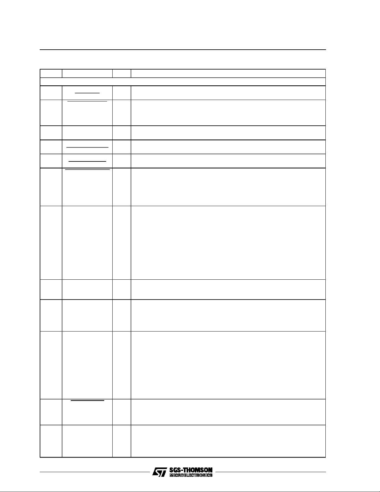
PIN DESCRIPTION
Pin # Symbol Type Description
POWER SUPPLY
30 Vcc DATA SEP - DATA SEPARATOR: PLL analog 5V supply.
14 Vcc FREQ. SYNTH - FREQUENCY SYNTHESIZER: PLL analog 5V supply.
7 Vcc CORE DIG - Internal ECL, CMOS logic digital supply.
19 Vcc I/O TTL BUFFER I/O5V SUPPLY.
59 Vcc PULSE DET - Pulse Detector/Servo Demodulator/Filter analog5V supply.
34 GND DATA SEP - DATA SEPARATOR: PLL analog5V ground.
12 GND FREQ SYN - FREQUENCY SYNTHESIZERl: PLL analog 5Vground.
40 GND CORE DIG - Internal ECL, CMOS logic digital ground.
23 GND I/O - TTL Buffer I/O digital ground.
5 GND PULSE DET - Pulse Detector/Servo Demodulator/Filter analog circuit ground.
INPUT
2, 1 AGC IN,
AGCIN
53, 54 DATA PATH,
DATA PATH
51, 52 CLOCK PATH,
CLOCK PATH
6 PWRDN MODE I PWRDN MODE CONTROL: TTL compatible power control pin. Assertion shuts
4 HOLD DATA AGC I HOLD DATA AGC CONTROL INPUT: TTL compatible power control pin.
38 HOLD SRVAGC I HOLD DATA AGC CONTROL INPUT: TTL compatible control pin.Assertion
47 SERVO REF V I SERVO REFERENCE .VOLTAGE INPUT: This voltage is set to half of the Vcc
37 LATCH CAP A I LATCH CONTROL INPUT: TTL compatible input. Switcheschannel A into
36 LATCH CAP B I LATCH CONTROL INPUT: TTL compatible input. Switcheschannel B into
35 RESET CAP A/B I RESET CONTROL INPUT: TTL compatible input. Enables the discharge of
60, 61 FILTER IN,
FILTER IN
11 REFERENCE FIN I REFERENCE FREQUENCY INPUT: TTL input. Pin REFERENCE FIN has an
22 WRT DATANRZ
IN
17 READ GATE I READ GATE : See clocks and Modes.
26 WRITE CLOCK I WRITE CLOCK: TTL input Write mode clock. Must be synchronous with the
18 WRITE GATE I WRITE GATE: TTLinput. Enables the write mode. See Clocks and Modes.
39 SERVO GATE I SERVO GATE: TTL input. Enables the servo read mode. Active low.
| AGC AMPLIFIER INPUTS: Differential AGC amplifier input pins.
I ANALOG INPUTS FOR DATA PATH: Differentialanalog inputs to data
comparators, full-wave rectifier, and servo demodulator.
I ANALOG INPUTS FOR CLOCK PATH: Differential analog inputsto the clock
comparator.
down all circuitry, except the serialport. Deassertion and the appropriate bit set
in PD register shuts down the selected circuitry. Active low.
Assertion disables the AGC charge pump and holds the input AGC amplifier
gain. Active low.
disables the SERVO charge pump. Active low.
PULSE DET voltage
peak acquisitionmode when low. Cap voltage doesn’t change when high.
peak acquisitionmode when low. Cap voltage doesn’t change when high.
channel A & B hold capacitors when asserted. Active low.
I FILTER SIGNAL INPUTS: Self biased differential input signals to activefilter.
internal pull up resistor. In the test mode, when frequency synthesizer is
bypassed, the REFERENCE FIN frequency requiredis 3 times the data rate.
REFERENCE FIN may be driven by a direct coupled TTL signal.
I WRITE DATA NRZ INPUT. TTL input. Connected to the READ NRZ OUTPUT
pin toform a bidirectional data port. Pin WRT DATA NRZ IN has an internal
pull up resistor.
Write Data NRZ input. For short cable delays, WRITE CLOCK may be
connected directly to pin READ REF CLOCK. For long cable delays,WRITE
CLOCK should be connected to a READ REF CLOCK return line matched to
the NRZ data bus line delay.
4/24
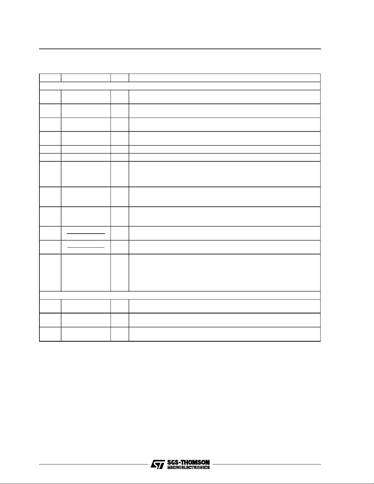
PIN DESCRIPTION(continued)
Pin # Symbol Type Description
OUTPUT
64, 63 AGC OUT,
AGC OUT
29 READ DATA I/O I/O READ DATA I/O: Bi-directional TTL pin. Output is active in the servo mode or
46 POSITION OUT O POSITION ERROR SIGNAL: A Position errorsignal of A minus B output which
56, 55 FILT NORM OUT,
FILT NORM OUT
58, 57 FILT DIFF OUT,
FILT DIFF OUT
28 ADDR MARK DET O ADDRESS MARK DETECT: Tristate output pin with TTL output levels. It is in
25 MULT TP1 O MULTIPLEXED TEST POINTOUTPUT:An open emitterECLoutputtest point.
21 READ NRZ
OUTPUT
27 READ REF CLOCK 0 READ REFERENCE CLOCK: TTL output. A multiplexed clock source used by
24 MULT TP2 O MULTIPLEXED TEST POINT OUTPUT: An open emitter ECL output test point.
20 WRITE DATA O WRITE DATA: TTL output. Encoded write data output. The data is
13 FREQ OUT TP O REFERENCE FREQUENCY OUTPUT: An open emitter ECL output test point.
O AGC AMPLIFIER OUTPUT: DifferentialAGC amplifier output pins.
when both READ GATE andWRITE GATE aredeasserted. In test mode, this
is a TTL input used to drive the data separator. The TTL input is enabled by
setting RDI in the control register CB.
is referenced to SERVO REF V.
O FILTER DIFFERENTIAL NORMAL OUTPUTS: Low pass & boosted filter
output signals.Must be AC coupled to the next stage nominally DATA PATH.
O FILTER DIFFERENTIAL DIFFERENTIADED OUTPUTS: Differentiated filter
outputs should be AC coupled to the next stagenominally CLOCK PATH.
its high impedance state when WRITE GATE is asserted. When READ GATE
is asserted and the register bit is set for soft sector,an address mark search is
initiated in the soft sector operation. This output is latched low (true) when an
address mark hasbeen detected. Deasserting pin READ GATE deasserts pin
ADDR MARK DET.
The testpoint output is enabled by Setting ED inthe control registerCB. The
controllingsignal is PD_TEST in thecontrol register CA. WhenPD_TEST is low ,
thetestpointoutput is the delayed read dataDRD. Theposistive edges of this
signalindicate thedata bit position. The positive edges of theDRD and VCOREF
outputs can be used to estimatewindow centering. The time jitterof DRD’s
positive edge is an indication of media bit jitter.When PD_TESTishigh the test
pointout is the comparator of the pulse qualifier. The positive edge indicatesthat
theinput signal hasexceeded thepositive threshold while a negative edge
indicates that the input signal has gone belowthenegative threshold. Two external
resistors are required to use thispin. Theyshould be removed during normal
operation toreduce power dissipation.
O NRZ OUTPUT DATA: Tristate ouput pin with TTL output levels. It is in its high
impedance state when READ GATE is deasserted. Readdata output when
READ GATE is asserted.
the controller, see Clocksand Modes. During a modechange, no glitchesare
generated and no more than one lost clock pulse will occur. READ REF
CLOCK remains Fout/3 after READ GATE is asserted, until after synchronized
bits are detected.
This test point output is enabled by using the same control bit enabling the
MULT TP1 output. When the controlling signal, PD_TEST is desserted, the test
point output is the VCO reference input (VCOREF) to the phase detector.The
positive edges are phase locked to Delayed Read Data (DRD). The negative
edges of this open emitter output signal indicate the edges of the decode
window. When PD_TEST is high, the test point output represents the state of
the clock comparator in thepulse qualifier. The signal transitions indicate zero
crossing of the differentiated signal from the electronic filter. Two external
resistor are required to use this pin. They should be removed during normal
operation to reduce power dissipation.
automatically resynchronized (independent of the delay between READ REF
CLOCK and WRITE CLOCK) to the reference clock FSout. Falling edge of the
WRITE DATA is the data edge.
The frequency is the frequency synthesizer output frequency. This output is
enabled by control register CA. Two external resistors are required to use this
pin. They should be removed during normal operation to reduce power
dissipation.
L6000
5/24
L6000
PIN DESCRIPTION(continued)
Pin # Symbol Type Description
ANALOG
50 LEVEL REF V O REFERENCE VOLTAGE: Reference voltage output for LEVEL. LEVEL REF V
62 EF IREF I REFERENCE RESISTOR INPUT: An external 1% resistor (RX) is connected
3 DATA BYP – AGC INTEGRATING CAPACITOR: Connected between DATA BYP and Vcc
48 SERVO BYP – AGC INTEGRATING CAPACITOR FOR SERVO: Connected betweenSERVO
45 HOLD CAP A – PEAK HOLDING CAPACITOR A: Tied from this pin to GND PULSE DET.
44 HOLD CAP B – PEAK HOLDING CAPACITOR B: Tied from this pin to GND PULSE DET.
49 LEVEL O HYSTERESIS LEVEL: An NPN emitter output that provides a full-wave
33 DS IREF I REFERENCE RESISTOR INPUT: An external 1% resistor (RR) is connected
42 SERVO TC RES I SERVO TIME CONSTANT RESISTOR INPUT: An external resistor is
15, 16 FREQ SYN FLT,
FREQ SYN FLT
32, 31 DATA SEP FLT,
DATA SEPFLT
41 DAC TP OUT O DAC OUTPUT: A testpoint for some of the on-chip DACs. The output of an
SERIAL PORT
10 SERIAL ENABLE I SERIAL DATA ENABLE: Active high input pin to enablethe serial port CMOS
8 SERIAL DATA I/O I/O SERIAL DATA: Input/Output pin for serial data; 8 instruction/address bits are
9 SERIAL CLOCK+ I SERIAL DATA CLOCK: Positive edgetriggered clock input for the serial data
is derived by referencing VRG (an internal signal) to Vcc PULSE DET.
from this pin to ground to establish a precise reference current for the filter.
PULSE DET. This pin is used when data read mode.
BYP and Vcc PULSE DET. This pin is used whenin servo read mode
rectified signal from LEVEL to LEVEL REF V toset the hysteresis threshold
time constant in conjunction with SERVO TC RES and DATA TC RES. This
level used in VTHRESHOLD DAC.
to this pin to establish a precise internalreference current for the data
separator and Frequency Synthesizer.
connected from this pin to LEVEL to establish the hysteresis threshold time
constant when not in Servo mode.
– PLL FILTER: The two connection points for the frequency synthesizer PLL
differential filter components.
– PLL FILTER: THE Two connectionpoints for the data separatorPLL differential
filter components.
internal DAC is selected bythe values of TDAC1 (MSB) and TDACO (LSB) in
the WS register. The selected DAc output and its corresponding select bits are
as follows: FC_DAC (00), VTH_DAC (0 1), WS_DAC (1 0), andWP_DAC (1
1). When not using the DAC TP OUT pin, the preferred setting is to select the
FC_DAC.
input levels.
sent first followed by 8 data bits. CMOS Input/Output levels.
CMOS input levels. The pin has an internal pull-up resistor.
6/24
L6000
SYSTEM DESCRIPTION
PulseDetector Section
Fast attack/decaymodes for rapid AGC recovery.
Dual rate chargepump for fasttransient recovery.
Low Drift AGC hold circuitry supportsprogrammable gain, non-AGC operation. Temperature compensated,exponential control AGC. Shorted input
switch for transient recovery, during Power down
& Write to read & Idle mode transitions. Wide
Bandwidth, high precision full-wave rectifier. Dual
mode pulse qualification circuitry allows either independent positive and negativethreshold qualification to suppresserror propagation or hysteresis
comparison wich implements alternating polarities. Differential qualifier comparator. TTL READ
DATA I/O signal output available during servo
and idle modes. Timing for shorted inputs and
fast decay functions set internally. 0.5 ns max.
pulse pairing with sine wave input.
Embedded ServoDemodulatorSection
Dual servo burst (A/B) capturewith PositionError
Signal Output. ServoAGCmode which holds sum
of A and B bursts constant. Provision for on-chip
switching of the hysteresis threshold time constant.
Programmable Filter Section
Programmable filter cutoff frequency (fc = 6 to 18
MHz). Programmablepulse slimming equalization
(0 to 9 dB Boost at the filter cutoff frequency).
Matched path timing normal and differential lowpass outputs. Differential filter input and outputs
for noise rejection ±10% cutoff frequency accuracy. ±2% maximum group delay variation in the
passband maintained over the cutoff frequency
tuning range ( fc=6 to 18 MHz ). Total harmonic
distortion less than 1.5 %. No external filter components required. Shorted input switch for transient recovery, during Power down & Write to
Read & Idle mode transitions.
Frequency Synthesizer and Data Separator
Section
1% frequency resolution. Data synchronizer and
1.7 RLL ENDEC. Fast acquisition phase lock loop
with zero phase restart both to data and synthesizer. Fully integrated data separator. No external
delaylines or activedevices required. No external
active PLL components required. Active window
centering symmetry control via serial port. Window shift control ±30%. Includes delayed read
data and VCO clock monitor tests points. Programmablewrite precompensation.Hard and soft
sectoroperation.
THERMAL DATA
Symbol Parameter Value Unit
Rth
R
th j-case
j-amb
Thermal Resistance Junction-Ambient 100 °C/W
Thermal Resistance Junction-Case 20 °C/W
RECOMMENDED OPERATINGCONDITIONS
Vccn SupplyVoltage 4.3 to 5.5 V
T
amb
T
j
Operating Ambient temperature 0 to 70 °C
JunctionTemperature 25 to 125 °C
7/24
L6000
ELECTRICAL CHARACTERISTICS: V
= 5V + 10% - 14%, T
CCn
= 0 to 70 °C, Tj= 25 to 125°C, un-
amb
less otherwisespecified.
Symbol Parameter Test Condition Min. Typ. Max. Unit
POWER SUPPLY CURRENT AND POWER DISSIPATION
Icc Power Supply Current Outputsandtestpoint pins open;
Pd Power Dissipation – 500 660 mW
Tamb= 27°C, 32Mbits/sec
– 100 120 mA
DIGITAL INPUTS AND OUTPUTS
V
IL
V
IH
Low Level Input Voltage – 0.3 0.8 V
High Level Input Voltage 2.0 V
CC
I/O+0.3
I
IL
I
IH
V
OL
V
OH
Low Level Input Current VIL= 0.4V – – 0.4 mA
Low Level Input Current VIH= 2.4V – 100 µA
Low Level Output Voltage IOL= 4.0mA – 0.5 V
High Level Output Voltage IOH= –400µA 2.4 – V
CMOS INPUTS: SERIAL ENABLE, SERIAL DATA AND SERIAL CLOCK
V
IL
V
IH
t
r
t
f
Low level Input Voltage 5V and 25°C – 0.5 V
High Level Input Voltage 4.5 – V
Rise Time 4.3V, 70°C and C = 5pF – 5.0 ns
Fall Time – 4.5 ns
CMOS OUTPUTS: SERIAL DATA I/O
V
OL
V
OH
t
r
t
f
Low Level Output Voltage 5V and 25°C; IOL= 4.07mA – 0.5 V
High Level Output Voltage 5V and 25°C; IOH= +4.83mA 4.5 – V
Rise Time 4.3V, 70°C and C = 15pF – 5.5 ns
Fall Time – 5.0 ns
TEST POINT OUTPUT LEVELS
V
IL
Test Point High Level Output
261Ω to Vcc DATA SEP
Vcc
–V
DATA
SEP-
1.02
– Vcc
V
IH
(MTP1, MTP2, FOUT)
Test Point Low Level Output
402Ω to GND DATA SEP, Vcc
DATA SEP = 5V
261Ω to Vcc DATA SEP
DATA
(MTP1, MTP2, FOUT)
402Ω to GND DATA SEP, Vcc
DATA SEP = 5V
SEP-
1.62
PULSEDETECTOR AND SERVO DEMODULATOR CHARACTERISTICS
V
V
Symbol Parameter Test Condition Min. Typ. Max. Unit
AGC Amplifier Section
The input signals are AC coupled to AGC IN and AGC IN. AGC OUT and AGC OUTare AC coupled to FILTER IN
and FILTER IN.FILT NORM OUT and FILT NORM OUT are AC coupled to DATA PATH and DATA PATH.
IntegratingcapacitorCa = 1000pF is connected between DATABYP andVcc PULSE DET. Unless otherwise specified,
theoutput is measured differentially at AGC OUTand AGC OUT,Fin =4MHz,andthe filter boostat FB = 0dB.
Input range Filter Boost at FC = 0dB
22 – 240 mVpp
(bench testcondition = 2.2 to
18MHz)
Input range Filter Boost at FB = 9dB
14 – 100 mVpp
Fin = FC = 18MHz
(bench test condition = 6 to
18MHz)
DATAPATH/
Voltage AGC IN-AGC IN= 0.1Vpp 0.945 1.05 1.155 Vpp
DATAPATH
Voltage Variation 22mV < AGC IN = AGC IN <
–8.0 – +8.0 %
240mV
Gain Range 1.9 – 22 V/V
8/24

PULSEDETECTOR AND SERVO DEMODULATOR CHARACTERISTICS
Symbol Parameter Test Condition Min. Typ. Max. Unit
Gain Sensititivity with respect to
DATA BYP or SERVO BYPS
pin voltage changes
AGC OUT/
THD AGCOUT - AGCOUT = 0.75Vpp 40 – – dB
AGC OUT
Differential Input Impedance WG = low 4.7 6 8.4 KΩ
Single Ended Input Impedance WG = low
WG = High or when IN Low -Z
mode
VOO Output Offset Voltage Filter not connected – 200 – +200 mV
en Input Noise Voltage AGC OUT, Rs = 0Ω, gain = 22 – 10 15 nV/√Hz
BW Bandwidth gain = 22
AGC OUT/
Single ended output resistance I
= 0 140 180 Ω
O
(1) 50 – – MHz
AGC OUT
PSRR Power Supply Rejection Ratio gain = 22, Fin = 5MHz 45 dB
CMRR Common Mode Rejection Ratio 40 – – dB
Gain Decay Time AGC IN-AGC IN = 240mVpp to
120mVpp,
AGC OUT-AGC OUT = 0.9
Final Value
Gain Attack Time AGC IN-AGC IN = 120mVpp to
240mVpp,
AGC OUT-AGC OUT = 1.1
Final Value
AGC Control Section
The input signal are AC coupled to DATA PATH and DATAPATH, C = 1000pF.
DATAPATH/
Signal Input range (bench test only) – 1 1.5 Vpp
DATAPATH
Id Discharge Current 2.8 4 5.2 µA
Idf Fast Discharge During Fast Decay mode
Current
Ich Charge Pump Attack Current DATA PATH-DATAPATH =
1.15Vpp
Ichf Charge Pump Fast Attack
Current
DATA PATH-DATAPATH =
1.45V
DATA BYP Pin Leakage Current WG = high -0.1 +0.1 µA
LEVELREFV Reference Voltage Vcc
LEVEL REF VOutput Drive -0.75 – 0.75 mA
Duration of shorted input and
(*) –1–µs
Fast Decay modes
Level Output Gain DATA PATH-DATAPATH = 0.5
to 1Vpp
Level Output Bandwidth f
= 11MHz – – 2 dB (2)
IN
Level Offset Voltage Output - LEVEL REF V
(I
=40µA)
L
(*) Guaranted by design.
(1) For correlation automatic test is performed at –3.8dB.
(2) Test limitsunder evaluation.
27 28 dB/V
2.5 3.5
0.65
4.5
0.8
––53µs
––2µs
20xld
–30%
20xld 20xld
+30%
0.126 0.18 0.234 µA
7xlch
–30%
7xlch 7xlch
+30%
– Vcc
PULSE
DET-
2.47
PULSE
DET-
2.0
0.60 0.67 0.75 V/Vpp
–40 – +40 mV
L6000
KΩ
KΩ
µA
µA
V
(2)
9/24

L6000
PULSEDETECTOR AND SERVO DEMODULATOR CHARACTERISTICS (continued)
Symbol Parameter Test Condition Min. Typ. Max. Unit
Data Comparator Section
(The input signals areAC coupled to DATA PATH and DATA PATH)
DATAPATH/
DATA PATH
Kth Threshold Voltage Gain 0.3 ≤ ( LEVEL-LEVEL REF V) ≤
Clocking Section
(The input signals areAC coupled to CLOCK PATH and CLOCK PATH)
Servo Section
RO POSITION OUT Pin Output
(*) Guaranted by design.
(2) Test limitsunder evaluation.
Signal Range – 1 1.5 Vpp
Differential Input resistance 8 – 14 KΩ
Differential Input capacitance – – 5 pF
Comparator Offset Voltage (*) ––±4mV
Threshold Voltage Hysteresis (*) – 20Kth – %
Kth-9% Kth Kth+9% V/V
0.75, Kth = VTHDAC*0.651/127,
38 < VTHDAC < 125,
Vthresh = KTH*(LEVEL-LEVEL
REF V), also, %hyst =
VTHDAC*97.6%/127
Minimum Threshold Voltage LEVEL-LEVEL REF V ≤ 0.1V,
– Vthmin – V
Vthmin = VTHDAC*0.099/127
(*)
CLOCK PATH-CLOCK PATH
– – 1.5 Vpp
Signal Range
Comparator Offset Voltage (*) ––±4mV
Differential Input Resistance 8 – 14 KΩ
Differential Input Capacitance – – 5 pF
Pulse Paring Vs = 1Vpp, F = 4MHz – – 0.5 ns
Prpagation Delay to READ
Vs = 20mVpp sq. wave 4 12 20 ns
DATA I/O
SERVO REF V Voltage Range 2.15V ≤ SERVO REF V ≤ 2.75V 2.15 2.50 2.75 V
SERVO REF V Input Bias
–1 0.2 1 µA
Current
Voltage Gain, SERVO REF V
to POSITION OUT
POSITION OUT Pin Offset
Voltage
POSITION OUT Pin High HOLD CAP A-HOLD CAP B =
Level Output Voltage SERVO REF V = 2.50V,
POSITION OUT Pin Low HOLD CAP A-HOLD CAP B =
Level Output Voltage SERVO REF V = 2.50V Isink =
Resistance
POSITION OUT GAIN (POSITION OUT-SERVO REF
|HOLD CAP A-HOLD CAPB| ≤
0.4V
HOLD CAP A-HOLD CAP B =
0V, SERVO REF V = 2.50V
+1.8V
Isource = 0.5mA
-1.8V
0.5mA
VNG+1.5V ≤ POSITION
OUT ≤ VPG-1.5V
0.98 1.0 1.02 v/v
–0±12 mV
Vcc
PULSE
DET-
1.5
GND
PULSE
DET
+0.3
– Vcc
PULSE
DET-
0.3
– GND
PULSE
DET
+1.5
––50Ω
1.8 V/Vpp
V)/Vpp
HOLD CAP A/B Charge Current Absolute Value 4 – – mA
V
V
(2)
10/24

PULSEDETECTOR AND SERVO DEMODULATOR CHARACTERISTICS (continued)
Symbol Parameter Test Condition Min. Typ. Max. Unit
Id HOLD CAP A/B Disch. Current Absolute value 0.8 1.5 2.2 mA
ILKG HOLD CAP A/B Leakage Cur. – – ±0.5 µA
ILKG SERVO BYP Pin Leakage Cur. HOLDS = Low – – ±0.2 µA
K4 SERVO BYP Pin
450 640 880 µA/Vpp
Charge/Discharge Current
K5 Ibyps = K4 ⋅ [K5 -
DATAPATH
DATAPATH
App
Bpp
]
Maximum SERVO BYP Pin
–
0.70 1.00 1.30 V/V
190 300 490 µA
Charge Current
Tper READ DATA I/O Output Pulse
CL ≤ 15pF 50 – – ns
Period
T1 READ DATA I/O Output Pulse
RDIO ≤ 0.8V 9 23 33 ns
Low Time
Th READ DATA I/O Output Pulse
RDIO ≥ 0.8V 29 – – ns
High Time
Tf READ DATA I/O Output Pulse
CL ≤ 15pF, 2.0V to 0.8V – – 5 ns
Fail Time
Tr READ DATA I/O Output Pulse
CL ≤ 15pF, 0.8V to 2.0V – – 8 ns
Rise Time
PROGRAMMABLE FILTER CHARACTERISTICS
Symbol Parameter Test Condition Min. Typ. Max. Unit
Test Condition s:Vccn = 5V + 10% -14%, T
The input signals are AC coupled to FILTER and FILTER IN. C ≥ 22nF.
FC Filter Cutoff Frequency,
f at -3dB point
FCA Filter fc Accuracy FCDAC = 127 – 10 – +10 %
AN FILTNORM OUTDifferential Gain f = 0.67FC, FBDAC = 0 1.6 2 2.4 V/V
AD FILT DIFF OUT Differential Gain 0.9AN – 1.1AN V/V
FB Frequency Boost @ FC FB (dB) = 20log [0.0273
TGDO Group Delay Variation without
Boost
TGDB Group Delay Variation with
Maximum Boost
VIF Filter Differential Input Dynamic
Range
RIN Filter Diff. Input resistance 5.0 – – KΩ
RIZ Filter Diff. Input Resistance with
Shorted Inputs
CIN Filter Diff. Input Capacitance – – 7 pF
= 0 to 70°C, Tj= 25 to 125°C, unless otherwise specified.
amb
FC = 0.141732MHz *FCDAC,
6 – 18 MHz
42 ≤ FCDAC ≤ 127, FCDAC is
value of frequency DAC
–13–dB
(FBDAC)+1], 0 ≤ FBDAC ≤ 127
FBDAC = 127
@6dB; FBDAC= 36
@13dB; FBDAC = 127
FC = 6MHz to 18MHz,
– 0.75
–2.0
– + 0.75
+2.0
–3 – +3 %
f = 0.2FC to FC FBDAC = 0
FC = 6MHz to 18MHz,
–4 – +4 %
FBDAC = 0, f = FC to 1.75FC
FC = 6 to 18MHz,
–3 – +3 %
f = 0.2 FC to FC, FBDAC = 127
FC = 6MHz to 18MHz,
–4 – +4 %
FBDAC = 127, f = FC to 1.75FC
THD = 1%max, f = 0.67FC,
0.5 – – Vpp
FBDAC = 0
THD = 2%max, f = 0.67FC,
0.75 – – Vpp
FBDAC = 0
Low – Z mode 100 300 500 Ω
L6000
dB
dB
(2)
(2)
(2)
(2)
(2) Test limitsunder evaluation.
11/24

L6000
PROGRAMMABLE FILTER CHARACTERISTICS(continued)
Symbol Parameter Test Condition Min. Typ. Max. Unit
EOUT Output Noise Voltage
Differentiated Output
Output Noise Voltage Normal
Output
Output Noise Voltage
Differentiated Output
Output Noise Voltage Normal
Output
IO- Filter Output SinkCurrent 0.5 – – mA
IO+ Filter Output Source Current 2.0 – – mA
RO Filter Output resistance Single
Ended
Note: FBDAC is value of boost DAC (i.e., no boost)
Filter Control Characteristics (RX = 12KΩ)
VRX Reference Current Set Output
Voltage
FREQUENCYSYNTHESIZERCHARACTERISTICS (RR = 39KΩ)
FIN Input Frequency 8 20 MHz
FOUT Output Frequency – 96 MHz
JFO FOUT jitter TO = 1/FO; Fout = 30MHz – ±400 ps(pk)
M DivideNumber 80 255 –
N Divide Number 25 127 –
TVCO VCO CenterFrequency Period TO = (9.65 + 0.843
VCO Frequency Dynamic
Range
KVCO VCO ControlGain ω =2π/TVCO
KD PhaseDetector Gain KD = 0.7 + 0.43
KVCO x KD Product Accuracy – 28 + 28 %
Reference Clock Characteristics:
Reference Clock Low Time 20 – ns
Reference Clock High Time 20 – ns
DATA SEPARATOR DYNAMIC CHARACTERISTICS AND TIMING (Unless otherwise specified, recommendedoperatingconditionsapply.)
BW = 100MHz, Rs = 50Ω
FC = 18MHz, DACS = 0
BW = 100MHz, Rs = 50Ω
FC = 18MHz, DACS = 127
=27°C
T
amb
(**)
-1
x DR)
FLTR1-FLTR1= 0 (***)
–1.5 ≤ FLTR1-FLTR1 ≤ +1.5,
Fout = 54.0MHz (***)
–1.5 ≤ FLTR1-FLTR1 ≤ +1.5
x DR (***) 0.83KD 1.17KD µA/rad
– 2 7 mVrms
– 1.2 5 mVrms
– 4.6 7 mVrms
– 2 5 mVrms
– – 200 Ω
– 1.5 – V
0.9TO 1.1TO ns
25 ±45 %
0.14ω
o
0.26ωorad/(V-s)
Real Mode
TRRC Read ClockRise Time 0.8V to 2.0V,CL ≤ 15pF – 8 ns
TFRC Read Clock Fall time 2.0V to 0.8V, CL ≤ 15pF – 5 ns
RRC Duty Cycle DR = 32Mbit/s 43 57 %
TNS, TNH NRZ(out) Set Up and Hold Time DR ≤ 20Mbit/s (**) 15.5 – ns
DR >20Mbit/s (**) 13 – ns
TPNRZ NRZ (out) Propagation Delay (**) – ±15 ns
(**) Bench test only.
(***) Preliminarydata.
12/24

DATASEPARATOR DYNAMIC CHARACTERISTICS AND TIMING (Continued)
Symbol Parameter Test Condition Min. Typ. Max. Unit
TAS, TAH AMD Set Up andHold Time (**) 13 – ns
TPAMD AMD Propagation Delay (**) – ±15 ns
TD 1/3 Cell Delay TD = 1/FSOUT,RR = 39KΩ (***) 0.8TD 1.2TD ns
Write Mode
TWD Write Data PulseWidth 1.5V 2TFout/3 2TFout/3 ns
CL ≤ 15pF – 5 + 5
TRWD Write Data Rise Time 0.8V to 2.0V, CL ≤ 15pF – 9 ns
TFWD Write Data Fall Time 2.0V to 0.8V, CL ≤ 15pF – 5 ns
TRWC Write Data Clock Rise Time 0.8V to 2.0V,CL ≤ 15pF – 10 ns
TFWC Write Data Clock Fall Time 2.0V to 0.8V,CL ≤ 15pF – 8 ns
TSNRZ NRZ Set Up Time 5 – ns
THNRZ NRZ Hold Time 5 – ns
TPC Precompensation Time Shift
Magnitude Accuracy
TPCO = 0.04TREF
TPC(max) = 0.28TREF
TPC = nTPCO n=0
– 0.5
+ 0.5
L6000
ns
1 ≤ n ≤ 7
n(0.8TPCO)
– 0.5
n(1.2TPCO)
+0.5
Data Synchronization
TVCO VCO CenterFrequency Period FLTR2-FLTR2 = 0
TO = (8.95 + 0.786 x DR)
-1
0.9TO 1.1TO ns
,
RR = 39kΩ (***)
VCO Frequency Dynamic range –1.5 ≤ FLTR-FLTR2 ≤ +1.5 (***) ±25 ±45 %
KVCO VCO ControlGain
ωo=
2Π
T
VCO
0.14Wo 0.26Wo rad/(Vxs)
–1.5 ≤ FLTR-FLTR2 ≤ +1.5
KD PhaseDetector Gain Read: KD = 0.7 + 0.43
x DR,
0.83KD 1.17KD A/rad
PLL REF = RD 3T Pattern, NonRead: KD = 0.7+ 0.43
x DR,
PLLREF = Fout / 2 (***)
KVCO x KD Product Accuracy – 28 + 28 %
VCO PhaseRestart Error – 4 ns
Decode Window Cent. Accuracy – ±1.5 ns
Decode Window Width 2TORC/3
–ns
- 1.5
SERIALPORT TIMING
Symbol Parameter Test Condition Min. Typ. Max. Unit
Tc SERIAL CLOCK+ Data Clock Period 100 – ns
Tck1 SERIAL CLOCK+ Low Time 40 – ns
TcKh SERIAL CLOCK+ High Time 40 – ns
Tsens Enable to Clock Delay Time 35 – ns
Tsenh Clock toDisable Delay Time Delay from SERIAL
CLOCK+ falling edge
Tds Data Setup Time 15 – ns
Tdh Data Hold Time 15 – ns
Tdskewl Clock toValid DataDelay Time Delay from SERIAL
CLOCK+ falling edge
Tdskewe End of Valid Data to Clock – 0 ns
Tsendl Time toTri-stated SERIAL DATA I/O Delay from falling edge
of SERIAL ENABLE
Tturnd SERIAL DATA I/O Turnaround Time 70 – ns
Tsl SERIAL ENABLE Low Time 200 – ns
(**) Bench test only. (***) Preliminary data.
100 – ns
–27ns
–50ns
ns
13/24

L6000
MODECONTROL
READ GATE
WRITE GATE
SERVO GATE
PWRDN MODE
PWRDN Mode
Register bits
PD
SD
FLT
DS
DESCRIPTION
FS
X X X O X X X X X FULL POWER DOWN MODE :Only the serial interface
0 1 1 1 0 0 0 0 0 READ MODE : The entire FRONT END is turned on, the
1 0 1 1 0 0 0 0 0 WRITE MODE : The FRONT END is inactive. The assertion
0 0 1 1 0 0 0 0 0 IDLE MODE : Allthe front end circuitry is active andoperating.
0 X 0 1 0 0 0 0 0 SERVO MODE 1 : The Pulse Detector and Servo
0 X 0 1 0 0 0 1 1 SERVO MODE2 : This mode has both the Frequency
remains operational. Switching from this mode to either
Servo, Read or Idle modes initiates certain Read Channel
states. Switchingdirect to Write modes is an illegalsequence.
See Circuit Opertion.
READ DATA I/O pin isinactive, and the AGC amplifier is
active, with unshorted inputs ( low-impedance mode off ) and
in tracking mode. The HOLD DATA AGC inputis enabled.
The Data Separator section initiates its Address Mark search
on the assertion of READ GATE. It then starts its phase lock
up sequence after Address Mark detection occurs. After
3 ⋅ 3T following the Address Mark Detect ion the DS PLL
is switched from Fout/2 to DRD and the look-in sequence is
initiated. After 19 ⋅ 3T RRC switche from Fout/3 to DATA
SYNCHRONIZER Vco/3and NRZOUT is enabled. After.
Read mode is maintained until the deassertion of READ
GATE.
of WRITE GATE causes the pin WRT DATA NRZ IN to
become an active input, and the pins READ NRZ OUTPUT
and ADDR MARK DET are floated. The inputs of both the
Active filter and AGC amplifier are shorted ( i.e. the low-
impedance state entered ). The PLL is locked to the
Frequency Synthesizer divided by 30. n WRITE GATE
assertion, two address marks ( each 7 0’s, 1, 7 0’s, 1, 11 0’s,
1, 11 0’s ) are generated and than thepreamble of three 3T
groups. WRT DATA NRZ IN must be zero until these patterns
have been output from WRITE DATA. Write Mode is ended
when Write Gate is deasserted. This starts the AGC Amplifier
fast attack/decay currents acquisition, as well as unshorting
the filterand AGC Amplifierinputs.
The Data Separator VCO is phase locked to Fout. TheREAD
REF CLOCK outputs is theFrequency Synthesizer divided by
3. The pin READ NRZ OUTPUT is floated, ADDR MARK DET
is high, READ DATA I/O is an active output of the pulses
detected and HOLD DATA AGC is enabled. The inputs to the
AGC Amplifier and filter are unshorted.
Demodulator circuitry is operating, and the HOLD DATA AGC
input is disabled. The Data Separator is on andit is phase
locked to the Frequency Sinthesizerwhich is also on. Thepin
READ DATA I/O is an active output.
Synthesizer and Data Separator major blocks powered down,
otherwise it is the same as SERVO MODE 1 . This mode is
intended to reduce power dissipation when the systhem is
just track following. Since only the Pulse Detector and Active
Filter are powered on, this is also known as FRONT END
TEST MODE.
14/24

MODECONTROL(continued)
PWRDN Mode
PD
READ GATE
WRITE GATE
SERVO GATE
PWRDN MODE
Register bits
SD
FLT
DS
L6000
DESCRIPTION
FS
X X X 1 1 1 0 1 1 TEST FILTER MODE : All major blocks except the Active
0 1 1 1 1 1 1 0 0 TEST DATA SEPARATOR READ MODE : Only the Data
1 0 1 1 1 1 1 0 0 TEST DATA SEPARATOR WRITE MODE : Onlythe Data
X X X 1 1 1 1 0 0 TEST FREQUENCY SYNTHESIZER MODE: The front end is
CIRCUITOPERATION
General
The L6000 is a state of the art integrated read
channel.The majorfunctionalblocks are :
1) Pulse Detector and Servo Demodulator,with
dual servo burst measurement channels and
2 differentqualificationschemes for data.
2) Tunable Active equiripple filter with tunable
Filter with Boost and Differentiator are powered down via
Register ( R02 ).
Separator and Frequency Synthesizer are on, and the pin
READ DATA I/O is a test input.
Separator Write circuitry and the Frequency Synthesizerare
on, for testing this specific circuitry.
powered down. The Frequency Synthesizer is powered on for
testing.
(R02). The following table defines the power
down modes and register bits controlling them:
Bit Symbol Function
0
1
2
3
4
5-7
PD
SD
FLTR
DS
FS
Pulse Detector Power Down
Servo Demodulator Power Down
FilterPower down
Data Separator Power Down
Frequency Synthesizer Power Down
Bits 5-7 are Hard-Coded to 111.
Pulse slimming Boost and Active Differentiator.
3) (1, 7) RLL Combined Data Separator and
ENDEC with active window centering and
marginshifting fromexternalcommands.
4) A (M+1) divide by (N+1) Frequency synthesizer, using an external reference, and with 7
bitsof DAC control accuracy.
5) A high speed serial interface controllingmost
functionsand adjustement.
The L6000 is designed to be usedwith data rates
as high as 32 Mbits/sec. Selection of a different
When the PWRDN MODE pin is asserted it powers down ALL functions with the exception of the
serial port, which remains active in ALL power
down modes. When the PWRDN MODE pin is
deasserted, each individual major function block
can be powered on or OFF separately from the
serial port PD register. This feature is useful for
sophisticated power saving state machines in
systems. Toggling the bit in the register is the
only necessarycondition to turn on or OFF a major block; PWRDN MODE doesnot have to be cycledfor each separate registerload.
recording density is done by setting new divisors
in the FrequencySynthesizer via serial registers.
Serial Interface
The serial interface consists of the 3 signals SE-
Power Management
The serial interface should load all appropriate
control registers as soon as Power on Reset
clears in the system. This prevents spurious conditions in all the affected blocks. After the registers are written, then the appropriate Power down
modes can be used. The power management of
the L6000 is under the control of the PWRDN
MODE pin and the Power Down Control Register
RIAL ENABLE, SERIAL CLOCK and SERIAL
DATA I/O. The first two signals are inputs which
are always powered on and active. SERIAL
DATA I/Ois a bidirectionalpin which becomes an
ouput on a register read. A value can be put into
the L6000 (register WRITE) or a value can be interrogated from the L6000 (register READ). The
bottom half of the diagram is a register READ
where a value is interrogated from the L6000. To
do either operation, SERIAL DATA ENABLE is
15/24

L6000
The internal registermap for the serial port is shownbelow:
5
0
0
0
0
0
0
0
0
0
0
0
0
Blk Diagr.
Address
6
0
0
0
0
0
0
0
0
0
0
0
0
R02
R03
R0B
R0A
R12
R1A
R06
R0E
R04
R05
R0D
R0C
Symbol Function
PD
FCutoff
FBoost
DVTH
SVTH
CA
PSNN
PSMM
VCO CENT
WIN SHIFT
WRT PREC
CB
Power Down Mode Control
DACF-Filter cutoff Frequency Control
DACS-Filter Boost Control
Pulse Detector Voltage Threshold Control (Data Read Mode)
Pulse Detector Voltage Threshold Control (Servo Read Mode)
Control A (PulseDetector, Filter, frequency synthesizerControl)
Counter Value (frequency synthesizer)
Counter Value (frequency synthesizer)
VCO CenterFrequency
Window Shift Magnitude,Direction
Write Precomp magnitude
Control B (Data Separator, EndecControl)
Address Bits
LSB MSB
4
3
2
1
0
1
0
1
1
1
1
1
0
1
0
1
0
1
0
1
0
0
0
0
1
0
1
0
0
0
0
0
0
0
0
0
1
0
0
1
0
1
0
0
1
1
0
0
0
1
0
1
1
0
0
1
0
0
1
0
1
1
0
1
1
The bit map of each register (except CA, CB& PD) is as follows:
FCutoff register
FBoost register
DVTH register
SVTH register
PSN register
PSM register
VCO CENT register
WIN SHIFT register
WRT PREC register
where: X = Unused bit or don’tcare bit
X
X
DEDC
SEDC
X
M7
FSC
TDAC1
X
DEDC = Enable dual comparator qualifier in Data read mode.
SEDC = Enable dual comparator qualifier in Servo read mode.
FSC = The frequency synthesizer back comparator state
TDAC1 = DAC Testing control bit #1
TDAC0 = DAC Testing control bit #0
FC6
FB6
VD6
VS6
N6
M6
DR6
TDAC0
X
FC5
FB5
VD5
VS5
N5
M5
DR5
WSE
X
FC4
FB4
VD4
VS4
N4
M4
DR4
WSD
X
FC3
FB3
VD3
VS3
N3
M3
DR3
WS3
WP3
FC2
FB2
VD2
VS2
N2
M2
DR2
WS2
WP2
FC1
FB1
VD1
VS1
N1
M1
DR1
WS1
WP1
FC0
FB0
VD0
VS0
N0
M0
DR0
WS0
WP0
Control register CA: Control register CB:
Bit Symbol Function Bit Symbol Function
0 EPDT Enable Phase Detector (frequency
synthesizer)
1 UT Pump Up (FLTR1 sources current,
FLTR1 sinks current) Test mode
2 DT Pump Down (FLTR1 sinks current,
FLTR1 sources current) Test Mode
3 ET Enable frequency synthesizer Circuit
Function
4 BYPT Bypass frequency synthesizer Circuit
Function
5 PD TEST Enable Pulse Detector Test
Points,COUT and DOUT
6 FDCT ForceAGC Charge Pump into Fast
Decay Mode
7 Unused 7 SOFT Select Soft or Hard Sector Operation
asserted, then the SERIAL CLOCK+ is driven
with the positive edge latching the state of SERIAL DATA. The actual data is latched into each
register in the L6000 when SERIAL ENABLE is
disasserted, so this signal MUST be driven low
16/24
0 DW Direct Write (Bypass Endec)
1 GS Enable Phase Detector Gain
Switching
2 READDATAI/O Pin Input Control
3 EPDD Enable Phase Detector (Data
Separator)
4 UD Pump Up (FLTR2 sources current,
FLTR2sinks current) Test mode
5 DD Pump Down (FLTR sinks current,
FLTR2sources current) Test mode
6 ED Enable Data SeparatorTest Point
Outputs
after EACH register write; failure to deassert SERIAL ENABLE before a 17th SERIAL CLOCK+
will erase ( invalidate ) the previous 16 clock cycles. This also precludes SERIAL CLOCK+ from
being a free running clock in the system. The

L6000
WRITE operation format is the following. The first
bit is LOW, meaning write, followed by the 7bit
register address, LSB first. The last 8 bits then
are the data to be written to the register,also LSB
first. During this to entire operation, SERIAL
DATA I/O is an active input. The READ operation
format is the following. The first bit now is HIGH,
meaning read, and that is followed by the 7bit
register address, LSB first. Upon receipt of the
last bit of address, the pin SERIAL DATA I/O
turns and becomes an active output, and outputs
the 8 bits stored in the addressed register, LSB
first on the following8 SERIAL CLOCK+s.
PulseDetector and Servo Demodulator
The purpose of the Pulse Detector is to qualify
and detect the position of flux transitions written
on the disk. The first stage of the Pulse Detector
is the AGC amplifier. It is a wideband, differential
amplifierwhich characteristic(Gainvs. Voltage) is
positive slope and linear in DB and thermal compensated.The amplifier inputs have a low-impedance state where the inputs are shorted by a FET
switchduring modes where transientsare likely to
occur. The amplifier gain is controlled by 2 capacitors connected to to the DATA BYP and
SERVO BYP pins. The capacitor which controls
the gain is selected by the SERVO GATE signal,
asserted meaning Servo. In modes where the
AGCis powered on, the selected capacitorwill be
charged from a dual rate charge pump. When the
individual signals HOLD DATA AGC and HOLD
SERVOAGC are asserted,the respective capacitors are disconnectedfrom the charge pumps, but
they remain in control of the AGC gain. If a fixed
gain is desired, a voltage divider can be connected to either DATA BYP or SERVO BYP pin.
In order to minimize the time required to restore
the correct AGC output amplitude, the input
switching to unshorted inputs and the AGC attack/delaycurrents are under timed, state control.
The time to restore the inputs and AGC to normal
operation is set to 1 usec. However, the AGCattack is controlled by amplitude and may take
longer to settle. The nominal AGC attack (discharge)current is set to 0.18 mA but is increased
to 1.3 mA when the AGC amplitude exceedes
1.25 times its set point. The nominal AGC decay
current is increased from 0.004 mA to 0.080 mA
in the recovery fast/decay mode. The high decay
current of 80uA is only on for the second microsecond after the mode switch initiates the AGC
reacquisition. Note that the fast Decay current is
available in the recovery mode, while any amplitude transient over the threshold will activate the
fastAttack current.
The modes where the inputs go from shorted to
unshortedare :
1) From Full Power Down either Servo mode
(SERVOGATE active)
2) From Full Power Down to Idle mode.
3) From Full Power Down toRead mode.
4) From Write to Read mode.
5) From Write to Idlemode.
The modes where the inputs go from unshorted
to shorted are : 1) From Read to Write mode. 2)
Fromany mode to Full Power Down mode.
The modes where the fast attack and decay currentsbecome active are :
1) From Full Power Down to Idle mode.
2) From Full Power Down toRead mode.
3) From Write to Read mode.
Nominally the AGC amplifier outputs will be AC
coupled to the Active Filter outputs and then the
Active Filter outputs, both Normal and Differential
will be AC coupled back to the Pulse Detector
block.
Pulse Detector
This block has 4 inputs, 2 fully differential pairs.
The CLOCK PATH inputs are a zero crossing detector, zero crossing assumed to occur at the amplitude peaks of the pulses. This input pairs shall
be connected to the Active Filter differentiator.
The DATA PATHinputs are amplitude ( threshold
) qualifiers and are to be connectedto the Active
Filter normal outputs. Call factory for schematic
for the recommended connection in the system.
Dual threshold comparators are available in the
Pulse Detector. If the DEDC bit is set in the
DataVth register ( ROA ), then separate comparisons are done on negative and positive peaks. If
the bit is reset, then the polarity of the next pulse
to be qualified must be opposite of the last. This
check can lead to a 2 bit missing error for just 1
pulse under threshold. The threshold used for
comparison is set in the two threshold register
DataVth and ServoVth. These register feed the
threshold DAC (VTHDAC) which developes the
actual floating hysteresis level and thresholds
from the input LEVEL (a bufferred signal rectified
from the filter normal outputs. The hysteresis is
always a percentage, of 0.7 the peak to peak
swingat DATA PATH inputs, and is accurate from
10 to 80 % with a 1 % accuracy. The floating hysteresis generator also has a time constant which
is developed from the components connected to
SERVO TC RES, DATA TC RES, LEVEL, and
LEVEL REF V. This time constant is, in effect, a
time domain filter implemented in the qualifier
channel that has the purpose to realize an envelope detector on the rectified signal feeding the
DATA PATH inputs. The two constant is changed
depending on SERVO GATE state.. Recommended values for Rext on SERVO TC RES and
DATA TC RES is TBD ; for Cext on LEVEL and
LEVEL REF V it is TBD. The output of the Pulse
Detector block is READ DATA I/O, and this pin is
activeONLY in the Idle and Servo modes. It is an
approximately 24 nsec negative going TTL com-
17/24

L6000
patible data pulse. The PD- Test bit of theregister
CA controls this output being active. NORMAL
operation is for this bit to be reset, but for testing
the Data Separatoras an input,it should be set.
ServoDemodulator
When in Servo mode all circuitry not needed to
acquire embedded servo position information is
deactivated, the AGC loop is switched to the
servo BYP capacitor, the READ DATA I/O output
is activated, the SERVOTC RES Servo time constant setting resistoris connected to LEVEL REF
V, and the hysteresis threshold level is set to the
Servo threshold. Three servo control inputs,
LATCH CAP A, LATCHCAP B, and RESETCAP
A/B control the servo peak sample and hold
functions. When HOLD SERVO AGC is deasserted, the servo charge pump drives the SERVO
BYP hold capacitor. The current magnitude and
direction is determinedby the formula :
Ibyp2 = gm1*( Vset-Va ( DIN ) pp-Vb ( DIN ) pp )
where : gm1 = 640 uA/Vpp
Vset= 1.0Vpp
Va/b( DIN ) pp = peak to peak A or B servo pattern signal voltages across DATA PATH and
DATAPATH.
When SERVO GATE is deasserted, there is an
automatic 1 usec break before make switch in an
action before the capacitor on the DATA BYP pin
is reconnected to the AGC gain control.
The POSITION OUT pin outputs a voltage equal
to the difference beetwen HOLD CAP A and
HOLDCAP B referenced to SERVOREF V.
The DATA BYP and SERVO BYP capacitor voltages will be held constant(subject toleakagecurrent) during sleep mode, when the respective
HOLD DATA AGC and HOLD SRV AGC signals
are low, and when they are not being used to
controlthe AGCloop.
Test bits and modes
The FDCT bit in the Control A register forces the
Charge pump into the fast decay (or 0.08 mA current) mode. This bit should be set during power
up in a normal system. The PD_Test bit stands
for Pulse Detector Test and should be reset, so
that MULT TP1 outputs Delayed Read Data
(DRD), and MULT TP2 outputs the Data Separator VCO(divided by two).
Programmable Active Filter
The outputs of the AGC Amplifierof the PulseDetector block are normally AC coupled to inputs of
the Active Filter. The low-pass portion of the active filter is to bandlimit noise. The FCutoff register is used to set the cutoff frequency of this portion. The filter type is a 7 pole 0.05 degree
equiripple linear phase error low-pass. Shaping
response may also be introduced, via the boost
equalizationavailable. This is done to account for
deficienciesin the recordingprocess. The FBoost
register sets the amount and polarity of boosting
the cutoff frequency in the Active Filter. The
amount set is contained in the FB register. The
boost is accomplished by a two pole high-pass
feed forward section in parallel with the low-pass
filter. A differentiatoris also part of the Active Filter major block to turn the recovered peaks into
zero crossing. The differentiator is a single pole,
singlezero active type. The Active Filter blockhas
2 outputs. One set is the differentialoutputs from
the low-pass/equalizationportion. The other set is
the differential outputs of differentiator portion.
Both sets of the outputs have matched delays to
maintain timing integrity when re-entering the
PulseDetector major block. The currentreference
for the FC and FB DAC is developedoff of the EF
IREF input. The recommended value of the resistor at EFIREF is : 12 Kohm ±1% .
Thenormalizedlow-pass transfer functionis :
(i.e. ω
Vnorm
=2πfc = 1) are: (see Fig. 2 forreference)
c
2
+ 0.75928)
D(s)
⋅ AN
Vi
(1−Ks
=
Thenormalized differentiator transfer function is :
Vdiff
=
Vi
whereD(s) = (1 + s + 1.27936 +s20.75928)⋅
(1 + s 0.52247 + s
(1−Ks
2
+ 0.75928) ⋅ s ⋅ 1.16099
s)
D (
2
0.33882) ⋅ (1 +s 0.21323 + s
⋅ AD
0.1862)⋅ (1 + s 1.16099)
AN and AD are adjusted for a gain of 2 at fs =
(2/3)FC.
FrequencySynthesizer
The Frequency Synthesizer block is used to develop source recording frequencies for writing
data in the system. It is Phase Lock Loop based
circuitwith divide countersset by registersloaded
from the serial interface. The frequency generated, Fout, is 3 times the HOST data rate in
Mbits/sec, and is 2 times the CODE data rate of
pulses written on the disks. The resolution of the
frequency is 1%. The filter to the PLL is external,
and fully differential on the pins FREQ SYN FLT
and FREQ SYN FLT. A second order filter is recommended.The Fout frequency is used in Read,
Write and Idle modes as the reference for the
DataSeparator PLL. If the ET bit of ControlA register is set in these modes the FRE OUT TP pin
will output the Synthesizerclock Fout. Setting this
bit in Read mode is not recommendedin order to
reduce jitter and decrease power dissipation. To
set the frequency, the input REFERENCE FIN is
fed to the divide by N+1 counter, and this counter
output is the reference input of the Frequency
2
18/24

Figure2: Normalizedblockdiagram for filter
L6000
Normalizedfor ω
and ADare adjustedfor a gain of 2 @ f = 0.67fc
A
N
=2Πfc=1
c
to denormalized the frequency it isnecessaryto substitudes with
Synthesizer phase comparator. The Frequency
SynthesizerVCO is fed to divide by M+1 counter,
and the counter output is the other phase comparator input.
Thisdevelops the frequency:
1,performs write precompensation,generatesthe
preamble field and inserts address marks as requested.
The data rate used for recovery is determined by
the VCO Center Frequency DAC, otherwise
called the PLL Control DAC and the external re-
(M + 1
Fout =
Note : For the new value in the M and N registers to be transferred
totheirrespective counters,theVCO CenterFrequencyDAC register
must beloaded withits value.This means thenormalorder ofregister
writes tochange the FrequencySynthesizer outputfrequency would
be:
1) Write M and/orN register with its ( their ) new value ( s ).
2) Write the VCO CenterFrequency register with its new value.
(N+ 1)
)
FREF
TheRREF is choosen to set the frequencyrange
of both the FDSVCOand theDSVCO.
sistor RREF connected to the pin DS IREF and
Data Separator GND. The differential filter connected to the pins DATA SEP FLT and DATA
SEP FLT determinethe loop gain, bandwidthand
damping.A second order filter is recommended in
most systems, and the filter will determine the
system characteristics. The phase comparator of
the Data Separator PLL utilizes phase only comparisons when locked to the disk data stream,
only making a phase comparison when a data bit
is available. In the frequencycomparisonmode, a
phase compare is is done to every VCO transi-
CLOCKSAND MODES
tion. Thislatter isdone wheneverthe PLL is powered on and data is NOT being read from the
WRITE
GATE
Notes: 1 Until the VCO locks to the new source,the VCO/2 entries
will be FREQ OUT TP/2.
2: Until theVCO locks to the new source, the VCO/3 entries will be
FREQ OUT TP/3
3: WRITE GATE = READ GATE = 1 is undefinedand illegal
READ
GATE
O
O
1
VCO
Fout/2
0
DRD
1
Fout/2
0
REF
RRC
Fout/3
VCO/3
Fout/3
DECCLK ENCCLK MODE
Fout/2
VCO/2
Fout/2
Fout/2
Fout/2
Fout/2
IDLE
READ
WRITE
disk. By acquiring both phase and frequencylock
to the input reference frequency and utilizing a
zero phase restart technique, VCO transients are
minimized and false lock to READ DATAis eliminated. The two control inputs READ GATE and
WRITE GATE directly switch the operations of
the Data Separator. In addition, there are two further submodes split between the Hard Sector
mode of operation and the Soft Sector.Hard Sector operation is selectedby resetting the SOFT bit
control B register via the serial interface. The as-
DataSeparator
The data separator circuit is a complete 1.7 RLL
ENDEC data recovery circuit. In the read mode,
the circuit performs data synchronization, sync
field search and detect, address mark detect,
Read-back clock generation and data decoding.
In the write mode, the circuit converts NRZ data
into the ( 1.7 ) RLL format describedin the Table
sertion of READ GATE causes the Data Separator to enter the lock up sequence, and Read
mode. Read mode continues until READ GATE
deassertion. The assertion of WRITE GATE
causes the Separator to enter Write mode.
WRITE GATE should not be deasserted until the
last bit is written on the disk. Assertion of BOTH
signals at once is illegal and will lead to unpredictableresults.
s
2Π fc
19/24

L6000
1.7 RLL ENCODING
Previuos RLL
Code Word
Last Bits
X
X
X
X
1
1
0
0
X
X
X
X
Y2’
0
0
0
0
0
0
0
0
1
1
1
1
Y3
NRZ Data Bits
Present Next
0
0
1
1
1
1
0
0
0
0
0
0
0
0
D1
X = Do Not Care
* = Not All Zeros
1, 7 RLL CODE SET
0
1
1
0
0
1
1
0
0
1
1
D2
1
0
*
0
1
0
1
0
1
0
*
D3
X
X
0
*
X
X
X
X
X
X
0
*
D4
RLL
Code Bits
0
1
1
1
1
0
0
1
0
0
0
0
0
0
0
0
0
0
1
0
1
0
0
0
Y2
Y1
1
0
0
0
1
0
1
0
1
0
0
0
Y3
ReadMode
The phase comparator enters its phase only compare mode after three cycles of a 3T pattern.This
means that the leading edge of READ DATA
arms the comparator and then the phase comparison is done between the trailing edge of
READ DATA and the rising edge of the closest
VCO cycle. The time between the two READ
DATA edges is 1 VCO cycle, or 1/3 bit cell and is
generated by an internal one-shot and the PLL
ControlDAC.
The Window Shift function of the L6000 is provided for testing purposes, and advanced recovery from read errors. To shift the bit position from
its nominal centerd position in the decode window, a value is written to the WinShiftregister via
the serial interface. The shift value will take effect
after SERIAL ENABLE is deasserted. The direction is determined by the Directionbit in the register. See the Register Definition section for the
complete set of values and their effect. To do the
Windowshift function, the WinShiftregister sets a
current in the WS DAC wich than adds or subtracts current in the 1/2 VCO cycle delay for the
Data Synchronizer. This then changes the position of the trailing edge of the READ DATA pulse
at the Synchronizer ONLY. Since the edge position doesn’t change relative to the VCO at the
phase lock is unaffected,and only the bit position
is moved inside the decode window in the Synchronizer.
The VCO has a zero phase restart feature which
allows for very quick acquisition of the READ
DATA phase being recovered from the disk. The
VCO is kept at frequencyFout during Idle mode,
and when Preamble is detected, the zero phase
restart first turn OFF the VCO, then restarts it in
phasewith the first received databit.
ABOVEVOLTAGE MONITOR
The above voltage bit is used to actively center
the bit in the window by trimming the operating
current of PLL Control DAC to its midpoint of operation.
To optimize this time from temperatureand process variations, the Above Voltage check should
be performed on a periodic (at least every frequency switch) basis. This will center the operating point of the VCO and set the 1/2 VCO cycle
delaycloset to nominal.
AboveVoltage monitor bit (Register4, B7):
This feature allows the drive microprocessor to
set the VCO to the center of its capture range,
and to remove any offset error from the delay
one-shots in the DataSeparator. By changingthe
setting of the VCO center register (04), the drive
microprocessor caN maxime the loop lock range
(and minimize margin timing error at power up).
The comparator driving this bit allows for setting
the VCO DAC (Register 04) to place the Data
Separator VFO to its mid-point of operation. It is
intended for use a power-up time calibration, but
can be done at any time power is applied to the
L6000.The microprocessor which loadsthe register values monitors this bit in the following algorithm:
1.Set the Numerator and Denominator values
for the first data rate in Register 0E and 06,
respectively.
2. Write the nominal value chosen to the VCO,
DAC, Register 04.
3.Read the Above Voltage bit: if it is HIGH, decrease the value in Register 04 by 1. If it is
LOW, increasethe value in Register04 by 1.
4.Read the bit again; if it has reversed polarity
store the value written to Register 04 as the
Calibrated VCO DAC Register 2 value for future use when in that zone. If it has not, repeat step3.
5.Repeat the same procedure (steps 1 to 4) for
all zones and store the Calibrated Register 2
values for future use.
Soft Sector - ReadBack
Theassertion of READ GATE initiates the lock up
sequence. The lock up sequence proceedes as
follows:
1.An Address Mark is searched for. The Address Mark consists of two sets of 7 0s, 1, 11
0s, 1, 11 0s,1. When the L6000 detects 6 0s,
then detects 9 0s, TWICE, it generates the
Address Mark found condition, and asserts
ADDRMARK DET.ADDR MARK DET will remain asserted until the end of the Read operation. If the 9 0s are not detected within 5
data bits of the 6 0s field, the circuit will auto-
20/24

L6000
maticallyrestart theAddress Mark search.
2.Preamble is recognizedupon the presenceof
three cyclesof a 3Tpattern.
3.Recognition of preamble switches phase detector input from the Fout divide by 2 reference clock to delayed readback data (DRD)
4.The VCO is zero phase error restarted to the
3 x 3Treadback pulse seen after switching of
the phase detector input.
5.Depending on the state of the GS bit in the
ControlB register:
If GS is set:
a)TheIC will count 8 more data bits (3T peri-
ods) and then will decrease the charge
pump current to 1/3 its lock up value. After
8 more data bits, the data Synchronizer
starts to decode NRZ. The switchover for
READ REF CLOCK from Fout divided by 3
to VCO divided by 3 is made, without
glitches.
If GS is reset:
b) The IC will count 16 more data bits (3T
periods) and the charge pump current is
NOT changed. All operations as in GS set
then occur. Decoding specifically starts
later by 8 bits if GSis reset.
6.RRC clock is output from the pin READ REF
CLOCK and decoded data is output from the
pin READ NRZ OUTPUT until READ GATE
deasserts.
Hard Sector- ReadBack
In Hard Sector, the SOFT bit in Control B register
has been reset. The lock up sequenceprocedees
as follows:
1.An Address Mark is not searched for and
ADDRMARK DETremainsinactive.
2.Preamble is recognizedupon the presenceof
three cyclesof a 3Tpatern.
3.Recognition of preamble switches phase detector input from the Fout divide by 2 reference clock to delayed readback data (DRD).
4.The VCO is zero phase error restarted to the
first readback pulse seen after switching of
the phase detector input.
5.The rest of the Read mode sequence is identical to the Soft Sector submode.
Bit Symbol Description
WSO
0
WS1
1
WS2
2
WS3
3
WSD
4
WSE
5
TDACO
6
TDAC1
7
WSD - Window Shiftdirection control
0 ≥ Early window (+TS)
1 ≥ Late window (-TS)
Window Shift LSB
Window Shift
Window Shift
Window Shift MSB
Window Shift Direction
Enable Window Shift
ControlBit for DAC Testing
ControlBit for DAC Testing
WindowShift magnitude control bits:
WS3 WS2 WS1 WS0
1
1
1
1
1
1
1
1
1
1
0
0
0
0
0
0
0
0
1
1
0
1
0
1
1
0
1
0
0
0
0
0
1
1
1
1
0
1
0
1
1
0
1
0
0
0
0
0
Shift Magnitude (% of
the decode window)
No shift
1
2% Minimum shift
0
4%
1
6%
0
8%
1
10%
0
12%
1
14%
0
16%
1
18%
0
20%
1
22%
0
24%
1
26%
0
28%
1
30% Maximum shift
0
for example the shift magnitude corresponding to
2% at 10 Mbit/s data rate is 0.667ns. This is 2%
of TVCO since the decode window is 2*TVCO. Its
toleranceis ±25%. WSE, WSD, WS3, WS2, WS1,
and WS0 are programmed through the serial port
during the idleor write mode.
Write Mode
Write mode takes WRT DATA NRZ IN and
WRITE CLOCK as input, which this mode then
encodes to (1,7) RLL format pulse stream. Again,
there is a SOFT and HARD sector mode for
Writes. WRITE GATE must be asserted no less
than 1 RRC clock period AFTER READ GATE
has been dessearted. This is to allow for clock
deglitching. There is a register which becomes
important only during Write Mode: the Write Precompensation register (R0D). If the WPE bit is
set, the data being written to the diskwill be precompensatedby the magnitudespecified, and according to the algorithm in thefollowingTable.
WindowShift Control
Window shift magnitude is set by the value in the
Window Shift (WS) register. The register bits are
defined as follows:
Soft Sector
Thewrite operationsequenceis:
1.WRITE GATE input is asserted and WRT
DATA NRZ IN should be a pattern of 80H or
FFH followed by 8 bytes of 0. This is to allow
21/24

L6000
for the generation of the Address Mark and
19 cycles 3T patterns of preamble (the preamble’sminimum lenght).
2.WRITE CLOCKshould be present and READ
REF CLOCK can be used if the propagation
delay relative to WRT DATANRZ IN is short.
3.First TWO Address Marks of 7 0s, 1, 7 0s, 1,
11 0s, 1, 11, 0s are output from the WRITE
DATApin.
4.Next 19 3T patterns (0 1 0 ) are written.
5.At this point, WRT DATA NRZ IN should be
active and inputting the disk data to be written. For a longer Preamble, hold WRT DATA
NRZ IN low and more 3T patterns will be generated.
6.WRITE GATE must be held asserted until all
data is output from the (1, 7) Encoder. There
is a maximum of 15 bits delay, so WRITE
GATEshould not deassertuntil after data has
been flushed from the Encoder.
Hard Sector- Write
The Hard Sector write operation is identicalto the
Soft sector, except that at the start, no Address
Mark is generated.WRTDATA NRZ IN shouldbe
held low (rather than have 80 or FF at the start).
The appropriate tables for write precompensation
are:
WRITE PRECOMPENSATIONALGORITHM
RLL Bit Pattern: Compensation
N-1
N-2
1
0
1
0
LATE: Bit N is time shifted (delayed)from itsnormal
time position towards the Bit N+1 time position
EARLY: Bit N is time shifted (Advanced) from its normal time position towards the Bit N-1 time position
N
1
0
1
0
1
0
1
0
1
0
0
0
0
0
1
0
N+2
N+1
BIT N
NONE
NONE
EARLY
LATE
Write PrecompensationControl
Write precompensation magnitude is set using
the Write Precompensation register. The write
precompensation register bits are defined as follows:
Bit Symbol Description
0
1
2
3
4-7
WO
W1
W2
WPE
Unused
Write Precomp LSB
Write Precomp
Write Precomp MSB
Write Precomp Enable
W2, W1, W0 - Write precomp magnitude control
bits:
000 > 7x (maximum)shift
001 > 6x shift
010 > 5x shift
011 > 4x shift
100 > 3x shift
101 > 2x shift
110 > 1x shift
111 > No shift
Test Mode
This part has a secondary Write mode. When the
DirectWrite bit is setin theControl B register,the
waveform present on the WRT DATA NRZ IN pin
is passed directly through the L6000 to the
preamp WDI pin. This allows for operations like
servowriting to be done with the drive PCB attached to the mechanics. Care should be taken
with the bit in normalsystem operation.
22/24

TQFP64 PACKAGEMECHANICAL DATA
L6000
DIM.
MIN. TYP. MAX. MIN. TYP. MAX.
mm inch
A 1.85 0.073
A1 0.25 0.010
A2 1.30 1.40 1.50 0.051 0.055 0.059
B 0.18 0.23 0.28 0.007 0.009 0.011
C 0.12 0.16 0.20 0.0047 0.0063 0.0079
D 12.60 0.496
D1 10.00 0.394
D3 7.50 0.295
e 0.50 0.0197
E 12.60 0.496
E1 10.00 0.394
E3 7.50 0.295
L 0.40 0.50 0.60 0.0157 0.0197 0.0236
L1 1.30 0.052
K 0°(min.), 5°(max.)
D
D1
PQFP64
3348
32
E3D3E1
17
16
E
L1
L
0.10mm
Seating Plane
K
49
B
64
1
e
A1
B
A
A2
C
23/24

L6000
Information furnished is believed to be accurate and reliable. However, SGS-THOMSON Microelectronics assumes no responsibility for the
consequences of use of such information nor for any infringement of patents or other rights of third parties which may result from its use. No
license is granted by implication or otherwise under any patent or patent rights of SGS-THOMSON Microelectronics. Specifications mentioned in this publication are subject to change without notice. This publication supersedesand replaces all information previously supplied.
SGS-THOMSON Microelectronics products are not authorized for use as critical components in life support devices or systems without express written approval of SGS-THOMSON Microelectronics.
1994 SGS-THOMSON Microelectronics - All RightsReserved
SGS-THOMSON Microelectronics GROUPOF COMPANIES
Australia - Brazil - France - Germany - Hong Kong - Italy - Japan - Korea -Malaysia - Malta - Morocco - The Netherlands - Singapore -
Spain - Sweden - Switzerland - Taiwan - Thaliand- United Kingdom - U.S.A.
24/24
 Loading...