

5 BIT DYNAMIC DAC CONTROLLER FOR MOBILE CPU
DYNAMICDAC DETECTIONON CHIP
PROGRAMMABLE OUTPUT FROM 0.925V
TO 2.0V WITH 0.05V AND 0.025V BINARY
STEPS
ULTRA HIGH EFFICIENCY
SEPARATE 5V BIAS SUPPLY AVAILABLE
FOR HIGHEFFICIENCY PERFORMANCE
EXCELLENT OUTPUT ACCURACY ±1%
OVER LINE, LOAD AND TEMPERATURE
VARIATIONS
HIGH PRECISION INTERNAL REFERENCE
DIGITALLY TRIMMED
OPERATING SUPPLY VOLTAGE FROM
4.75V TO 25V
VERYFAST LOAD TRANSIENT
REMOTESENSINGINPUTS
INTERNAL LINEAR REGULATOR 2.5V
/150mA, ±2% PRECISION
POWERMANAGEMENT
- PROGRAMMABLEPOWER-UPTIME
- POWER GOOD OUTPUT,SKIP MODE
- OUTPUTOVERVOLTAGEPROTECTION
- OUTPUTUNDERVOLTAGELOCKOUT
OPERATINGFREQUENCYUP TO1MHz
MEETS INTELMOBILE PENTIU
III
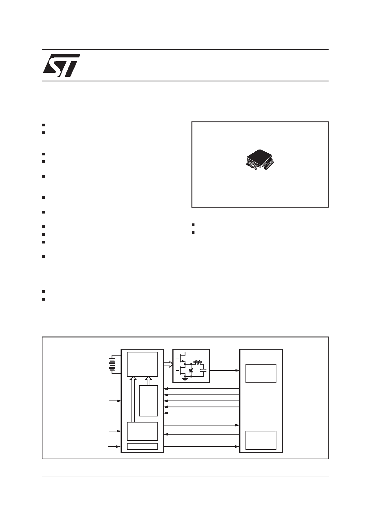
L5996
PRELIMINARY DATA
TQFP32
(7mm x 7mm)
Application
ADVANCEDMICROPROCESSORSUPPLIES
POWERSUPPLYFOR PENTIUM
BILE
DESCRIPTION
The L5996is a powersupply controller that offers
a complete power management for notebook
CPUs of the nextgenerationespecially for mobile
Pentium III. A high precise 5 bit digital to analog
converter (DAC) allows to adjust the output voltage from 0.925V to 2.0V. Dynamic DAC code
changes are detected on chip in order to switch
the output voltage between 1.3V and 1.45V in
less tahn 100µs.The high precision internal refer-
III INTEL MO-
TYPICALAPPLICATIONCIRCUIT
L5996
4.75V
FREQ
25V
SETTING
SYNC
NOSKIP
3.3V
to
PWM SECTIONS
DAC
POWER
MANAGEMENT
&
SYSTEM
SUPERVISOR
2.5V LIN. REG.
July 1999
This is preliminary information on a new product now in development or undergoing evaluation. Details are subject to change without notice.
POWER
SECTION
D0
D1
D2
D3
D4
POWER GOOD
ENABLE
2.5V
D98IN997A
V
O
0.925V to 2.0V
CPU CORE
PentiumIII
Mobile
CPU CLK
1/9
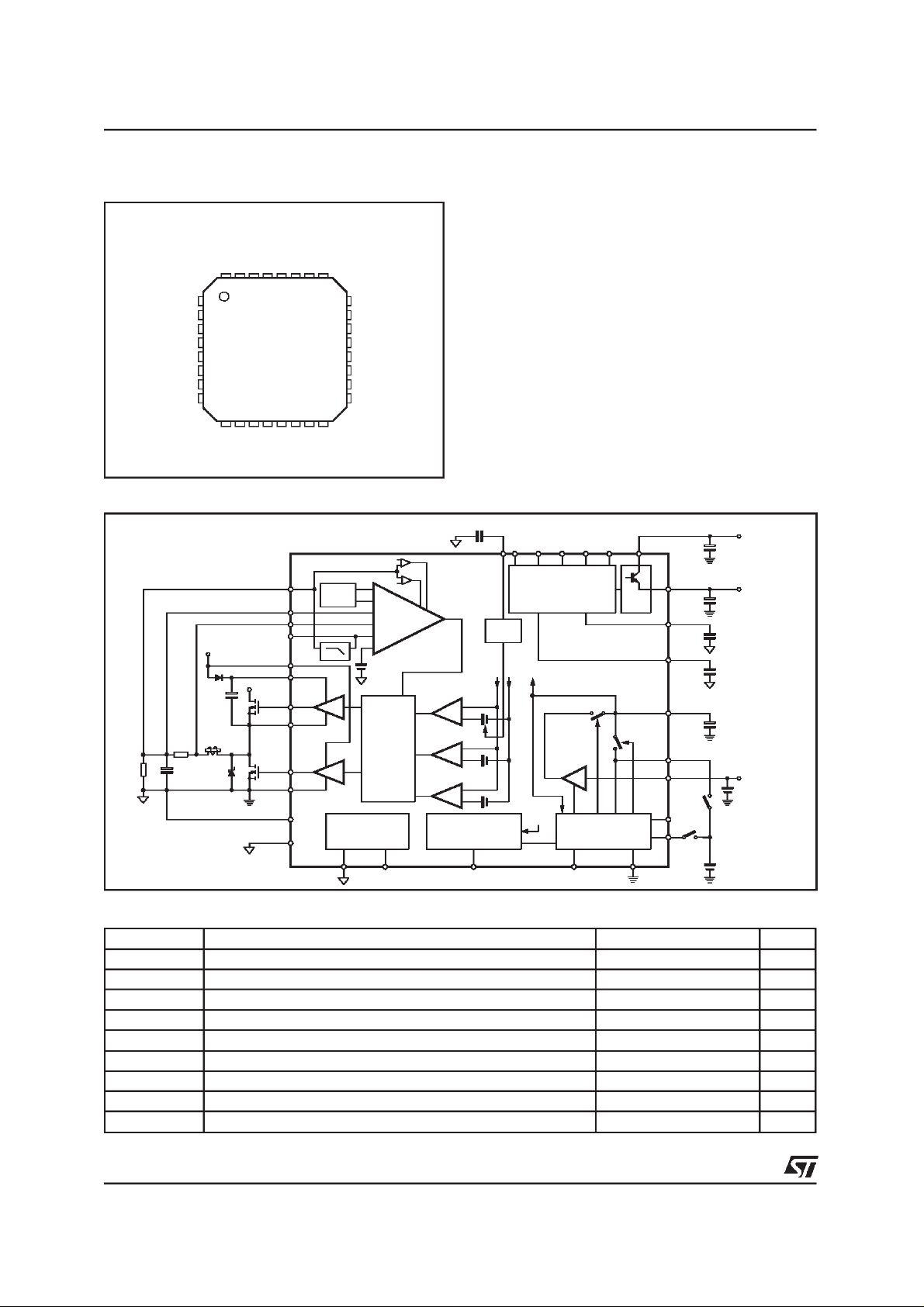
L5996
PIN CONNECTION
32 3031 29 28 27 26 25
1
ENABLE
2
VIN
3
REG5
4
V5SW
SSTART
HRSNS
LRSNS
5
6
7
8
910
DISPROT
BLOCK DIAGRAM
REG5
Cboot
Rsense
L
C
Load
POWERGOOD
RGATE
PWRGND
RSTRAP
11 12 13 14 15 16
VFB
COMP
VPROG
SNSGND
LRSNS
HRSNS
COMP
RSTRAP
HSTRAP
VIN
HGATE
HSRC
PWRGND
SNSGND
VFB
VSS
HSTRAP
HGATE
O2.5
IN2.5
V
V
9
8
7
10
29
28
27
26
30RGATE
31
12
16
HSRC
VBG
NOSKIP
24
23
22
21
20
19
18
17
VSS
SLOPE
Hside
Lside
OSC
VID4
VID3
VID2
VID1
VID0
ICURLIM
OSC
FREQ
D98IN998
OSCILLATOR
and
SYNC
18 17
+
-
-
ERROR
SUMMING
+
+
-
VPROG
CONTROL
LOGIC
FREQ
WINDOW
COMP
OVER CURRENT
COMPARATOR
+
-
ZERO
CROSSING
COMPARATOR
+
-
SKIPPING
PULSE
COMPARATOR
+
-
OVER/UNDER
COMPARATOR
19
ICURLIM
DESCRIPTION
(Continued)
ence, digitallytrimmed, assuresthe selected output voltage to within +/-1%over temperature and
battery voltage variations.
Thanks to the remote sensing inputs and to the
window comparator system,embedded in the error summing structure, the device provides excellent load transient performance. The high peak
current gate drive affords to have fast switching
to the externalpower mos, performing an high efficiency. A complete power management include
on board a programmable power-up sequencing,
power good signal, skip mode operation and undervoltege detection. The L5996 assures a fast
protection against load overvoltage and load
overcurrent. Linear regulator on-board is available with an output voltage of 2.5V (+/-2%) and a
current capability of 150mA, useful for CPU
CLOCK BUS.
CSOFT
SSTART
6
SOFT
START
HRSNS LRSNS
VOLTAGE
D98IN999
VID0 VID1 VID2 VID3
20 21 22 23
PROGRAMMABLE
BANDGAP
&
REFERENCE
INTERNAL SUPPLY
LINEAR
REGULATOR
VPROG
MANAGEMENT
25
NOSKIP
VID4
POWER
DISPROT
V
IN2.5
24
13
V
14
LIN.
11
32
3
4
2
1
O2.5
VBG15
VPROG
REG5
C5
V5SW
VIN
PWGOOD
ENABLE
2.5V
REG.
5
Vdc
5.5V to 25V
5V
V
IN3.3V
VCPUCLK
ABSOLUTE MAXIMUM RATINGS
Symbol Parameter Value Unit
VIN to PWRGND -0.5 to 27 V
PWRGND to VSS ±0.5 V
VREFS to PWRGND 5 V
HSTRAP, HGATE to PWRGND -0.5V to VIN+14V
RSTRAP, RGATE to PWRGND -0.5V to 14V
EABLE, FREQ, OSC, COMP, VFB, HRSNS, LRSNS 5 V
VID0-3, NOSKIP 7 V
Junction Temperature Range -40 to 150 °C
Storage Temperature Range -55 to 150 °C
2/9
T
j
T
stg
THERMAL DATA
Symbol Parameter Value Unit
R
Th j-amb
Thermal Resistance Junction to Ambient 60 °C/W
L5996
ELECTRICALCHARACTERISTICS
•
= specifications referred to TJfrom0 to 70°C.
= 12V; Ti=25°C,OSC = GND,unless otherwise specified)
(V
IN
Symbol Parameter Test Conditions Min. Typ. Max. Unit
DC CHARACTERISTICS
V
Input Supply Voltage • 4.75 25 V
IN
Operating Quiescent Current RGATE = HGATE =OPEN
I
OP
•
0.9 1.1 mA
ENABLE = REG5
I
Stand-By Current ENABLE = GND
SB
VIN = 12V
V
= 25V
IN
•
80
100
150
180
INTERNAL REGULATOR (VREG5)
V
I
REG5
Output Voltage VIN= 7.5V to25V
REG5
Total Current Capability CREG5 = 4.7µF
I
LOAD
C
REG5
V
IN
V
IN
=0 to 5mA,
= 4.7µF
= 5.5V
≥ 6V
4.9 5.0 5.1 V
25
60
Switch-Over Threshold Voltage 4.3 4.5 4.7 V
Current Capability
(internal switch on)
V
V
5SW
REG5
= 4.5 to5.5V
≥ 4.4V
25 mA
2.5V REFERENCE VOLTAGE
V
O 2.5
I
VO 2.5 MAX
Regulated Voltage V
Regulation over Lineand Load 6V < V
Current Limit V
= 3.3V
IN 2.5
C
=47µF
VO 2.5
I
= 10mA
O2.5
< 25V
IN
V
= 3.3V
IN 2.5
I
= 0-150mA
O2.5
= 3.3V 500 mA
IN 2.5
• 2.45 2.5 2.55 V
• 2.425 2.5 2.575 V
PROGRAMMABLE REFERENCE VOLTAGE AND VBG
V
PROG
Accuracy V
ID0,VID1,VID2,VID3,VID4
•
-0.5% V
PROG
+0.5% V
see Table 1.
V
V
Ouput Voltage Accuracy Line andLoad Regulation
FB
included, V
V
, see Table 1.
ID4
Band Gap reference C
BG
VBG
= 220nF
ID0,VID1,VID2,VID3
• -1% V
,
•
1.240 1.246 1.252 V
PROG
+1% V
POWER MANAGEMENT
Enable Voltage HIGH LEVEL 2.4 V
Disable Voltage LOW LEVEL 0.8 V
Power Good Saturation
= 400µA 0.4 V
I
sink
Voltage
NOSKIP Mode (Active high) High Level
0.8 V
Low Level 2.4
Output UVLO Threshold OVP = GND 60 70 80 %
Output UVLO Lockout Time Depending on C
value 775 ms/µF
SS
µ
µA
mA
mA
V
A
3/9

L5996
ELECTRICALCHARACTERISTICS
(continued)
Symbol Parameter Test Conditions Min. Typ. Max. Unit
PROTECTION FUNCTIONS
V
Over-Current Threshold
8-V7
V
SSTART
= 3.1V • 48 60 72 mV
Voltage
Pulse Skipping Mode
NOSKIP = HIGH 7 11 15 mV
Threshold Voltage
Zero Crossing Threshold -4 +4 mV
Under-Voltage Threshold Vprog
-13%
Upper Over-Voltage Threshold Vprog
+7%
Vprog
-10%
Vprog
+10%
Vprog
-7%
Vprog
+13%
Lower Over-Voltage Threshold Vprog
-4.5%
Over-Voltage Propagation
1.5 µs
Time
Under-Voltage Propagation
1.5 µs
Time
SOFT START
Soft start source current 3.2 4 4.8
Soft start clamp voltage 3.1 V
OSCILLATOR ANDSYNC
f
f
SINK MIN
Fixed frequency OSC =0V;FREQ = REG5 • 225 250 275 KHz
osc
• 180 200 220 KHz
Minimum Synchronizzable
external frequency
OSC = REG5 FREQ = REG5
FREQ = REG5
OSC = EXTERNAL SIGNAL
120 KHz
Sync pulse width Rising edge mode 200 ns
Sync pulse amplitude 3 5.5 V
fosc Operating switching frequency Rext connected between
•
FREQ and GND, OSC
connect to REG5 or GND
Rext = 680kΩ
Rext = 40kΩ
100
1
HIGH AND LOW SIDE GATE DRIVERS
I
Output high source peak
OH5
HSTRAP = RSTRAP =REG5 550 mA
current
R
Output high sink impedance I
H5
= 100mA,
test
3.5 Ω
HSTRAP = RSTRAP =REG5
I
OH12
Output high source peak
HSTRAP = RSTRAP =12V 2 A
current
R
Output high sink impedance I
H12
= 100mA,
test
2
HSTRAP - RSTRAP = 12V
I
R
Output low peakcurrent HSTRAP = RSTRAP =5V 500 mA
OL5
Output low impedance Itest = 100mA,
L5
3 Ω
HSTRAP = RSTRAP =5V
I
OL12
R
Output low peakcurrent HSTRAP = RSTRAP =12V 2 A
Output low Impedance I
L12
= 100mA,
test
2 Ω
HSTRAP = RSTRAP =12V
T
Dead Time GATE low to high 60 ns
CC
V
V
V
A
µ
kHz
MHz
Ω
4/9

L5996
FUNCTIONAL PIN DESCRIPTION
ENABLE(pin1): Enable input. A high level
(>2.4V) enables the device, a low level (<0.8V)
shuts it down. As ENABLE drops below 0.8V, the
drivers are turned off andall internalfunctionsare
disabled except REG5. In this condition the stand
by current is lessthan 80µA at VIN = 12V.
VIN(pin2):
Device supply voltage. Input voltage
range at this pin is 4.75V to 25V and the operating current requirementat 12V is 650µA.
REG5(pin3): 5V Regulator supply. Used also to
supply the bootstrap capacitor. A minimum 2.2µF
ceramic capacitor connected to PWRGND is required.
V5SW(pin4): 5V supply line. Connecting to 5V
bus(4.75V to 5.5V) the device is no longer powered by VIN but by this pin and the internal linear
regulator is disconnected increasing the efficiency.
DISPROT (pin5) Disable Protection Functions. A
high level (3.3V CMOS LOGIC) on this pin disables the undervoltage and the overvoltage pro-
SS
tection. Tie thispin to V
for normaloperation.
VPROG(pin11): Reference voltage test pin. This
pin provides the DAC output and should be decoupled to ground using a 0.22µF ceramic ca-
pacitor. No load hasto be connected.
SNSGND(pin12):
Remote ground sense. This
pin is internally connected to the low power circuitry and for a precise output voltage regulation
can be connected to the output capacitor negative terminal.
(pin13): 2.5V linear supplyvoltage. Is avail-
V
IN2.5
able on-chip a linear regulator useful for the 2.5V
bus. A max input voltage of 3.3V is recommended at Iomax(150mA).
(pin14):
V
O2.5
2.5V linear regulator output. The
linear regulator is realised with an internal NPN
transistor with +/-2% output accuracy. A minimum of 47µF capacitor connected versus
PWRGND is required.
VBG(pin15):
Band-gap reference voltage. A min
220nF ceramic capacitor is requiredto assure the
band gap stabilityand noise immunity.
VSS(pin16):
Signal ground. This pin could be
connectedto the PWRGND pin.
SSTART(pin6): Soft Start. The soft-start time is
programmed by an external capacitor connected
between this pin and SGND. The internal current
generatorforces 4µA throughthe capacitor implementing the soft startfunction.
HRSNS(pin7): Error summing current sense non
inverting input.
LRSNS(pin8):
Error summing current sense in-
verting input.
VFB(pin9): Regulator voltage feedback input.
Connect close to the CPU input supply pin realise
an accurate voltage regulation. VFB internally is
connected to the window comparatorthat is used
to increasethe performanceduring the load transient.
COMP(pin10):
Regulator stability compensation
pin. The compensation is realised internally and
normally it is not necessaryto connect any external components to this pin.
FREQ(pin17): Connecting an external resistor
versus ground is possible to select the switching
frequency between 100kHz and 1MHz. Using an
Rext=680k the fsw is 100kHz, using an Rext =
40k the fsw is 1MHz. In this condition is recommended to connect the OSC pin to REG5 or to
VSS.
OSC(pin18):
Connecting to REG5 is able to set
the switching frequencyat 200kHz, connecting to
VSS is able to set the switching frequency at
250kHz. An external pulsed signal, withan amplitude higher than 2.4V, could synchronise the device. In all these conditions pin FREQ has to be
connectedto REG5.
OVP/CURLIM(pin19): Over voltage protection
and reduced current limit window. If the output
voltage reaches the 10% above the programmed
voltage (VPROG) this pin is driven low the high
side driver is turned off and the low, sidedriver is
turned on. All the internal blocks are active. The
device uses OVP function to dischargethe output
during HIGH_TO_LOW core voltage transition.
The pin is drivenlow alsoduring LOW_TO_HIGH
core voltage transition. The pin will stay low as
5/9

L5996
long as the current limit value is reduced with respect to the normal operating value. This is done
to limit voltage overshoots during core voltage
changes. Making this signal externally available
simplifiessystem debugging.
VID0-4(pin20-24):
Voltage Identification code input. These open collector compatible inputs are
used to program the output voltage as specified
in Table 1. Every pin has an internal pull up. If all
four pins are high or floating, the output voltage
and the 2.5V regulator are suspended and the
POWERGOODis low.
NOSKIP(pin25):
Pulse skipping mode control. A
high level (>2.4V) disables pulse skipping in low
load condition,a lowlevel (>0.8V)enables it.
HSRC(pin26):
High side N-Channel switch
source connection. This pin provides the return
path forthe high side driver.
HGATE(pin27): Gate driver output, high side NChannel switch. The driver internal impedance is
about 4Ωat VIN=12V.
HSTRAP(pin28):
Bootstrapcapacitor pin. This pin
provide to supply the high side driver sinking the
current by the bootstrapcapacitor.
RSTRAP(pin29):
Synchronous rectifier gate
driver supply voltage. This pin could be connected to REG5 to reduce the switching losses
due to the external Mosfets gate capacitance.
This is useful to maintain an high efficiency at
light load.
RGATE(pin30): Gate driver output, low side NChannel switch. The driver internal impedance is
about 3Ω at VIN=12V.
PWRGND(pin31):
Power ground. This pin has to
be connected closely to the low side mosfet
source in order to reduce the noise injected into
the IC.
POWER GOOD(pin32):
Open drain power good
output. This pin is pulled low if the output voltage
is not within ±10% and the 2.5V output is lower
than 2.175V (-13%). The pin is pulled low also if
REG5, VPROG and VBG have not reached the
expected values. This test could be useful in an
assemblingfault condition.
Table 1. VID [4:0] AND corresponding+VCC_CPU_CORE ranges
VID[4:0] +VCC_CPU_CORE VID[4:0] +VCC_CPU_CORE
00000 2.00V 10000 1.275V
00001 1.95V 10001 1.250V
00010 1.90V 10010 1.225V
00011 1.85V 10011 1.200V
00100 1.80V 10100 1.175V
00101 1.75V 10101 1.150V
00110 1.70V 10110 1.125V
00111 1.65V 10111 1.100V
01000 1.60V 11000 1.075V
01001 1.55V 11001 1.050V
01010 1.50V 11010 1.025V
01011 1.45V 11011 1.000V
01100 1.40V 11100 0.975V
01101 1.35V 11101 0.950V
01110 1.30V 11110 0.925V
01111 No CPU 11111 No CPU
6/9

Figure 1. ApplicationCircuit
Vin
4.5V to 25V
REG5 VIN RSTRAP
SSTART
3229
6
VBG
15
L5996
HSTRAP
28
HGATE
27
5V BUS
NOSKIP
DISPROT
Vin2
3.3V
D98IN1000B
VSS
OSC
FREQ
VPROG
V5SW
25
16
18
17
5
11
4
ICURLIM
L5996
20÷24
1
3219
26
30
31
12
1413
7
8
9
HSRC
RGATE
PWRGND
HRSNS
LRSNS
SNSGND
VFB
Vo2.5
PWRGOOD
ENABLE
VID
Vo
0.925V to 2.0V
5
PentiumIII
Mobile
Vo2
2.5V/150mA
Figure 2. Output voltage transition between1.3V and 1,5V measuredat 200mAload current.
CH1: VID 2transition.
CH2: Output voltage transition between 1.3V and 1.5Vmeasuredat 200mAload current.
7/9

L5996
DIM.
MIN. TYP. MAX. MIN. TYP. MAX.
A 1.60 0.063
A1 0.05 0.15 0.002 0.006
A2 1.35 1.40 1.45 0.053 0.055 0.057
B 0.30 0.37 0.45 0.012 0.015 0.018
C 0.09 0.20 0.004 0.008
D 9.00 0.354
D1 7.00
D3 5.60 0.220
e 0.80 0.031
E 9.00 0.354
E1 7.00
E3 5.60 0.220
L 0.45 0.60 0.75 0.018 0.024 0.030
L1 1.00 0.039
K 0°(min.),7°(max.)
mm inch
0.276
0.276
OUTLINE AND
MECHANICAL DATA
TQFP32
D
D1
D3
1724
25
B
32
1
16
E3
9
8
E1
E
0.10mm
.004
Seating Plane
e
L1
L
A1
B
C
A
A2
K
TQFP32
8/9

L5996
Information furnished is believed to be accurate and reliable. However, STMicroelectronics assumes no responsibility for the consequences
of use of such information nor for any infringement of patentsor other rights of third parties which may result from its use. No license is
granted by implication or otherwise under any patentor patent rights of STMicroelectronics. Specification mentioned in this publication are
subject to change without notice. This publication supersedes and replaces all information previously supplied. STMicroelectronics products
are not authorized for use as critical components in life support devices or systems without express written approval of STMicroelectronics.
The ST logo is a registeredtrademark of STMicroelectronics
1999 STMicroelectronics – Printedin Italy – All Rights Reserved
STMicroelectronics GROUP OF COMPANIES
Australia - Brazil - China- Finland- France - Germany - Hong Kong - India - Italy - Japan - Malaysia - Malta - Morocco -
Singapore - Spain - Sweden - Switzerland- UnitedKingdom - U.S.A.
http://www.st.com
9/9
 Loading...