

DUAL PWM BUCK CONTROLLERS
ADJUSTABLE
1.9V to 5V(Section 1)
1.66V to 3.5V (Section 2)
12V/120mALINEAR REGULATOR
DUALSYNCH RECTIFIERSDRIVERS
96%EFFICIENCYACHIEVABLE
50µA (@ 12V) STAND BY CONSUMPTION
5.0V TO 25V SUPPLY VOLTAGE
EXCELLENTLOAD TRANSIENTRESPONSE
DISABLEPULSE SKIPPINGFUNCTION
OUTPUTUNDERVOLTAGESHUTDOWN
POWERMANAGEMENT:
- UNDERAND OVERVOLTAGEOUTPUT
DETECTION
- POWER GOOD SIGNAL
- SEPARATEDDISABLE
THERMALSHUTDOWN
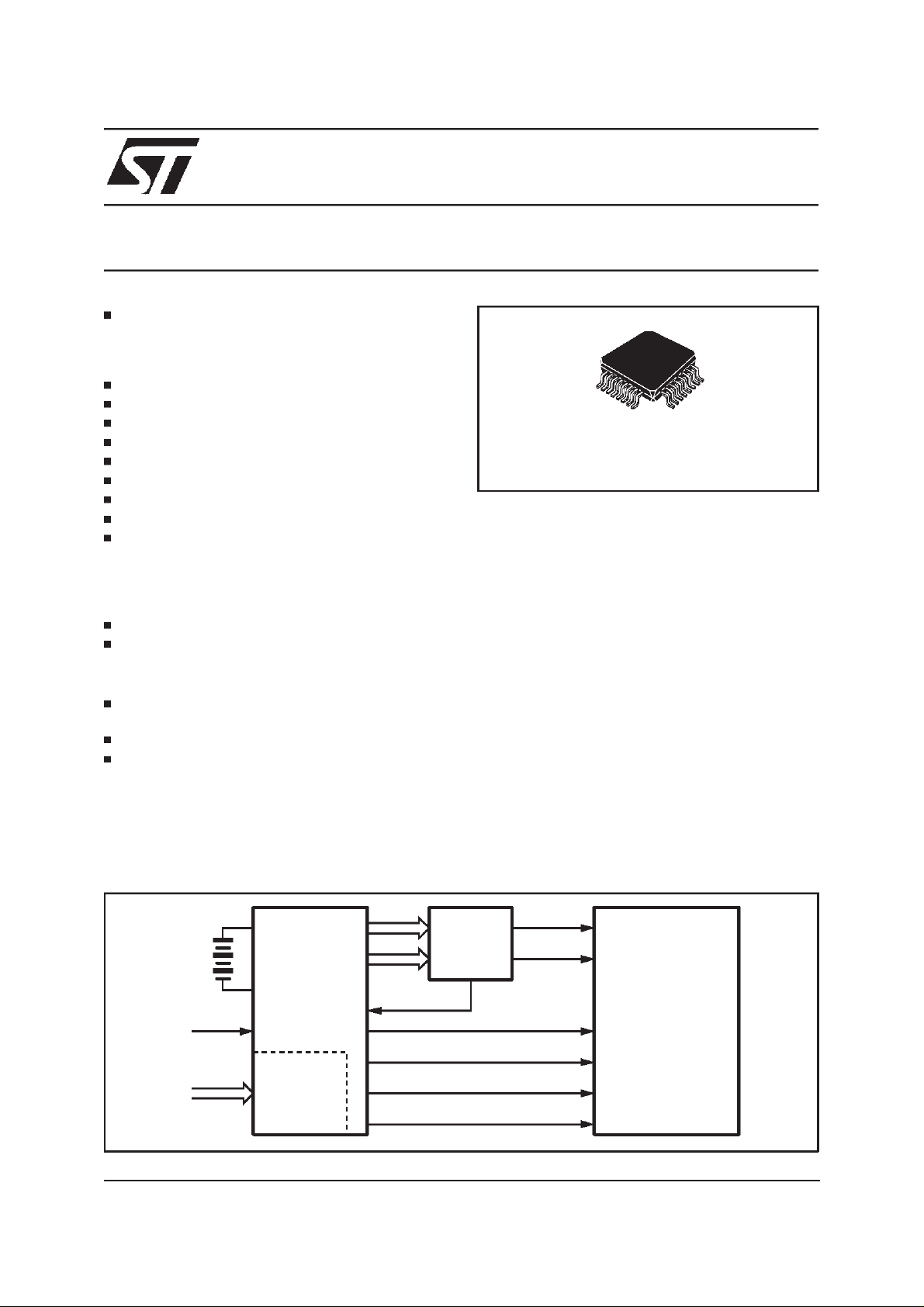
PACKAGE:TQFP32
APPLICATION
NOTEBOOK AND SUBNOTEBOOK COMPUTERS
PENTOP AND PORTABLE EQUIPMENT
COMMUNICATINGCOMPUTERS
DESCRIPTION
The L5994 is a sophisticated dual PWM stepdown controller and power monitor intended for
SYSTEM BLOCK DIAGRAM
L5994
ADJUSTABLETRIPLE OUTPUT
POWER SUPPLY CONTROLLER
PRODUCT PREVIEW
TQFP32
ORDERING NUMBER: L5994
Notebook computer and/or battery powered
equipment. The device produces regulated 1.8V,
2.5V (both adjustable)and 12V supplies for use in
portableand PCMCIA applications.
The internal architecture allows to operate with
minimum external componentscount. A very high
switching frequency (200/300 KHz or externally
synchronizable) optimizes their physical dimensions.
Synchronous rectification and pulse skipping
mode for the buck sections optimise the overall
efficiencyover a wide load current range.
The two high performance PWM controllers for
1.8V and 2.5V lines are monitored for overvoltage, undervoltage and overcurrent conditions.
On detection of a fault, a POWER GOOD signal
is generated and a specific shutdown procedure
takes place to preventphysical damage and data
corruption.
A disable function allows to manage the output
power sections separately, optimising the quiescent consumptionof theIC in stand-byconditions.
2.5V
5V
to
25V
L5994
POWER
SECTION
1.8V
µP
SYNC
POWER
MANAGEMENT
& SYSTEM
SUPERVISOR
D98IN862
September 1999
This is preliminary information on a new product now in development. Details are subject to change withoutnotice.
12V LDO
5.1V LDO
3.39V REF
POWER GOOD
MEMORY
PERIPHERALS
1/8
L5994
ABSOLUTE MAXIMUM RATINGS
Symbol Parameter Value Unit
V
I
OUT
IN
V
I
I
IN
T
J
Power Supply Voltage on V
IN
Maximum Pin Voltage to Pins 1, 24, 25, 32 -0.5 to (VIN+5) V
Input Current Except V13IN and V
IN
Output Current Digital Output -15 to +15 mA
Junction Temperature -55 to 150 °C
THERMAL DATA
Symbol Parameter Value Unit
R
TH J-amb
Thermal Resistance Junction -Ambient 60 °C/W
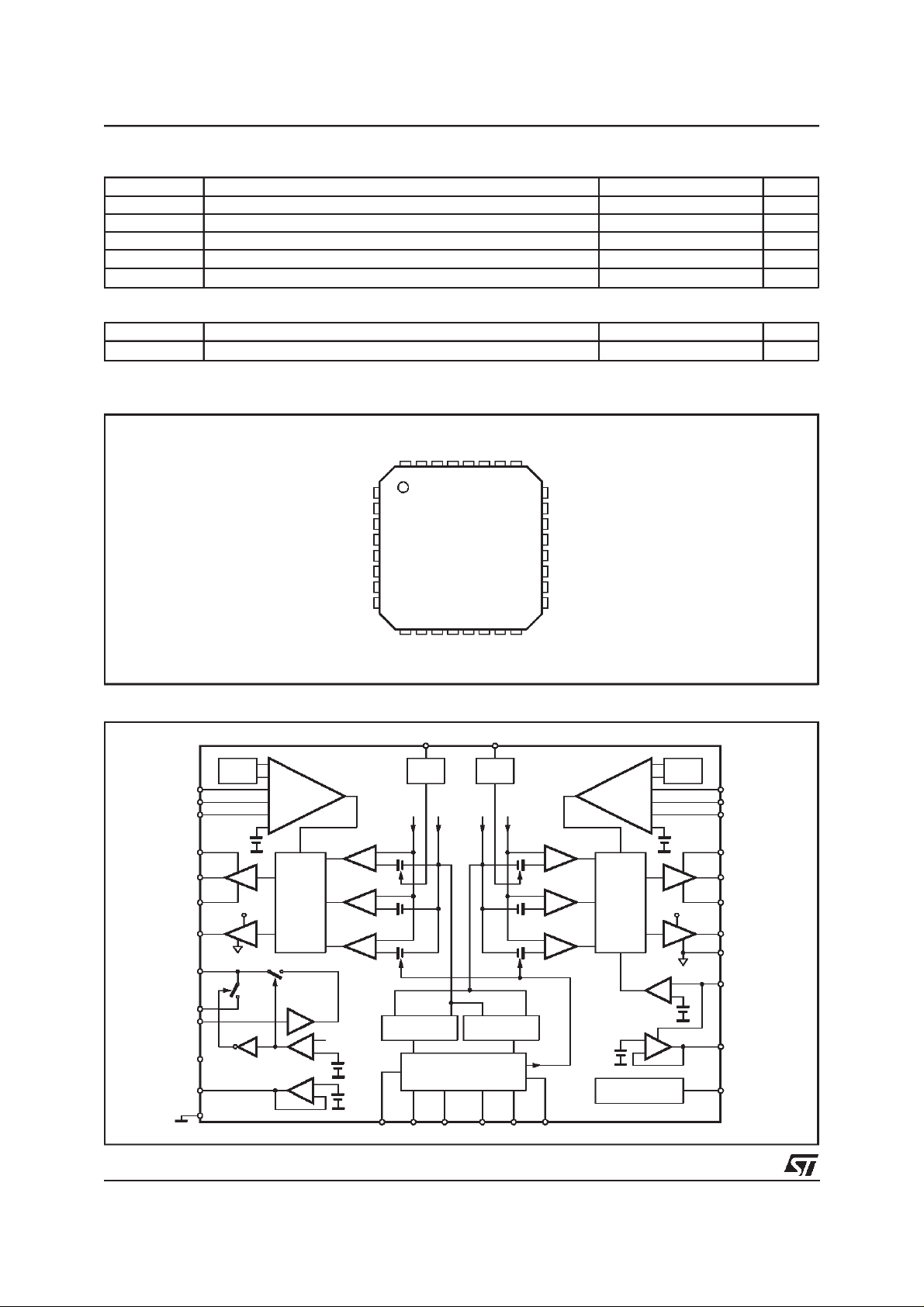
PIN CONNECTION(Topview)
H1GATE
R1GATE
H1SRC
PREG5
PGND
R2GATE
H2SRC
H2GATE
32 3031 29 28 27 26 25
H1STRAP
VIN
SREG5
V5SW
V1SNS
I1SNS
COMP1
SOFT1
1
2
3
4
5
6
7
8
11 12 13 14 15 16
910
24
23
22
21
20
19
18
17
H2STRAP
PWROK2
REG12
V13IN
V2SNS
I2SNS
COMP2
SOFT2
0to25 V
-1 to +1 mA
BLOCK DIAGRAM
6
I1SNS
5
V1SNS
7
COMP1
1
H1STRAP
32
H1GATE
31
H1SRC
30
R1GATE
PREG5
29
4
W5SW
2
VIN
SREG5 3
12VREF
SGND
13
SGND
SOFT2
SOFT
UNDERVOLT
COMPARATOR
&
OSC
NOSKIP
17
I2SNSV2SNS
RUN2
OVER
COMPARATOR
ZERO
COMPARATOR
PULSE
COMPARATOR
PWROK2
ERROR SUMMING
CURRENT
+
CROSSING
+
-
SKIPPING
+
-
VREF
23
+
-
+
∑
-
+
-
VREF
CONTROL
LOGIC
13V UVComp
13V
+
-
OSCILLATOR
SYNCHRONIZATION
RUN1
VREF
CRST
PWROK1
SOFT1
+
SLOPE
VREF
Hside
REG5 PREG5
Lside
COMPARATOR
VREF BUFFER
-
+
-
+
-
CONTROL
SWITCH
ERROR SUMMING
∑
LOGIC
LINEAR
REGULATOR
-
+
+
-
CURRENT
OVER
COMPARATOR
ZERO
CROSSING
COMPARATOR
PULSE
SKIPPING
COMPARATOR
V5SW
4.7V
VREF
+
+
+
8
SOFT
I1SNS V1SNS
-
-
-
OVERVOLT
COMPARATOR
MANAGEMENT
POWER
SYSTEMSUPERVISOR
16 11 10 14 9
RUN2 RUN1 PWROK1 NOSKIP CRST
D98IN863A
&
Hside
Lside
+
-
SLOPE
D98IN864
REG12
LDO
19
20
18
24
25
26
27
28
21
22
15
I2SNS
V2SNS
COMP2
H2STRAP
H2GATE
H2SRC
R2GATE
PGND
V13IN
REG12
OSC
2/8
PIN FUNCTIONS
N. Name Description
1 H1STRAP Section 1 section bootstrap capacitor connection
2V
3 SREG5 Signal 5V. It should be connected to PREG5 pin.
4 V1SW Alternative device supply voltage.
5 V1SNS Thispin connects to the (-) input of the section 1 internal current sense comparator
6 I1SNS This pin connects to the (+) input of the section 1 internal current sense comparator
7 COMP1 Feedback input for the section 1.
8 SOFT1 Soft-start input of the section 1. The soft-start time is programmed by an external capacitor
9 CRST Input used for start-up and shut-down timing. A capacitor defines a time of 2ms/nF.
10 PWROK1 Power-good diagnostic signal. This output is driven high when section 1 is enabled and
11 RUN1 Control input to enable/disable the section 1. A high level (>2.4V) enables this section, a low
12 VREF Internal +2.5V high accuracy voltagegenerator. It can source 5mA to external load. Bypass to
13 SGND Signal ground. Reference for internal logic circuitry. It must be routed separately from high
14 NOSKIP Pulse skipping mode control. A high level (>2.4V) disables pulse skipping at low load current,
15 OSC Oscillator frequency control: connect to 2.5V to select 300KHz operation, to ground or to 5V
16 RUN2 Control input to enable/disable the section 2. A high level (>2.4V) enables this section, a low
17 SOFT2 Soft-start input for thesection 2. The soft-start time is programmed by an external capacitor
18 COMP2 Feedback input for the section 2.
19 I2SNS This pin connects to the (+) input of the section 2 internal current sense comparator
20 V2SNS This pin connects to the (-) input of the section 2 internalcurrent sense comparator
21 V13IN 12V regulator input supply voltage, included between 13 and 20V. This voltage can be
22 REG12 12V regulatoroutput voltage. It can source up to 150mA toan external load
23 PWROK2 Power good diagnostic signal. This output is driven high when section 2 is enabledand
24 H2STRAP Section 2 bootstrap capacitor connection
25 H2GATE Gate- driver output for the section 2high-side N-MOS
26 H2SRC Section 2 high-side N-MOS source connection
27 R2GATE Gate- driver output for the section 2low- side N-MOS (synchronous rectifier).
28 PGND Current return for drivers
29 PREG5 +5V regulator supply. Used mainly for bootstrap capacitors. It should bebypassed to ground.
30 R1GATE Gate-driver output for the section 1 low-side N-MOS (synchronous rectifier).
31 H1SRC Section 1 high-side N-MOS source connection
32 H1GATE Gate-driver output for the section 1 high-side N-MOS
IN
Device supply voltage. From 5.0 to 25V
connected between this pin and SGND. Approximately, 1ms/nF @ full load.
running properly, after a delay defined by the CRST capacitor.
level (<0.8V) shuts it down
ground with a 4.7µF capacitor to reduce noise.
current returns.
a low level (<0.8V) enables it.
for 200KHz operation. A proper external signal can synchronize the oscillator
level (>0.8V) shuts it down.
connected between this pin and GND. Approximately, 1ms/nF @full load.
supplied by a flyback winding.
running properly, after a delay defined by CRST capacitor
L5994
3/8

L5994
ELECTRICALCHARACTERISTICS
IN
= 12V; TJ=25°C;V
(V
OSC
= GND; unless otherwise specified.)
Symbol Parameter Test Condition Min. Typ. Max. Unit
DC CHARACTERISTICS
V
IN
I
2
I
2
Input Supply Voltage 5.0 25 V
Operating Quiescent Current R1GATE= R2GATE = OPEN
1.35 mA
H1GATE = H2GATE = OPEN
RUN2 = RUN1 = SREG5
(DRIVERS OFF)
Stand-By Current RUN2= RUN1 = GND
V
= 12V
IN
V
IN = 20V
50
60
100
120
SECTION1 PWM CONTROLLER
V
(*) V1SNS Feedback Voltage VIN= 5.0 to 20V;
1OUT
V
6-V5
V
6-V5
Over-Current Threshold Voltage VSOFT1 = 4V 50 mV
Pulse Skipping Mode
Thereshold Voltage
V
5
Over VoltageThreshold ON
V
I1SNS-VV1SNS
VIN> 6.8V 13 mV
< 5.8V 6.5 mV
V
IN
= 0 to 40mV
1.843 1.9 1.957 V
1.99 2.052 2.11 V
V1SNS
Under Voltage Threshold ON
1.695 1.748 1.80 V
V1SNS
SECTION2 PWM CONTROLLER
V
(*) V2SNS Feedback Voltage VIN= 5.0 to 20V;
2OUT
V
19-V20
V
19-V20
Over Current Threshold Voltage VSOFT2 = 4V 50 mV
Pulse Skipping Mode Threshold
V
I2SNS-VV2SNS
VIN= 5.0 to 20V; 13 mV
Voltage
V
20
Over VoltageThreshold ON
V2SNS
Under Voltage Threshold ON
V2SNS
= 0 to 40mV
1.610 1.66 1.709 V
1.738 1.792 1.845 V
1.48 1.527 1.572 V
µA
PWMCONTROLLERS CHARACTERISTICS (BOTH SECTIONS)
F
OSC
V
15
T
OFF
T
OV
T
UV
V
5,V20
I
8,I17
V
8,V17
(*) Guaranteed by design,not tested in production
4/8
Switching Frequency Accuracy OSC = SREG5/2 255 300 345 kHz
OSC = 0 or SREG5 170 200 230 kHz
Voltage Range for 300kHz
Operation
Dead Time 300 375 450 ns
Overvoltage Propagation Time V1SNS to PWROK or
V2SNS to PWROK
Undervoltage Propagation Time V1SNS to PWROK or
V2SNS to PWROK
Output UVLO Threshold Respect output voltage 70 %
Soft Start Charge Current 3.2 4 4.8
Soft Start Clamp Voltage 4 V
2.4 2.6 V
1.25 µs
1.5
µ
s
µ
A

L5994
ELECTRICALCHARACTERISTICS
(Continued)
Symbol Parameter Test Condition Min. Typ. Max. Unit
HIGH AND LOW SIDE GATE DRIVER (BOTH SECTIONS)
I25,I
I32,I
R
R
V
V
T
H
L
OH
OL
CC
Source Output Peak Current C
27,
30
Sink Output Peak Current C
R
Resistance(orImpedance) DriverOUT HIGH 7
DSON
R
resistance(or Impedance) Driver OUT LOW 5 Ω
DSON
Output High Voltage HSTRAP = PREG5
= 1nF 0.2 0.5 A
LOAD
= 1nF 0.2 0.5 A
LOAD
4.40 5.3 5.61 V
I
= 10mA; HSRC = GND
SOURCE
Output Low Voltage HSTRAP = PREG5
I
= 10mA HSRC = GND
SINK
Cross-Conduction Delay 30 75 130 ns
0.5 V
12V LINEARREGULATOR SECTION
V
21
V
22
I
22
V
CP
Input Voltage Range 13 20 V
Output Voltage I22= 0 to 120mA 11.54 12.0 12.48 V
Current Limiting V
Short Circuit Current V
Input Voltage Clamp I
”One Shot” Activation Threshold V
= 12V 120 mA
REG12
= 0V 150 mA
REG12
= 100µA16 V
CLAMP
Falling 12.88 13.7 14.52 V
13IN
”One Shot” Pulse 1.5 µs
INTERNALREGULATOR (VPREG5) AND REFERENCE VOLTAGE
V
29
I
29
V
12
I
12
VREG5 Output Voltage VIN= 5.0 to 20V
I
= 0 to 5mA
LOAD
Total Current Capability VPREG5 = 5.3V
V
=6V
REG5
5.0 5.3 5.61 V
25
70
Switch-Over Threshold Voltage 4.3 4.53 4.7 V
Reference Voltage 2.5 V
IN = 5.0 to 20V
Source Current at Reference
V
I
LOAD
= 1 to 5mA
5mA
2.5 V
Voltage
Ω
mA
POWER GOOD AND ENABLE FUNCTION
V16,V
V
16,V11
T
10
T
27,T30
SYNCHRONIZATION
RUN2, RUN1, Enable Voltage HIGH LEVEL 2.4 V
11
RUN2, RUN1, Disable Voltage LOW LEVEL 0.8 V
Power Good Delay CCRST = 100nF 160 200 240 ms
Shutdown Delay Time before
Low Side Activation
(Except Over-Voltage Fault)
CRST Timing Rate 2 ms/nF
Power Good High Level I
Power Good LowLevel I
Synchronisation Pulse Width 400 ns
Synchronisation Input Voltage
(Falling Edge Transition)
C
= 100nF, 160 200 240 ms
CRST
=40µA 4.1 V
PWROK
= 320µA 0.4 V
PWROK
5V
5/8

L5994
APPLICATIONCIRCUIT
C25
C13
C14
R20
C15
GND
VOUT3 12V
PWROK2
GND
R7
R8
C27
D98IN866A
R16
C4C8
D4
SREG5
VIN
D3
R18 C29
H2STRAP
24
32
1
H1STRAP
Q3
H2GATE
25
32
H1GATE
Q1
C19
R3
R4
C17
H2SRC
26
L2/T2
Q4
R2GATE
27
D2
PIN29
R9
C21 C23 C24C22
PGND
I2SNS
V13IN
V2SNS
COMP2
20
19
28
PWROK2
REG12
SOFT1
SOFT2
CRST
VREF
8
18
23
9
17
12
SGND
D5
L5994
312130
H1SRC
C16
R1GATE
Q2
2965137224
PREG5
G1
I1SNS
G2
V5SW
V1SNS
COMP1
PIN29
10
PWROK1
OSC
15
RUN2
141116
RUN1
NOSKIP
6/8
VIN
R33
C2
C1 C7
C6 C3
GND
R17
C28
PIN21
D1
L1/T1
D6
R1
R2
C9
C10
C11
C26
R19
VOUT1 VOUT2
GND
R34
R5
+5VIN
R6
C18 C20
GND
R13 R12 R11 R10
R15
PWROK1
R14 S2 S1 S3 S4
NOSKIP

L5994
DIM.
MIN. TYP. MAX. MIN. TYP. MAX.
A 1.60 0.063
A1 0.05 0.15 0.002 0.006
A2 1.35 1.40 1.45 0.053 0.055 0.057
B 0.30 0.37 0.45 0.012 0.015 0.018
C 0.09 0.20 0.004 0.008
D 9.00 0.354
D1 7.00
D3 5.60 0.220
e 0.80 0.031
E 9.00 0.354
E1 7.00
E3 5.60 0.220
L 0.45 0.60 0.75 0.018 0.024 0.030
L1 1.00 0.039
K 0°(min.), 7°(max.)
mm inch
0.276
0.276
OUTLINE AND
MECHANICAL DATA
TQFP32
D
D1
D3
1724
25
B
32
1
16
E3
9
8
E1
E
0.10mm
.004
SeatingPlane
e
L1
L
A1
B
C
A
A2
K
TQFP32
7/8

L5994
Information furnished is believed to be accurate and reliable. However, STMicroelectronics assumesno responsibility for the consequences
of use of such information nor for any infringement of patents or other rights of third parties which may result from its use. No license is
granted by implication or otherwise under any patent or patent rights of STMicroelectronics. Specification mentioned in this publication are
subject to change without notice. This publication supersedes and replaces all information previously supplied. STMicroelectronics products
are not authorized for use as critical components in life support devices or systems without express written approval of STMicroelectronics.
The ST logo is a registered trademark of STMicroelectronics
1999 STMicroelectronics – Printed in Italy – AllRightsReserved
STMicroelectronics GROUP OF COMPANIES
Australia - Brazil - China- Finland - France - Germany - HongKong - India - Italy - Japan - Malaysia - Malta - Morocco -
Singapore - Spain - Sweden - Switzerland - United Kingdom - U.S.A.
http://www.st.com
8/8
 Loading...