

L5993
CONSTANT POWER CONTROLLER
CURRENT-MODECONTROLPWM
SWITCHINGFREQUENCYUP TO 1MHz
LOW START-UPCURRENT (< 120µA)
CONSTANT OUTPUT POWER VS. SWITCH-
ING FREQUENCY
HIGH-CURRENT OUTPUT DRIVE SUITABLE
FOR POWERMOSFET (1A)
FULLY LATCHED PWM LOGIC WITH DOU-
BLE PULSE SUPPRESSION
PROGRAMMABLEDUTYCYCLE
100%AND50%MAXIMUMDUTYCYCLELIMIT
PROGRAMMABLE SOFT START
PRIMARY OVERCURRENT FAULT DETEC-
TION WITH RE-START DELAY
PWMUVLOWITH HYSTERESIS
IN/OUTSYNCHRONIZATION
LATCHEDDISABLE
INTERNAL 100ns LEADING EDGE BLANK-
ING OF CURRENT SENSE
PACKAGE:DIP16 ANDSO16N
DESCRIPTION
This primary controllerI.C., developed in BCD60II
technology, has been designed to implement off
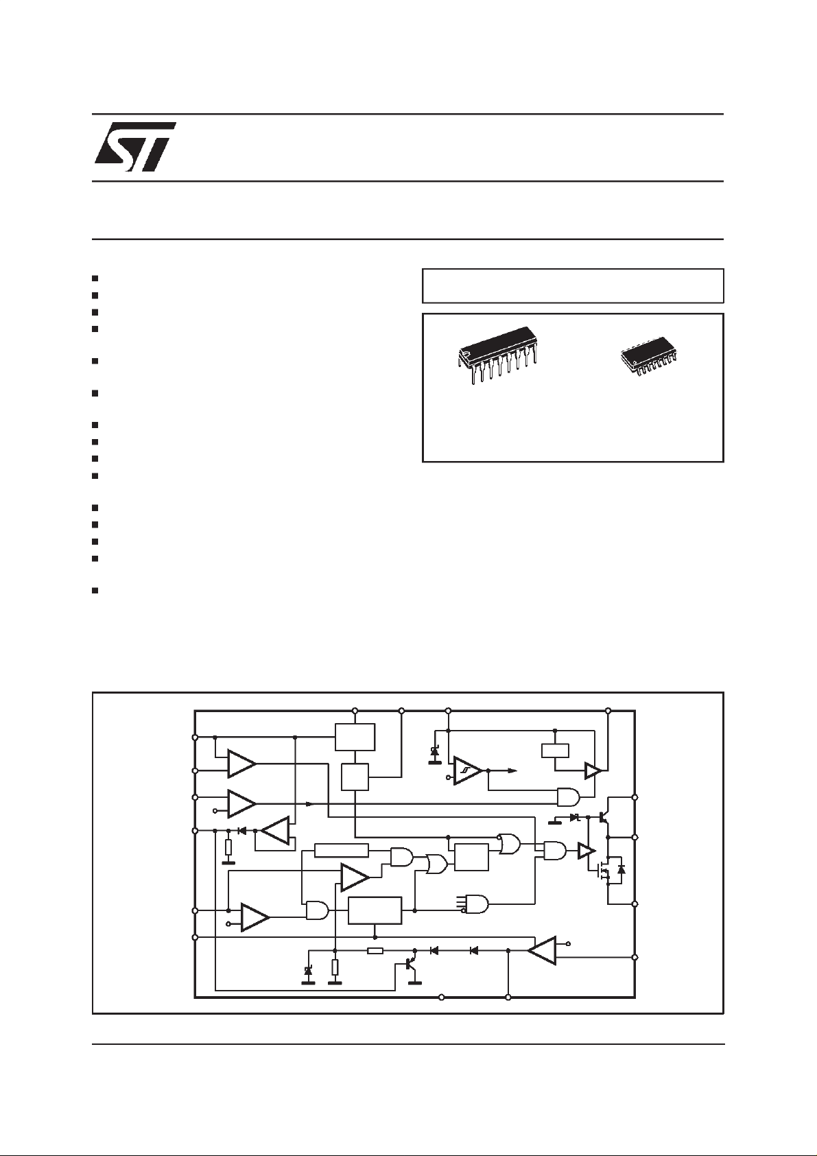
BLOCK DIAGRAM
MULTIPOWER BCD TECHNOLOGY
DIP16 SO16N
ORDERING NUMBERS: L5993 (DIP16)
L5993D (SO16)
line or DC-DC power supply applications using a
fixedfrequencycurrentmode control.
Based on a standard current mode PWM controller this device includes some features such as
programmablesoft start, IN/OUT synchronization,
disable (to be usedfor over voltage protection and
for power management), precise maximum Duty
Cycle Control, 100ns leading edge blanking on
current sense, pulse by pulse current limit, overcurrent protection with soft start intervention and
”constantpower” functionfor cotrolling throughput
powerin multisyncmonitorSMPS.
July 1999
RCT
DIS
C-POWER
ISEN
SYNC DC-LIM
2
+
3
14
2.5V
13
1.2V
-
-
+
+
-16
OVER CURRENT
+
-
1V R
DC
SS
DIS
TIMING
BLANKING
PWM
T
FAULT
SOFT-START
2R
V
CC
25V
15V/10V
+
-
SQ
R
VREF OK
CLK
DIS
12
SGND COMP
PWM UVLO
6
Vref
+
E/A
-
13V
2.5V7
D97IN765
VREF
48151
9
V
C
10
OUT
11
PGND
5
VFB
1/22
L5993
ABSOLUTEMAXIMUM RATINGS
Symbol Parameter Value Unit
V
CC Supply Voltage (I
I
OUT
Output Peak Pulse Current 1.5 A
Analog Inputs & Outputs (6,7) -0.3 to 8 V
Analog Inputs & Outputs (1,2,3,4,5,15,14,13, 16) -0.3 to 6 V
P
tot
T
j
T
stg
(*) maximum package power dissipation limits must be observed
Power Dissipation @ T
Junction Temperature, Operating Range -40 to 150 °C
Storage Temperature, Operating Range -55 to 150 °C
PIN CONNECTION
< 50mA) (*) selflimit V
CC
@T
=70°C (DIP16)
amb
=50°C (SO16)
amb
1
0.83
W
W
SYNC
RCT
DC
VREF
VFB
COMP
SS
V
CC
1
2
3
4
5
6
7 OUT
15
14
13
12
11
10
8V
D97IN783
C-POWER16
DC-LIM
DIS
ISEN
SGND
PGND
9
C
THERMAL DATA
Symbol Parameter Value Unit
R
th j-amb
Thermal Resistance Junction -Ambient(DIP16)
Thermal Resistance Junction -Ambient(SO16)
80
120
PIN FUNCTIONS
N. Name Function
1 SYNC Synchronization. A synchronization pulse terminates the PWM cycle and discharges Ct
2 RCT Oscillator pin for external C
3 DC Duty Cycle control
4 VREF 5.0V +/-1.5% reference voltage at 25°C
5 VFB Error Amplifier Inverting input
6 COMP Error Amplifier Output
7 SS Soft start pin for external capacitor Css
8V
9V
CC Supply for internal ”Signal” circuitry
C
Supply for Power section
10 OUT High current totem pole output
11 PGND Power ground
12 SGND Signal ground
13 ISEN Current sense
14 DIS Disable. It must never be left floating. Tie to SGND if not used.
15 DC-LIM Connecting this pin to Vref, DC is limited to 50%. If it is left floating or grounded no limitation is
imposed
16 C-POWER Constant Power vs. Switching Frequency. Connect a capacitor to SGND. The pin must be
connected toVREF if not used.
components
t,Rt
C/W
°
°C/W
2/22
L5993
ELECTRICALCHARACTERISTICS
CC
=15V; Tj= 0 to 105°C; RT=13.3kΩ;CT= 1nF
(V
unless otherwisespecified.)
Symbol Parameter Test Condition Min. Typ. Max. Unit
REFERENCE SECTION
V
Ref
T
S
I
OS
OSCILLATOR SECTION
ERROR AMPLIFIER SECTION
V
I
G
OPL
SVR Supply Voltage Rejection V
V
OL
V
OH
O Output Source Current VCOMP > 4V, V
I
S
R
PWM CURRENT SENSE SECTION
I
b
I
S
SOFT START
I
SSC
I
SSD
V
SSSAT
V
SSCLAMP
LEADING EDGE BLANKING
OUTPUT SECTION
V
OL
V
OH
V
OUT CLAMP
Output Voltage Tj=25°C; IO= 1mA 4.925 5.0 5.075 V
Line Regulation V
Load Regulation I
= 12 to 20V; Tj =25°C 2.0 10 mV
CC
= 1 to 10mA; Tj =25°C 2.0 10 mV
O
Temperature Stability 0.4 mV/°C
Total Variation Line, Load, Temperature 4.80 5.0 5.130 V
Short Circuit Current Vref = 0V 30 150 mA
Power Down/UVLO V
= 8.5V; I
CC
Initial Accuracy pin 15 = Vref T
Duty Cycle pin 3 = 0,7V, pin 15 = Vref
pin 3 = 0.7V, pin 15 = OPEN
Duty Cycle pin 3 = 3.2V, pin 15 = Vref
pin 3 = 3.2V, pin 15 = OPEN
= 0.5mA 0.2 0.5 V
sink
=25°C
V
j
= 12 to 20V9593
CC
100
100
105
107
0
0
47
93
Duty Cycle Accuracy pin 3 = 2.79V, pin 15 = OPEN 75 80 85 %
Oscillator Ramp Peak 2.8 3.0 3.2 V
Oscillator Ramp Valley 0.75 0.9 1.05 V
Input Bias Current V
Input Voltage V
Open Loop Gain V
Output Low Voltage I
Output High Voltage I
Output Sink Current V
to GND 0.2 3.0
FB
COMP=VFB
= 2 to 4V 60 90 dB
COMP
= 12 to 20V 85 dB
CC
= 2mA, VFB= 2.7V 1.1 V
sink
= 0.5mA, VFB= 2.3V 5 6 V
source
= 2.3V 0.5 1.3 2.5 mA
FB
COMP > 1.1V, V
= 2.7V 2 6 mA
FB
2.42 2.5 2.58 V
Unit Gain Bandwidth 1.7 4 MHz
Slew Rate 8 V/µs
Input Bias Current I
Maximum Input Signal V
=0 3 15
sen
= 5V 0.92 1.0 1.08 V
COMP
Delay to Output 70 100 ns
Gain 2.85 3 3.15 V/V
SS Charge Current 14 20 26 µA
SS Discharge Current VSS = 0.6V, Tj =25°C 5 10 15 µA
SS Saturation Voltage DC = 0% 0.6 V
SS Clamp Voltage 7 V
Internal Masking Time 100 ns
Output Low Voltage IO= 250mA 1.0 V
Output High Voltage IO= 20mA; VCC = 12V 10 10.5 V
= 200mA; VCC = 12V 9 10 V
I
O
Output Clamp Voltage IO= 5mA; VCC = 20V 13 V
kHz
kHz
%
%
%
%
µ
µ
A
A
3/22
L5993
ELECTRICALCHARACTERISTICS
(continued.)
Symbol Parameter Test Condition Min. Typ. Max. Unit
OUTPUT SECTION
Collector Leakage V
Fall Time C
Rise Time C
UVLO Saturation V
= 20V VC= 24V 2 20 µA
CC
O
C
O
O
C
O
CC
= 1nF
= 2.5nF
= 1nF
= 2.5nF
=0VtoV
CCON;Isink
= 10mA 1.0 V
20
35
50
70
60 ns
100 ns
SUPPLY SECTION
V
CCON
V
CCOFF
hys ULVOHysteresis 4.5 5 V
V
I
S
I
op
Startup voltage 14 15 16 V
Minimum Operating Voltage 9 10 11 V
Start Up Current Before Turn-on at:
V
CC
=V
CCON
- 0.5V
Operating Current CT = 1nF,RT= 13.3kΩ,C
O
40 75 120 µA
913mA
=1nF
I
q
V
Z
Quiescent Current (After turn on), CT = 1nF,
R
= 13.3kΩ,CO= 0nF
T
7.0 10 mA
Zener Voltage I8= 20mA 21 25 30 V
SYNCHRONIZATION SECTION
Master Operation
V
1
I
1
Clock Amplitude I
Clock Source Current Vclock = 3.5V 3 7 mA
= 0.8mA 4 V
SOURCE
Slave Operation
V
1
Sync Pulse Low Level 1 V
High Level 3.5 V
I
1
Sync Pulse Current VSYNC = 3.5V 0.5 mA
OVER CURRENT PROTECTION
V
t
Fault Threshold Voltage 1.1 1.2 1.3 V
DISABLE SECTION
Shutdown threshold 2.4 2.5 2.6 V
I
SH
Shutdown Current VCC= 15V 330 µA
CONSTANT POWER
ns
ns
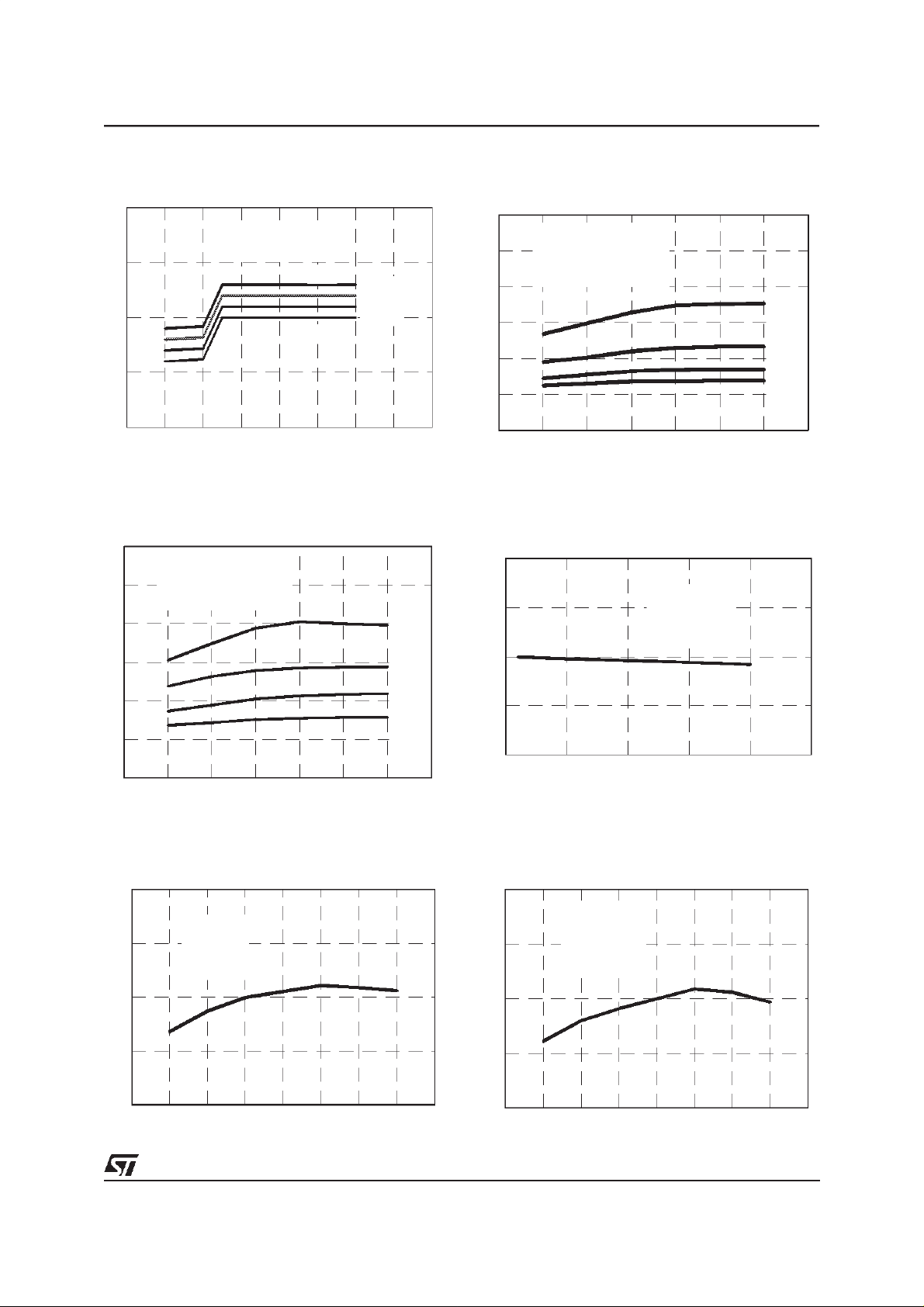
Figure 1. Quiescentcurrentvs. input voltage.
Iq [mA]
30
20
8
6
4
0.2
0.15
0.1
0.05
0
04 8
4/22
V14 = 0, Pin2 = open
Tj = 25°C
12 16 20 24
Vcc [V]
28
Figure2. Quiescent current vs.input voltage
(afterdisable).
Iq [µA]
350
300
250
200
150
100
50
0
0 4 8 12162024
Vcc [V]
V14 = Vref
Tj = 25 °C
L5993
Figure 3. Quiescentcurrentvs. input voltage.
Iq [ mA]
9.0
V14= 0, V5 = Vref
8.5
8.0
7.5
7.0
8 1012141618202224
Rt = 4 .5Kohm,T j = 25°C
1Mhz
100Khz
Vcc [V]
500Khz
300Khz
Figure 5. Quiescentcurrentvs. input voltage
and switchingfrequency.
Iq [mA]
36
Co = 1nF, Tj = 2 5°C
30
24
18
12
DC = 1 00%
1MHz
500KHz
300KHz
100KHz
Figure4. Quiescentcurrent vs. input voltage
and switchingfrequency.
Iq [m A]
36
30
24
18
12
6
0
8 10121416182022
C o = 1nF, T j = 25 °C
DC = 0%
1M Hz
50 0KH z
30 0KH z
100KHz
Vcc [V]
Figure6. Reference voltage vs. load current.
Vref [V]
5.1
5.05
5
4.95
Vcc=15V
Tj= 25°C
6
0
8 10121416182022
Vcc [V]
Figure 7. Vref vs. junctiontemperature.
Vref [V])
5.1
5.05
5
4.95
4.9
-50 -25 0 25 50 75 100 125 150
Vcc = 15V
Iref = 1mA
Tj (°C)
4.9
0 5 10 15 20 25
Iref [mA]
Figure8. Vref vs. junction temperature.
Vref [V]
5.1
Vcc = 15V
5.05
5
4.95
4.9
-50 -25 0 25 50 75 100 125 150
Iref= 20mA
Tj (°C)
5/22
L5993
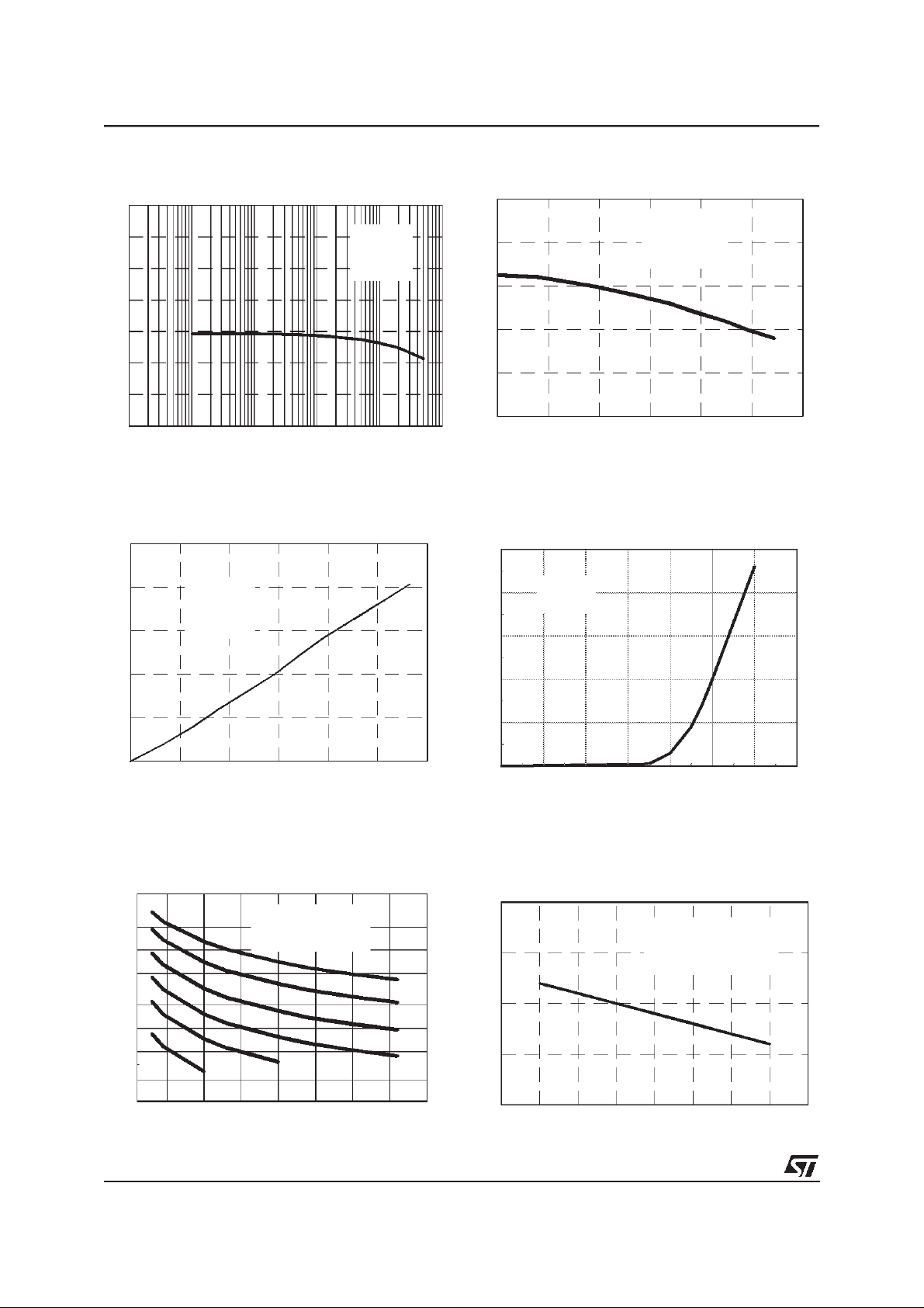
Figure 9. Vref SVRR vs. switchingfrequency.
SVRR (dB)
120
80
40
0
1 10 100 1000 10000
fsw (Hz)
Vcc=15V
Vp-p=1V
Figure 11. Output saturation.
Vsat = V [V]
2.5
2
1.5
10
Vcc = Vc = 15V
Tj = 25°C
Figure10. Output saturation.
Vsat = V [V]
16
14
12
10
8
6
0 0.2 0.4 0.6 0.8 1 1.2
10
Vcc = Vc = 15V
Tj = 25°C
Isource [A]
Figure12. UVLO Saturation
Ipin10 [mA]
50
40
30
Vcc < Vccon
beforeturn-on
1
0.5
0
0 0.2 0.4 0.6 0.8 1 1.2
Isink [A]
Figure 13. Timing resistorvs. switching fre-
quency.
fsw (KHz)
5000
2000
1000
500
200
100
50
20
10
5.6nF
10 20 30 40
Vcc = 15V, V15 =0V
Tj = 25°C
2.2nF
Rt (kohm)
100pF
220pF
470pF
1nF
20
10
0
0 200 400 600 800 1,000 1,200 1,400
Vpin10 [mV]
Figure14. Switchingfrequencyvs. tempera-
ture
fsw (KHz)
320
Rt= 4.5Kohm, Ct = 1nF
310
300
290
280
-50 -25 0 25 50 75 100 125 150
Vcc = 15V,V15=Vref
Tj (°C)
6/22
L5993
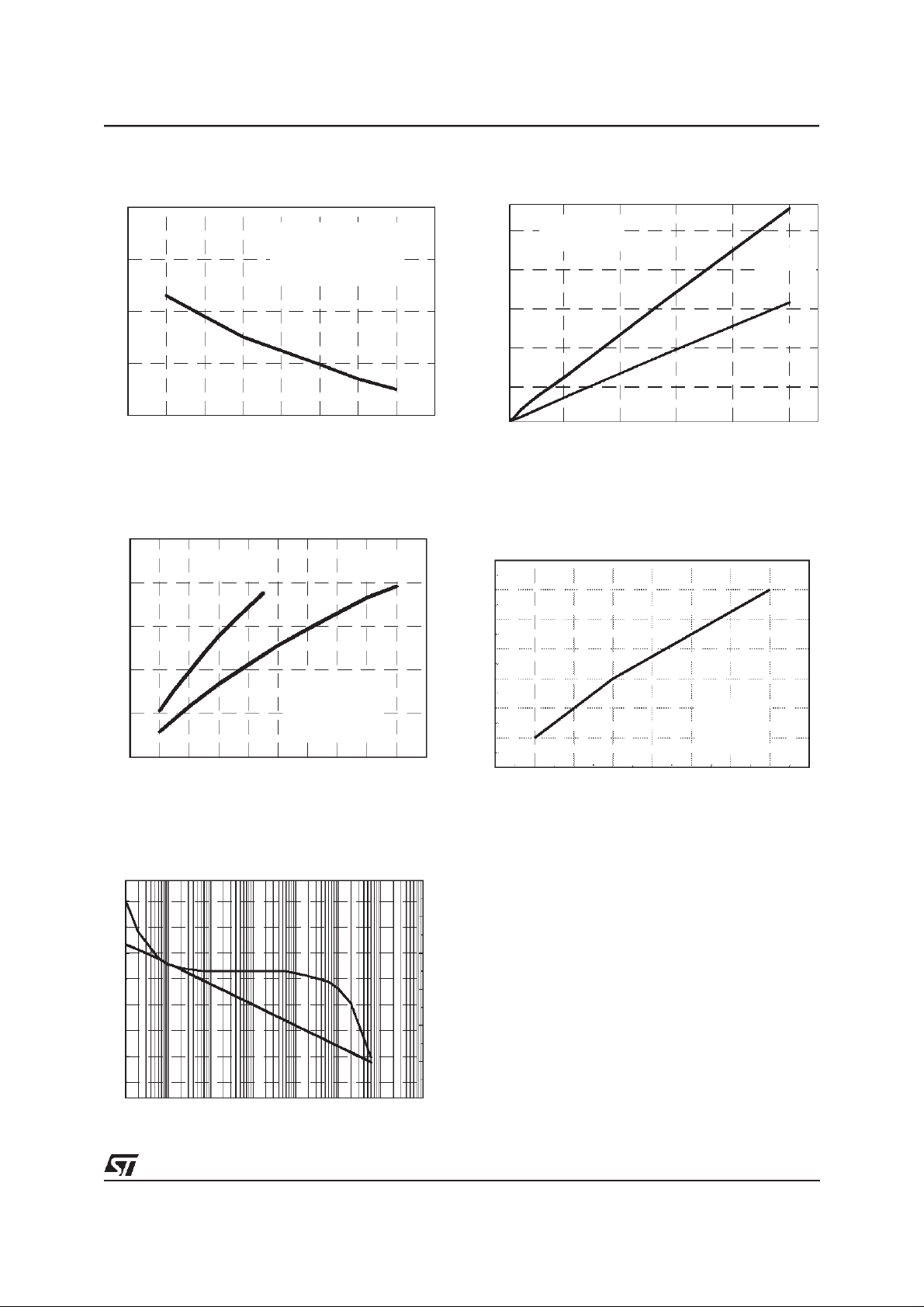
Figure15.Switchingfrequencyvs.temperature.
fsw (KHz)
320
Rt= 4.5Kohm, Ct = 1nF
310
300
290
280
-50 -25 0 25 50 75 100 125 150
Vcc = 15V,V15= 0
Tj (°C)
Figure 17. Maximum Duty Cycle vs Vpin3.
DC Control Voltage Vpin3 [V]
3.5
V15 = Vref
3
V15 = 0V
Figure16. Dead time vs Ct.
Deadtime [ns]
1,500
1,200
900
600
300
Rt =4.5Kohm
V15= 0V
V15= Vref
246810
TimingcapacitorCt [nF]
Figure18. Delay to output vs junctiontem-
perature.
Delay to output (ns)
42
40
2.5
2
Rt = 4.5Kohm,
1.5
Ct = 1nF
1
0 102030405060708090100
Duty Cycle [%]
Figure 19. E/A frequency response.
G [dB]
150
100
50
0
Phase
140
120
100
80
60
40
38
36
34
32
30
28
-50 -25 0 25 50 75 100 125 150
Tj (°C)
PIN10 = OPEN
1V pulse
on PIN13
0.01 0.1 1 10 100 1000 10000 100000
20
f(KHz)
7/22

L5993
CONSTANTPOWER FUNCTION
Pulse-by-pulse current limitation prevents peak
primary current from exceeding a given level.
This, in turn, limits the maximum power deliverable to the output or, in other words, the power
capability of a converter.The capability, however,
depends on switching frequency: for example, in
a discontinuouscurrentmodeflybackthey are just
proportional.
In SMPS’ of raster-scanned CRT displays the
switchingfrequency is usuallysynchronizedtothe
raster line scan signal of the displayin order to increase noise immunity. More and more often,
CRT displays are required to operate within a
range of different video frequencies (e.g. from 31
kHz to 64 kHz), thus also the switching frequency
of the SMPS will vary in thatrange.
In case of some failure,the power throughputmay
be excessive without necessarily tripping the
pulse-by-pulsecurrentlimitationcircuit because of
a highoperating frequency.
For the sake of safety, it would be then desirable
to design the power stage of a converter (power
MOSFET, transformer, catch diode) so as to be
able to withstand the maximum power throughput
under failure conditions. However, this is a considerableincreaseof size and cost.
The ”Constant Power” function of the L5993 allows to overcome this problem. The device
changes the threshold of its pulse-by-pulse current limitation circuit so as to maintain fairly constant the power capability of a flyback converter
despitethe changesof the switching frequency.
This is accomplished by clamping the output of
the error amplifier (VCOMP) to a value which decreases as thefrequency of thesignal fed into pin
1 (SYNC)builds up.
The frequency-to-voltage conversion needed to
achieve this functionality is performed by detecting the peak voltage of the (synchronized) oscillator with a peak-holding circuit. One external capacitoronly is required.
It is important to point out that shape, amplitude
and duration of the synchronization pulses are of
no concernwith this technique.
Figure 20. Sinchronizingthe L5993.
APPLICATION INFORMATION
DetailedPinFunctions Description
Pin 1. SYNC (In/Out Synchronization). This func-
tion allows the IC’soscillator either to synchronize
other controllers (master)or to be synchronizedto
an external frequency (slave).
As a master, the pin delivers positive pulses during the falling edge of the oscillator(see pin 2). In
slave operation the circuit isedge triggered.Refer
to fig. 21 to see how it works. When several IC
work in parallel no master-slave designation is
needed because the fastest one becomes automaticallythemaster.
During the ramp-up of the oscillator the pin is
pulled low by a 600µA internal sink current generator. During the falling edge, that is when the
pulse is released, the 600µA pull-down is disconnected. The pin becomes a generator whose
source capability is typically 7mA (with a voltage
still higher than 3.5V).
In fig. 20, some practical examples of synchronizing the L5993are given.
Pin 2. RCT (Oscillator). A resistor (R
pacitor(C
operatingfrequencyf
C
is charged through RTuntilits voltage reaches
T
), connected as shown in fig. 21 setthe
T
ofthe oscillator.
osc
) and a ca-
T
3V, then is quickly internally discharged. As the
voltage has dropped to 1V it starts being charged
again.
The frequency can be established with the aid of
fig. 13 diagrams or considering the approximate
relationship:
1
⋅ (0.693⋅ RT+ K
=
VREF
15
=
GND/OPEN
15
(1)
T)
2)
(
whereK
≅
f
osc
C
T
isdefinedas:
T
90, V
=
K
T
160 V
and is linked to the duration of the falling edge of
the sawtooth:
T
≅ 30 ⋅ 10-9+KT⋅CT(3)
d
T
is also the duration of the sync pulses deliv-
d
1
L5993 L5993
VREF
4
2
R
T
C
T
(a) (b) (c)
8/22
R
T
L5993
(MASTER)
D97IN766B
4
VREF
12
SYNC
SYNC
L4981A
(SLAVE)
16
R
OSC
17 18
C
OSC
SYNCSYNC
R
OSC
L4981A
(MASTER)
16
1817
C
OSC
1
2
RCTRCT
L5993
(SLAVE)
1
VREFSYNC
4
2
RCT
R
T
C
T
RCT
C
T

Figure 21. Oscillatorand synchronization internalschematic.
4
V
REF
L5993
SYNC
1
R1
CLAMP
R
T
RCT
2
D1
C
T
50Ω
R2R3
+
-
ered at pin 1 and definesthe upper extreme of the
duty cycle range, D
(see pin 15 for Dxdefinition
x
and calculation).
In case V
is connected to VREF, however, the
15
switching frequency of the system will be a half
.
f
osc
If the IC is to be synchronizedto an externaloscillator, R
and CTshould be selected for a f
T
osc
lower than the master frequency in any condition
(typically, 10-20% ), depending on the tolerance
and CT.
of R
T
600µA
D97IN500B
Figure22. Duty cycle control.
V
4
REF
R1
DC
R2
R
T
3µA
3
D
R
CLK
Q
23K
28K
Pin 3.
DC (Duty Cycle Control). By biasing this
pin with a voltage between1 and 3 V it is possible
to set the maximum duty cyclebetween 0 and the
upper extremeD
If D
is the desired maximum duty cycle, the
max
(see pin 15).
x
voltageV3 to be applied to pin 3 is:
(2-Dmax)
=5-2
V
3
is determined by internal comparison be-
D
max
(4)
tween V3 and the oscillator ramp (see fig. 22),
thus in case the device is synchronized to an external frequency f
(and therefore the oscillator
ext
amplitudeis reduced),(4) changes into:
= 5 − 4 ⋅ exp
V
3
−
RT⋅ CT⋅ f
max
ext
(5)
D
A voltage below 1V will inhibit the driver output
stage. This could be used for a not-latcheddevice
disable, for example in case of overvoltage protection(see applicationideas).
If no limitation on the maximum duty cycle is re-
TO PWM LOGIC
+
2
-
D97IN711A
), the pin has to be left float-
C
T
quired (i.e. D
RCT
MAX=DX
ing. An internal pull-up (see fig. 22) holds the voltage above 3V. Should the pin pick up noise (e.g.
during ESD tests), it can be connected to VREF
througha 4.7kΩresistor.
Pin 4. VREF (Reference Voltage). The device is
provided with an accurate voltage reference
(5V±1.5%)able to deliver some mA to an external
circuit.
A small film capacitor (0.1µF typ.), connected
between this pin and SGND, is recommended to
ensure the stability of the generator and to prevent
noisefromaffectingthereference.
Before device turn-on, this pin has a sink current
capabilityof 0.5mA.
9/22

L5993
Pin 5.
VFB (Error Amplifier Inverting Input). The
feedbacksignal is applied to this pin and is compared to the E/A internal reference (2.5V). The
E/A output generates the control voltage which
fixes the duty cycle.
The E/A features high gain-bandwidth product,
which allows to broaden the bandwidth of the
overall controlloop,high slew-rateand current capability, which improves its large signal behavior.
Usually the compensation network, which stabilizes the overall control loop, is connected between this pin andCOMP (pin 6).
Pin 6.
COMP (Error Amplifier Output). Usually,
this pin is used for frequency compensation and
the relevant network is connected between this
pin and VFB (pin 5). Compensation networks towards ground are not possible since the L5993
E/A is a voltage mode amplifier (low output impedance). See application ideas for some example ofcompensationtechniques.
Pin 7. SS (Soft-Start). At device start-up, a capacitor (Css) connected between this pin and
SGND (pin 12) is charged by an internal current
generator, ISSC, up to about 7V. During this
ramp, the E/A output is clamped by the voltage
across Cssitself and allowed to rise linearly, starting from zero, up to the steady-state value imposed by the control loop. The maximum time interval during which the E/A is clamped,referredto
as soft-starttime, is approximately:
T
where R
sense
13) and I
through R
3⋅R
≅
ss
is the currentsense resistor (see pin
is the switch peak current (flowing
Qpk
), which depends on the output
sense
sense
I
SSC
⋅
I
Qpk
⋅ C
ss
(6)
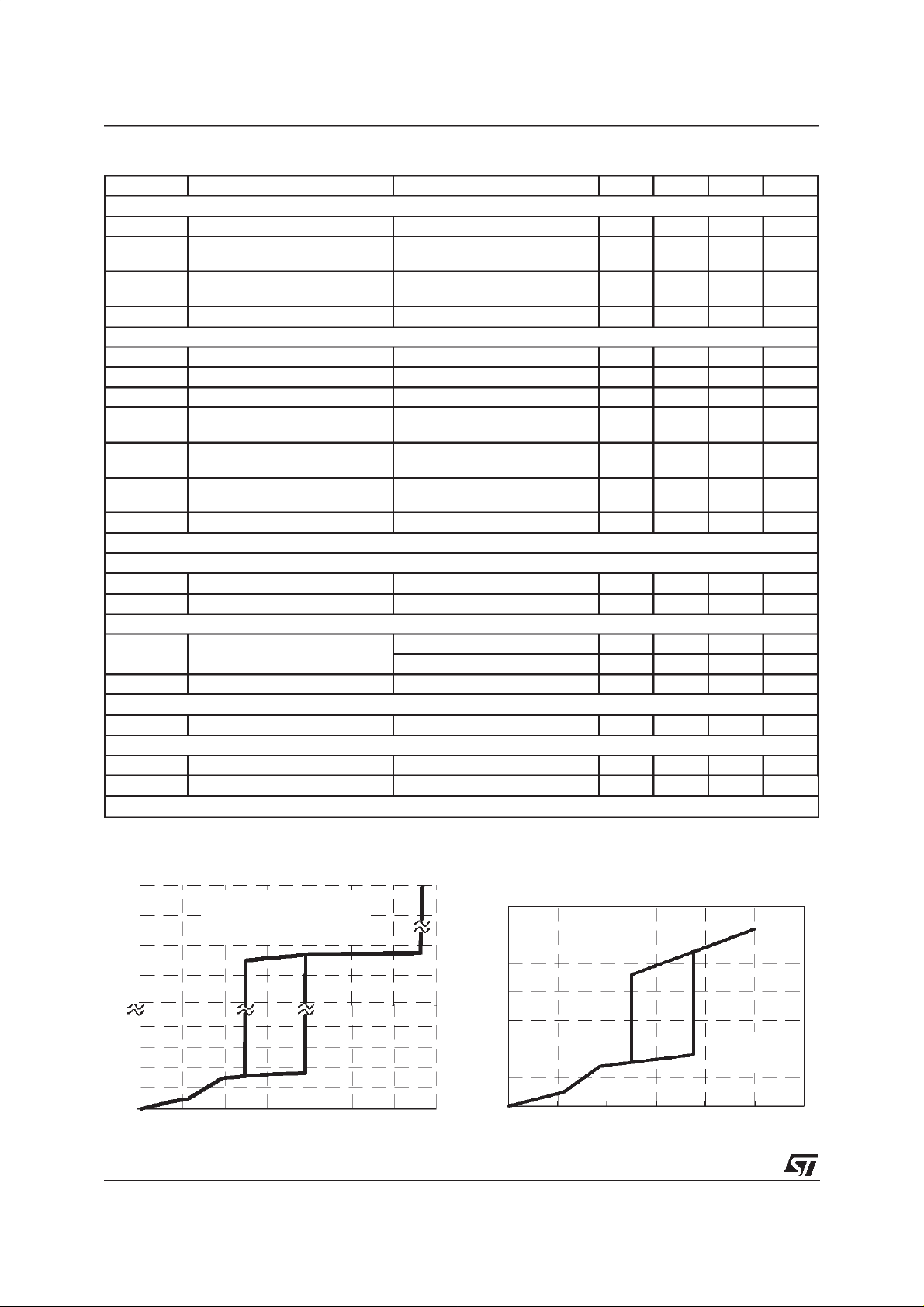
Figure 24. Hiccup mode operation.
Figure23. Regulation characteristicandre-
latedquantities
V
OUT
D.C.M. C.C.M.
T
ON
D97IN495
load. Usually, C
A
B
D
I
SHORTIOUT(max)
is selected for a TSSin the or-
SS
I
Qpk
1-2 ·I
Qpk
I
Qpk(max)
C
T
ON(min)
I
OUT
der ofmilliseconds.
As mentioned before, the soft-start intervenes
also in case of severe overload or short circuit on
the output. Referring to fig. 23, pulse-by-pulse
current limitation is somehow effective as long as
the ON-time of the power switch can be reduced
(from A to B). After the minimum ON-time is
reached (from B onwards) the current is out of
control.
To prevent this risk, a comparator trips an overcurrent handling procedure, named ’hiccup’ mode
operation,when a voltage above 1.2V (point C) is
detected on current sense input (ISEN, pin 13).
Basically,the IC is turned off and then soft-started
as long as the faultcondition is detected.As a result, the operating point is moved abruptly to D,
creating a foldback effect. Fig. 24 illustrates the
operation.
The oscillation frequency appearing on the soft-
10/22
I
OUT
I
SEN
FAULT
SS
5V
0.5V
SHORT
7V
T
hic
D98IN986
time

L5993
start capacitorin case of permanent fault, referred
to as ’hiccup” period, is approximatelygiven by:
T
hic
≅ 4.5 ⋅
I
SSC
+
I
SSD
⋅ C
(7)
ss
1
1
Since the system tries restarting each hiccup cycle, there is not any latchoffrisk.
”Hiccup” keeps the system in control in case of
short circuits but does not eliminate power components overstress during pulse-by-pulse limitation (from A to C). Other external protection circuits are needed if a better control of overloadsis
required.
Pin 8. VCC (Controller Supply). This pin supplies
the signal part of the IC. The device is enabled as
VCC voltage exceeds the start threshold and
works as long as the voltage is above the UVLO
threshold. Otherwise the device is shut down and
the current consumption is extremely low
(<150µA). This is particularly useful for reducing
the consumption of the start-upcircuit (in thesimplest case, just one resistor), which is one of the
most significant contributions to power losses
when a converter is lightly loaded.
An internal Zener limits the voltage on VCC to
25V. The IC current consumption increases considerablyif this limit is exceeded.
A smallfilmcapacitor between this pin and SGND
(pin 12), placed as close as possible to the IC, is
recommendedtofilter high frequencynoise.
Pin 9.
VC (Supply of thePower Stage). It supplies
the driver of the external switch and therefore absorbs a pulsedcurrent. Thus it is recommendedto
place a buffer capacitor (towards PGND, pin 11,
as close as possible to the IC) able to sustain
these current pulses and in order to avoid them
inducingdisturbances.
This pin can be connectedto the buffer capacitor
directly or through a resistor, as shown in fig. 25,
to control separately the turn-on and turn-off
speed of the external switch, typically a PowerMOS. At turn-onthe gate resistance is R
turn-off is R
Pin 10.
only.
g
OUT (Driver Output). This pin is the out-
g+Rg’,
at
put of the driver stage of the external power
switch. Usually, this will be a PowerMOS, although the driver is powerful enough to drive
BJT’s(1.6A source,2A sink, peak).
The driver is made up of a totempole with a highside NPN Darlington and a low-side VDMOS, thus
there is no need of an external diode clamp to
prevent voltage from going below ground. An internal clamp limits the voltage delivered to the
gate at 13V. Thus it is possible to supply the
driver (Pin 9) with higher voltageswithout any risk
Figure25. Turn-on and turn-offspeedsadjust-
ment
Rg’
PGND
V
C
9
10
OUT
Rg
11
Rg(ON)=Rg+Rg’
Rg(OFF)=Rg
V
CC
DRIVE
CONTROL
L5993
D97IN767
8
13V
&
Figure26. Pull-Downof the output in UVLO
OUT
10
V
REFOK
12
SGND
D97IN538
of damagefor thegate oxide of the external MOS.
The clamp does not cause any additional increase of power dissipation inside the chip since
the current peak of the gate charge occurs when
the gate voltage is few volts and the clamp is not
active. Besides, no current flows when the gate
voltageis 13V, steady state.
Under UVLO conditions an internal circuit (shown
in fig.26) holds the pin low in order to ensure that
the external MOS cannot be turned on accidentally. The peculiarity of this circuit is its ability to
mantain the same sink capability (typically, 20mA
@ 1V) from V
= 0V up to the start-up threshold.
CC
When the threshold is exceeded and the L5993
starts operating,V
is pulled high (refer to fig.
REFOK
26) andthe circuit is disabled.
It is then possible to omit the ”bleeder” resistor
(connected between the gate and the source of
the MOS) ordinarily used to prevent undesired
switching-on of the external MOS because of
someleakagecurrent.
Pin 11.
PGND (Power Ground). The current loop
during the discharge of the gate of the external
MOS is closed through this pin. This loop should
be as short as possible to reduce EMI and run
separatelyfrom signal currentsreturn.
11/22

L5993
Figure 27. Internal LEB.
I
3V
0
CLK
13
ISEN
FROM E/A
+
OVERCURRENT
1.2V
COMPARATOR
Pin 12. SGND(Signal Ground). This ground references the control circuitry of the IC, so all the
ground connections of the external parts related
to control functionsmust lead to this pin. In laying
out the PCB, care must be taken in preventing
switched high currents from flowing through the
SGND path.
Pin 13.
ISEN (Current Sense). This pin is to be
connected to the ”hot” lead of the current sense
resistor R
(being the other one grounded),to
sense
get a voltage ramp which is an image of the current of the switch (I
). When this voltage is equal
Q
to:
2V
+
-
PWM
COMPARATOR
+
-
D97IN503
Figure28. Disable (Latched)
DISABLE
SIGNAL
DIS
14
C
2.5V
TO
PWM
LOGIC
TO FAULT
LOGIC
+
-
D
R
UVLO
Q
DISABLE
D97IN502
V
13pk
=
⋅
I
R
Qpk
sense
V
=
COMP
− 1.4
3
(8)
the conductionof theswitch is terminated.
To increase the noise immunity, a ”Leading Edge
Blanking” of about 100ns is internally realized as
shown in fig. 27. Because of that, the smoothing
RC filter between this pin and R
sense
could be re-
movedor, at least, considerably reduced.
Pin 14.
DIS (Device Disable). When the voltage
on pin 14 rises above 2.5V the IC is shut down
and it is necessaryto pull VCC (IC supply voltage,
pin 8) below the UVLO threshold to allow the device to restart.
The pin can be driven by an external logic signal
in case of power management, as shown in fig.
28. It is also possible to realize an overvoltage
protection, as shown in the section ” Application
Ideas”.Ifused, bypass this pin to ground with a filter capacitor to avoid spurious activation due to
noise spikes. If not, it must be connected to
SGND.
Pin 15. DC-LIM (Maximum Duty Cycle Limit).The
upper extreme, Dx, of the duty cycle range depends on the voltage applied to this pin. Approxi-
mately,
R
T
D
x
≅
RT+ 230
(
9)
if DC-LIM is grounded or left floating. Instead,
connecting DC-LIM to VREF (half duty cycle option),Dx will be set approximately to:
R
≅
D
x
T
2 ⋅ RT+ 260
(10)
and the output switching frequency will be halved
with respect to the oscillator one because an internal T flip-flop (see block diagram, fig. 1) is activated.Fig. 29 shows the operation.
The half duty cycle option speeds up the discharge of the timing capacitor C
(in order to get
T
duty cycles as close as possible to 50%) so the
oscillator frequency - with the same R
and CT-
T
will be slightly higher.
The halving of frequencycan be used to reduce
losses at light load in all those systems that must
comply with requirements regarding energy consumption (e.g. monitor displays, see ”Application
Ideas”).
12/22

Figure 29. Half duty cycle option.
V15=GND
V5=V13=GND
L5993
t
d
V2
t
c
=
D
X
tc+t
d
t
c
V15=VREF
V5=V13=GND
t
c
t
d
D97IN498
Figure 30. Constant Power circuit internal schematic
VREF
R
T
C-POWER 16
C
CP
RCT
C
T
VFB
5
2.5V
4
2
E/A
+
CLAMP
-
+
BUFFER
COMP
6
D2
Q2
Q1
D1
47KΩ
D97IN768A
V10
V2
V10
30KΩ
30KΩ
15KΩ
1V
TIMING
113
SYNC ISEN
t
c
D
=
X
2·tc+t
d
-
+
COMPARATOR
PWM
L5993
TO PWM
LATCH
Pin 16. C-POWER (Constant Power Function).
An external capacitor connectedbetween this pin
and SGND completes the peak-holdingcircuitthat
detects the peak voltage of the synchronized oscillator. The circuit gets a DC voltage (which decreases as the synchronizing frequency fed into
pin 1 (SYNC)rises) used to clampthe error amplifier output(V
), as shown in thedetailedinter-
COMP
nal schematicof fig.30.
In this way the pulse-by-pulse setpoint is moved
downwardsas thefrequenc yrises(andviceversafor
a frequencydecrease,dueto the47kΩ dischargeresistor) and, as a result, the maxim umpower deliverableto theloadisheldroughlyconstant .
The external capacitor must be large enough to
get a real DC voltage on the pin. Considering the
spread of the internal 47kΩ resistor, the minimum
capacitancevalue(C
) neededto have less than
CP
1% ripplesuperimposedon the DC voltage is:
>
330 ⋅ƒ
1
,
min
C
CP
where ƒ
(Hz)is the minimumsynchronizingfre-
min
quency.
When this function is not used, pin 16 has to be
connecteddirectly to pin 4.
Considering the ordinary design criteria for the
transformer, the circuit usually works well without
any adjustment. Anyway, the variations of the
maximumpower limiton varying the switching frequency and/or the mains voltage can be minimized by modifying one or more of the following
parameters:
- Primaryinductance;
- Transformerturnsratio;
- Oscillatorfree-running frequency;
- Senseresistor.
A trial process is required, involving the parame-
ters that are more practicable to modify. In fact,
the optimum behavior is achieved for a specific
combination of the above parameters and de-
13/22

L5993
pends both on the mains voltage range and the
synchronizationfrequencyrange.
An additional ”fine tuning” can be achieved by
adding a small DC offset (in the ten mV) on the
current sense pin (13, ISEN).
For wide range mains applications it is anyway
recommendedtocompensatethe propagationdelay of the currentsense path (PWMcomparator +
latch + driver) with the circuit shown in the ”Application Ideas”section, fig. 41.
Layout hints
Generally speaking a proper circuitboardlayout is
vital for correct operationbut is not an easy task.
Careful component placing, correct traces routing,
appropriate traces widths and, in case of high
voltages, compliance with isolation distances are
the major issues. The L5993 eases this task by
putting two pins at disposal for separate current
returns of bias (SGND) and switch drive currents
(PGND) The matter is complex and only few important points will be here reminded.
1) All current returns (signal ground, power
ground, shielding, etc.) should be routed sepa-
rately and should be connected only at a single
ground point.
2) Noise coupling can be reduced by minimizing
the area circumscribed by current loops. This
applies particularly to loops where high pulsed
currentsflow.
3) For high current paths, the traces should be
doubled on theother side of the PCB whenever
possible: this will reduce both the resistance
and the inductanceof the wiring.
4) Magnetic field radiation (and stray inductance)
can be reduced by keeping all traces carrying
switchedcurrentsas shortas possible.
5) In general, traces carrying signal currents
should run far from traces carrying pulsed currents or with quickly swinging voltages. From
this viewpoint, particular care should be taken
of the high impedancepoints (current sense input, feedback input, ...). It could be a good idea
to route signal traces on one PCB side and
power traceson theother side.
6) Provide adequate filtering of some crucial
points of thecircuit,such as voltage references,
IC’s supply pins, etc.
14/22

L5993
APPLICATIONIDEAS
Here followsa seriesof ideas/suggestionsaimedat
either improving performance or solving common
application problems of L5993 based supplies.
Figure 31. Typical applicationcircuitfor 15” Multisyncmonitor(70W)
80V
50V
C62
C52
D53
D52
18
16
17
F
10µ
100µF 100V
100V
C53
R51
GND
C54
151314
Q71
220µF 100V
D54
6.3V
C71
C55
HEATER
CONTROL
R72
R71
F
16V
470µ
D55
Q72
C56
OFF
470µF 25V
14V
NOR SUSPEND
C57
470µF 25V
111210
14V
SWITCHED
UNSWITCHED
C74 R75
Q73
47
R52
C58
D56
R53
R73
47µF 25V
4.7K
16V
ZD71
16V
+50V
-12V
C59
10K
VR51
Q75
SWITCHED
100
R56
0.01µF
R55
18K
C61
DEF.
H/V
R74
0.022µF
CONTROL
SUSPEND OFF
Q74
R58
1.2K
NOR
C11 4700pF 4KV C12
R19 4.7M R20 4.7M
BD01
F01 AC 250V T3.15A
1
R01 2.2
LF01
C02
C01
P1
200V
D05
R03 10K
387D02 1N4148
-1000
BYW13
Q01
KSP45
R04
D04 RGP100
470K
Q02
KTC1815Y
R07 47
20V
ZD01
R12 33KR13 5.1K
R05
10K
Q01
STP6
NA60FI
R08 2213R11 1K
C04 470µF
R06 27
91415
C07 1µF
R09 5.6K
8
10
5
2
4
10K
R05
C06 5600pF
F
C10
0.1µ
R18
22K
R02
220K
F
400V
C03 220µ
0.1µF
0.1µF
AC IM
C05
L5993
1
R17 1K
SYNC IN
R54
R10
470pF
12
1K
0.22
5.6V
ZD02
PC01
R21 470
C08
6
11
16
7
C09 0.01µF
470pF
C11
Q51
TL431
D97IN619A
1µF
15/22

L5993
Figure 32. Isolated MOSFETDrive& Current TransformerSensingin 2-switchTopologies
V
IN
V
C
9
10
L5993
13
1112
PGND
SGND
Figure 33. Low consumptionstart-up
OUT
ISEN
ISOLATION
BOUNDARY
D97IN769
2.2MΩ 33KΩ
20V
47KΩ
D97IN770B
Figure 34. BipolarTransistorDrive
V
IN
STD1NB50-1
V
CC
V
REF
4
8
L5993
T
SELF-SUPPLY
WINDING
12 11
V
IN
V
CC
8
V
C
9
OUT
10
16/22
L5993
ISEN
13
11
PGND
D97IN771

Figure 35. Typical E/A compensationnetworks.
L5993
From V
O
R
i
C
R
d
f
COMP
Error Amp compensation circuit for stabilizing any current-mode topology
for boost and flyback converters operating with continuous inductor current.
From V
O
R
P
R
i
C
P
C
R
d
f
COMP
Error Amp compensation circuit for stabilizing current-mode boost and
topologies operating with continuous inductor current.
Figure 36. Feedback with optocoupler
VFB
R
VFB
R
2.5V
+
1.3mA
+
5
EA
f
6
2R
R
12
SGND
except
2.5V
+
5
f
6
+
1.3mA
2R
EA
R
12
D97IN507
SGND
flyback
V
OUT
COMP
6
L5993
5
VFB
Figure 37. Slope compensation techniques
V
REF
4
R
T
RCT
2
C
R
I
R
SLOPE
SENSE
T
ISEN
OPTIONAL
13
L5993
12
SGND
I
R
SLOPE
R
SENSE
R
T
OPTIONAL
V
REF
RCT
C
T
ISEN
TL431
D97IN772
4
2
L5993
13
12
SGND
SGND
D97IN773A
L5993
12
10
13
OPTIONAL
OUT
ISEN
RR
R
SLOPE
C
R
SLOPE
SENSE
17/22

L5993
Figure 38. Protection against overvoltage/feedbackdisconnection(latched)
R
DIS
START
V
CC
L5993
14
12 11
SGND
V
8
PGND
D97IN774
Z
2.2K
DIS
R
START
V
CC
L5993
14
12 11
SGND
8
PGND
D98IN906
Figure 39. Protection against overvol-
tage/feedbackdisconnection(not
Figure40. Device shutdown on overcurrent
latched)
I
≅
R
1
D97IN776A
pk max
R
2
VREF
DC
R
4
3
START
V
12
CC
8
L5993
11
D97IN775A
PGND
L5993
SGND
14
13
1211
VREF
4
DIS
ISEN
OPTIONAL
Figure 41. Constant power in pulse-by-pulsecurrent limitation(flybackdiscontinuous)
V
IN
80 ÷ 400V
PGND
DC
OUT
L5993
SGND
R
10
ISEN
13
1211
L
p
FF
R·L
p
RFF= 6·10
R
R
SENSE
6
R
SENSE
R
R
SENSE
2.5
SENSE
I
R
2
1-
•
R
1
I
pk
Figure 42. Voltage mode operation.
18/22
10K
COMP
DC
3
L5993
6
12 13
SGND ISEN
D97IN777
D97IN778A

Figure 43. Device shutdown on mainsundervoltage.
V
IN
80÷400V
DC
R1
4.7K
10KΩR25.1
Figure 44. Constant power ”Fine Tuning”.
VREF
SGND PGND
D97IN779A
4
3
12 11
L5993
L5993
SGND
VREF ISEN
D97IN780A
L5993
12
413
R
10
A
R
OPTIONAL
R
SENSE
Figure 45. Synchronizationto flyback pulses (for monitors).
SYNC
1KΩ
5.1V
SGND
L59931
12
D97IN781A
Figure 46. Switching frequency halving on absence of sync.signal(for monitor).
1KΩ
5.1V
V
REF
4
R1
f
D97IN782A
CR2
DC-LIM
L5993
15
1
SYNC
12
(R
1
//R2)•C>>
SGND
1
f
min
19/22

L5993
DIM.
MIN. TYP. MAX. MIN. TYP. MAX.
a1 0.51 0.020
B 0.77 1.65 0.030 0.065
b 0.5 0.020
b1 0.25 0.010
D 20 0.787
E 8.5 0.335
e 2.54 0.100
e3 17.78 0.700
F 7.1 0.280
I 5.1 0.201
L 3.3 0.130
Z 1.27 0.050
mm inch
OUTLINE AND
MECHANICAL DATA
DIP16
20/22

L5993
DIM.
MIN. TYP. MAX. MIN. TYP. MAX.
A 1.75 0.069
a1 0.1 0.25 0.004
a2 1.6 0.063
b 0.35 0.46 0.014 0.018
b1 0.19 0.25 0.007 0.010
C 0.5 0.020
c1 45°(typ.)
D (1) 9.8 10 0.386 0.394
E 5.8 6.2 0.228 0.244
e 1.27 0.050
e3 8.89 0.350
F (1) 3.8 4 0.150 0.157
G 4.6 5.3 0.181 0.209
L 0.4 1.27 0.016 0.050
M 0.62 0.024
S
mm inch
0.009
8°(max.)
OUTLINE AND
MECHANICAL DATA
SO16 Narrow
(1) D andF do notinclude moldflash or protrusions. Moldflash or potrusionsshall not exceed 0.15mm (.006inch).
21/22

L5993
Information furnished is believed tobe accurate and reliable. However, STMicroelectronics assumes no responsibility for the consequences
of use of such information nor for any infringement of patents or other rights of third parties which may result from its use. No license is
granted by implication or otherwise under any patent or patent rights of STMicroelectronics. Specification mentioned in this publication are
subject to change without notice. This publication supersedes and replaces all information previously supplied. STMicroelectronics products
are not authorized for use as critical components in life support devices or systems without express written approval of STMicroelectronics.
The ST logo is a registered trademark of STMicroelectronics
1999 STMicroelectronics – Printed in Italy – All Rights Reserved
STMicroelectronics GROUP OF COMPANIES
Australia - Brazil - China - Finland - France - Germany - Hong Kong - India - Italy - Japan - Malaysia - Malta - Morocco -
Singapore - Spain - Sweden - Switzerland - United Kingdom - U.S.A.
http://www.st.com
22/22
 Loading...