

L5991
PRIMARY CONTROLLER WITH STANDBY
CURRENT-MODE CONTROLPWM
SWITCHINGFREQUENCYUPTO1MHz
LOW START-UP CURRENT (< 120µA)
HIGH-CURRENT OUTPUT DRIVE SUITABLE
FOR POWERMOSFET(1A)
FULLY LATCHED PWM LOGIC WITH DOU-
BLE PULSE SUPPRESSION
PROGRAMMABLEDUTYCYCLE
100%AND50%MAXIMUMDUTY CYCLELIMIT
STANDBYFUNCTION
PROGRAMMABLESOFT START
PRIMARY OVERCURRENT FAULT DETEC-
TION WITH RE-STARTDELAY
PWMUVLO WITH HYSTERESIS
IN/OUTSYNCHRONIZATION
LATCHEDDISABLE
INTERNAL 100ns LEADING EDGE BLANK-
ING OF CURRENT SENSE
PACKAGE:DIP16 ANDSO16
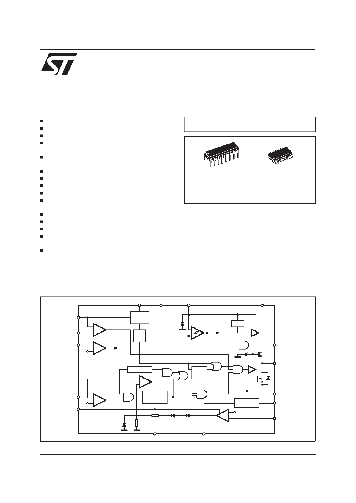
DESCRIPTION
This primary controllerI.C., developed in BCD60II
technology, has been designed to implement off
L5991A
MULTIPOWER BCD TECHNOLOGY
DIP16 SO16
ORDERING NUMBERS:
line or DC-DC power supply applications using a
fixedfrequencycurrentmode control.
Based on a standard current mode PWM controller this device includes some features such as
programmablesoft start, IN/OUT synchronization,
disable (to be usedfor overvoltageprotection and
for power management), precise maximum Duty
Cycle Control, 100ns leading edge blanking on
current sense, pulse by pulse current limit, overcurrent protection with soft start intervention, and
Standbyfunction for oscillatorfrequencyreduction
when the converteris lightlyloaded.
L5991/L5991A (DIP16)
L5991D/L5991AD (SO16)
BLOCK DIAGRAM
RCT
3
DC
14
DIS
2.5V
13
ISEN
1.2V
SS
August 1999
+
-
-
+
OVER CURRENT
+
-
DIS
BLANKING
1V R
SYNC DC-LIM
TIMING2
T
PWM
FAULT
SOFT-START
2R
12
SGND COMP
25V
15V/10V
VREF OK
CLK
DIS
V
CC
Vref
+
PWM UVLO
-
SQ
R
STAND-BY ST-BY
2.5V7
+
E/A
-
6
13V
VREF
VREF
48151
D97IN725A
9
V
C
10
OUT
11
PGND
16
5
VFB
1/23
L5991 - L5991A
ABSOLUTEMAXIMUMRATINGS
Symbol Parameter Value Unit
V
CC Supply Voltage (I
I
OUT
Output Peak Pulse Current 1.5 A
Analog Inputs & Outputs (6,7) -0.3 to 8 V
Analog Inputs & Outputs (1,2,3,4,5,15,14,13, 16) -0.3 to 6 V
P
tot
T
j
T
stg
(*) maximum package power dissipation limits must be observed
Power Dissipation @ T
Junction Temperature, Operating Range -40 to 150 °C
Storage Temperature, Operating Range -55 to 150 °C
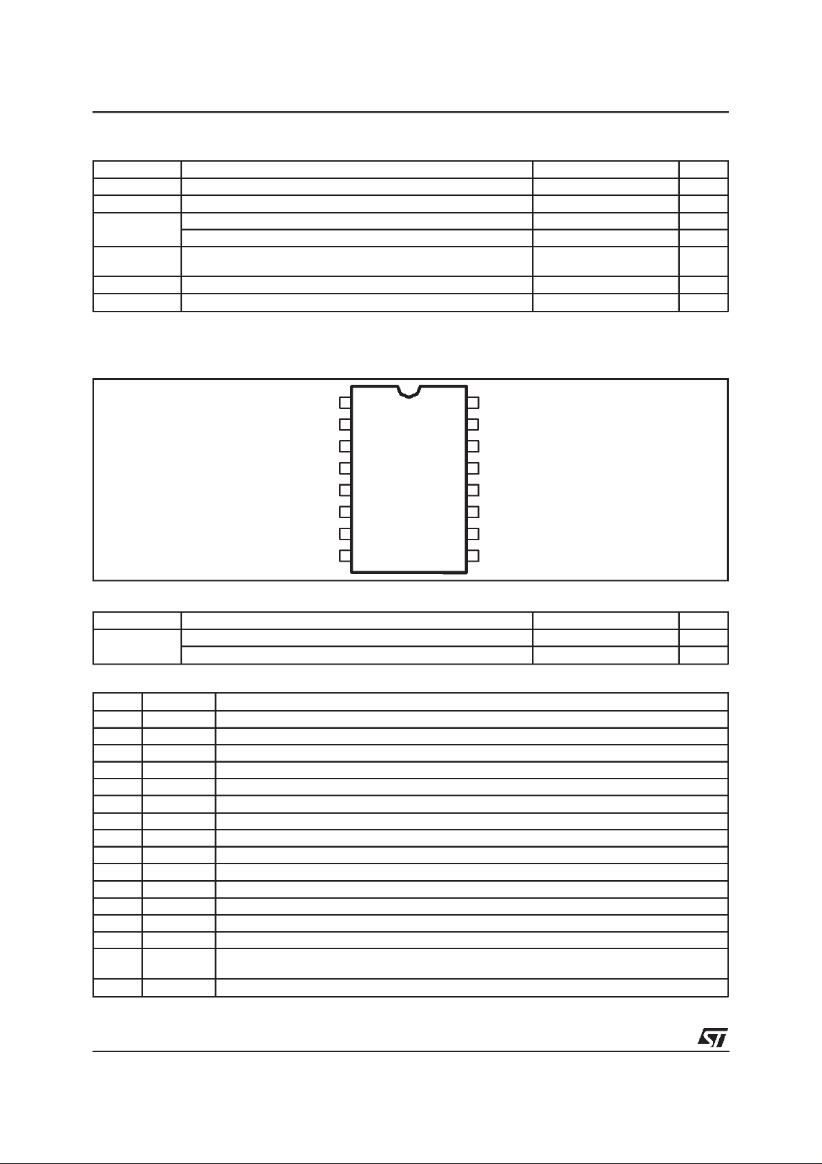
PIN CONNECTION
< 50mA) (*) selflimit V
CC
@T
=70°C (DIP16)
amb
=50°C (SO16)
amb
1
0.83
W
W
SYNC
RCT
DC
VREF
VFB
COMP
SS
V
CC
1
2
3
4
5
6
7 OUT
8V
15
14
13
12
11
10
ST-BY16
DC-LIM
DIS
ISEN
SGND
PGND
9
C
THERMAL DATA
Symbol Parameter Value Unit
R
th j-amb
Thermal Resistance Junction -Ambient (DIP16) 80
Thermal Resistance Junction -Ambient (SO16) 120
PIN FUNCTIONS
N. Name Function
1 SYNC Synchronization. A synchronization pulse terminates the PWM cycle and discharges Ct
2 RCT Oscillator pin for external C
T,RA,RB
3 DC Duty Cycle control
4 VREF 5.0V +/-1.5% reference voltage @ 25°C
5 VFB Error Amplifier Inverting input
6 COMP Error Amplifier Output
7 SS Soft start pin for external capacitor Css
8V
9V
CC Supply for internal ”Signal” circuitry
C
Supply for Power section
10 OUT High current totem pole output
11 PGND Power ground
12 SGND Signal ground
13 ISEN Current sense
14 DIS Disable. It must never be left floating. TIE to SGND if not used.
15 DC-LIM Connecting this pin to Vref, DC is limited to 50%. If it is left floating or grounded no limitation is
imposed
16 ST-BY Standby. Connect a resistor to RCT. Connect to VREF or floating if not used.
components
C/W
°
C/W
°
2/23
L5991 - L5991A
ELECTRICALCHARACTERISTICS
CC
=15V; Tj= 0 to 105°C; RT=13.3kΩ(*)CT= 1nF;
(V
unless otherwisespecified.)
Symbol Parameter Test Condition Min. Typ. Max. Unit
REFERENCE SECTION
V
REF
T
S
I
OS
OSCILLATOR SECTION
ERROR AMPLIFIER SECTION
V
I
G
OPL
SVR Supply Voltage Rejection V
V
OL
V
OH
O Output Source Current VCOMP > 4V, V
I
S
R
PWM CURRENT SENSE SECTION
I
b
I
S
V
t
SOFT START SECTION
I
SSC
I
SSD
V
SSSAT
V
SSCLAMP
LEADING EDGE BLANKING
OUTPUT SECTION
V
OL
V
OH
V
OUT CLAMP
(*) RT=RA//RB,RA=RB= 27kΩ, see Fig. 22.
Output Voltage Tj=25°C; IO= 1mA 4.925 5.0 5.075 V
Line Regulation V
Load Regulation I
= 12 to 20V; Tj=25°C 2.0 10 mV
CC
= 1 to 10mA; Tj=25°C 2.0 10 mV
O
Temperature Stability 0.4 mV/°C
Total Variation Line, Load, Temperature 4.80 5.0 5.130 V
Short Circuit Current Vref = 0V 30 150 mA
Power Down/UVLO V
CC
= 6V; I
Initial Accuracy pin 15 = Vref; T
pin 15 = Vref; V
pin 15 = Vref; V
Duty Cycle pin 3 = 0,7V, pin 15 = V
pin 3 = 0.7V, pin 15 = OPEN
pin 3 = 3.2V, pin 15 = V
pin 3 = 3.2V, pin 15 = OPEN
= 0.5mA 0.2 0.5 V
sink
j
V
comp
= 12 to 20V
CC
V
comp
= 12 to 20V
CC
V
comp
=25°C
= 4.5V
= 4.5V
=2V
REF
95 100 105 kHz
93 100 107 kHz
46.5 50 53.5 kHz
0
0
REF
47
93
Duty Cycle Accuracy pin 3 = 2.79V, pin 15 = OPEN 75 80 85 %
Oscillator Ramp Peak 2.8 3.0 3.2 V
Oscillator Ramp Valley 0.75 0.9 1.05 V
Input Bias Current V
to GND 0.2 3.0 µA
FB
Input Voltage VCOMP =VFB 2.42 2.5 2.58 V
Open Loop Gain V
Output Low Voltage I
Output High Voltage I
Output Sink Current V
= 2to 4V 60 90 dB
COMP
= 12 to 20V 85 dB
CC
= 2mA 1.1 V
sink
= 0.5mA, VFB= 2.3V 5 6 V
source
= 2.3V 0.5 1.3 2.5 mA
FB
COMP = 1.1V,V
= 2.7V 2 6 mA
FB
Unit Gain Bandwidth 1.7 4 MHz
Slew Rate 8 V/µs
Input Bias Current I
Maximum Input Signal V
=0 3 15
sen
= 5V 0.92 1.0 1.08 V
COMP
Delay to Output 70 100 ns
Gain 2.85 3 3.15 V/V
Fault Threshold Voltage 1.1 1.2 1.3 V
SS Charge Current Tj=25°C 142026µA
SS Discharge Current VSS = 0.6V Tj=25°C 5 10 15
SS Saturation Voltage DC = 0% 0.6 V
SS Clamp Voltage 7 V
Internal Masking Time 100 ns
Output Low Voltage IO= 250mA 1.0 V
Output High Voltage IO= 20mA; VCC= 12V 10 10.5 V
= 200mA; VCC = 12V 9 10 V
I
O
Output Clamp Voltage IO= 5mA; VCC = 20V 13 V
Collector Leakage V
CC = 20V VC = 24V 2 20 µA
%
%
%
%
A
µ
A
µ
3/23
L5991 - L5991A
ELECTRICALCHARACTERISTICS
(continued.)
Symbol Parameter Test Condition Min. Typ. Max. Unit
OUTPUT SECTION
Fall Time C
Rise Time C
UVLO Saturation V
O
C
O
O
C
O
CC =V
I
sink
= 1nF
= 2.5nF
= 1nF
= 2.5nF
C
= 10mA
= 0 to V
CCON
20
35
50
70
60 ns
100 ns
1.0 V
SUPPLY SECTION
V
CCON
V
CCOFF
V
Startup voltage L5991
L5991A147.8
Minimum Operating Voltage
L5991
L5991A
hys
UVLOHysteresis L5991
L5991A
I
S
I
op
I
q
V
Z
Start Up Current Before Turn-on at:
V
CC =V
C=VCCON
-0.5V
Operating Current CT=1nF, RT=13.3kΩ,CO=1nF 9 13 mA
Quiescent Current (After turn on), CT = 1nF,
R
= 13.3kΩ,CO=0nF
T
Zener Voltage I8= 20mA 21 25 30 V
9
7
4.5
0.5
40 75 120 µA
15
8.4
10
7.6
16
9
11
8.2
5
0.8
7.0 10 mA
STANDBY FUNCTION
I
V
REF-VST-BY
V
T1
Standby Threshold V
= 2mA 45 mV
ST-BY
Falling 2.5 V
comp
Rising 4.0 V
V
comp
SYNCHRONIZATION SECTION
Master Operation
V
1
I
1
Clock Amplitude I
Clock Source Current Vclock = 3.5V 3 7 mA
= 0.8mA 4 V
SOURCE
Slave Operation
V
1
Sync Pulse Low Level 1 V
High Level 3.5 V
I
1
Sync Pulse Current VSYNC = 3.5V 0.5 mA
OVER CURRENT PROTECTION
V
t
Fault Threshold Voltage 1.1 1.2 1.3 V
DISABLE SECTION
Shutdown threshold 2.4 2.5 2.6 V
I
SH
Shutdown Current VCC= 15V 330 µA
ns
ns
V
V
V
V
V
V
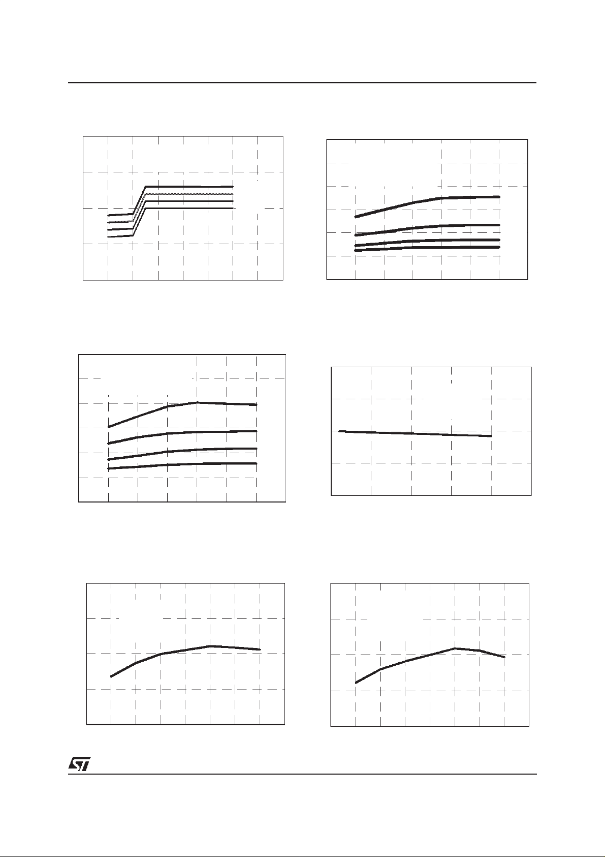
Figure 1. L5991 - Quiescentcurrent vs. input
voltage.
(X = 7.6V and Y= 8.4V for L5991A)
Iq [m A]
30
20
8
6
4
0.2
0.15
0.1
0.05
0
0 4 8 12162024
4/23
V 14 = 0, P in2 = ope n
Tj = 25°C
X
Y
Vcc [V]
28
Figure2. L5991 - Quiescentcurrent vs.input
voltage (after disable).
(X = 7.6V and Y= 8.4V for L5991A)
Iq [µ A]
350
300
250
200
150
100
50
0
0 4 8 12162024
X
Vcc [V]
V14 = Vref
Tj = 25 °C
Y
L5991 - L5991A
Figure 3. Quiescent currentvs. input voltage.
Iq [mA]
9.0
V14= 0, V5 = Vref
8.5
8.0
7.5
7.0
8 1012141618202224
Rt = 4.5K ohm ,Tj = 25° C
1Mhz
100Khz
Vcc [V]
500Khz
300Khz
Figure 5. Quiescent currentvs. input voltage
and switchingfrequency.
Iq[mA]
36
Co= 1nF,Tj = 25°C
30
24
DC= 100%
1MHz
Figure4. Quiescentcurrent vs. input voltage
and switchingfrequency.
Iq [m A]
36
30
24
18
12
6
0
Co = 1nF, Tj = 25°C
DC = 0 %
1M Hz
500KHz
300KHz
100KHz
8 10121416182022
Vcc [V]
Figure6. Reference voltage vs. load current.
Vref [V]
5.1
5.05
Vcc=15V
Tj= 25°C
18
12
6
0
8 10121416182022
Vcc[V]
500KHz
300KHz
100KHz
Figure 7. Vref vs. junctiontemperature.
Vref [V])
5.1
5.05
5
4.95
4.9
-50 -25 0 25 50 75 100 125 150
Vcc = 15V
Iref = 1mA
Tj (°C)
5
4.95
4.9
0 5 10 15 20 25
Iref [mA]
Figure8. Vref vs. junctiontemperature.
Vref [V]
5.1
Vcc = 15V
5.05
5
4.95
4.9
-50 -25 0 25 50 75 100 125 150
Iref= 20mA
Tj (°C)
5/23
L5991 - L5991A
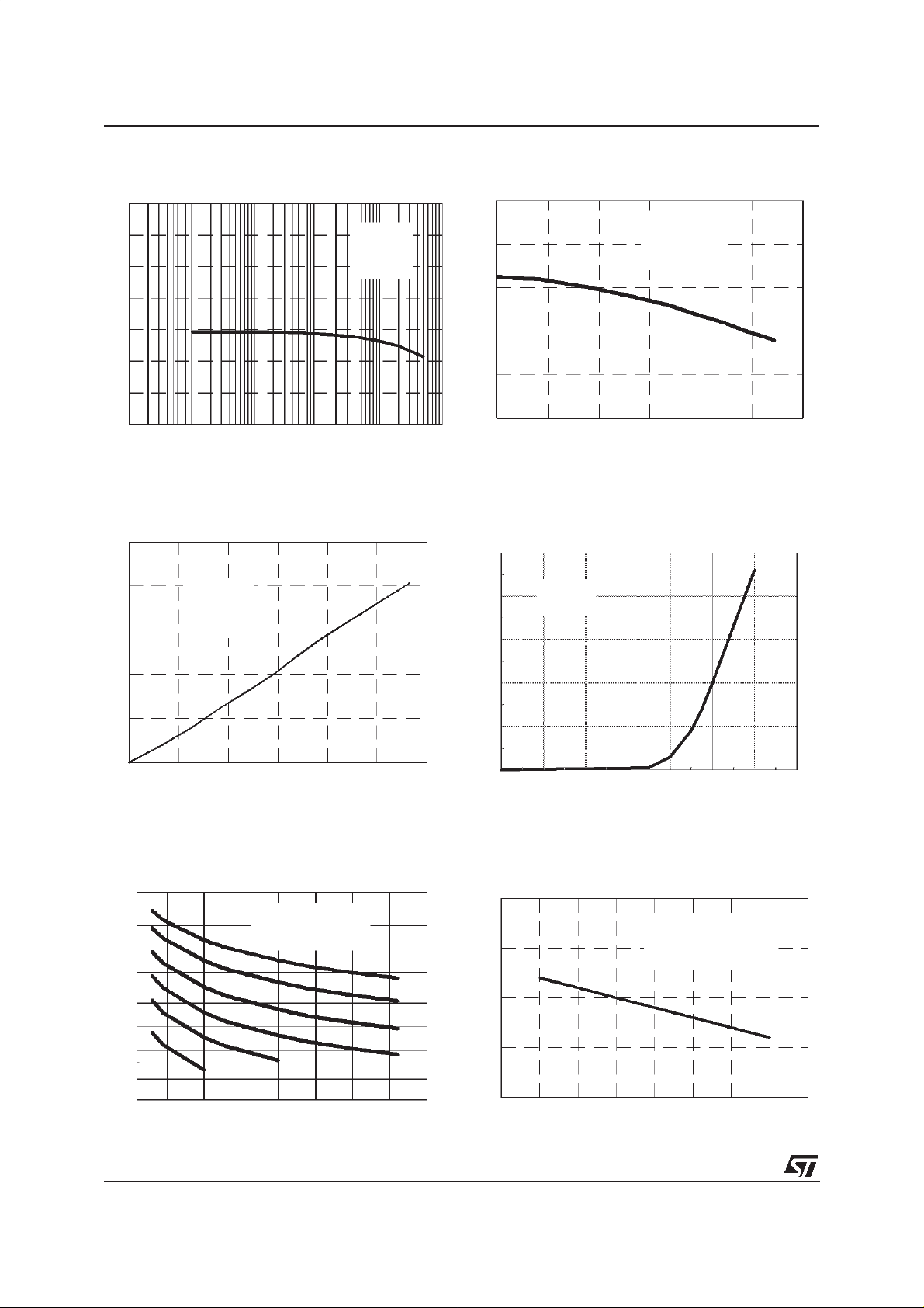
Figure 9. Vref SVRR vs. switchingfrequency.
SVRR (dB)
120
80
40
0
1 10 100 1000 10000
fsw (Hz)
Vcc=15V
Vp-p=1V
Figure 11. Outputsaturation.
Vsat = V [V]
2.5
2
1.5
10
Vcc = Vc = 15V
Tj= 25°C
Figure10. Outputsaturation.
Vsat = V [V]
16
14
12
10
8
6
0 0.2 0.4 0.6 0.8 1 1.2
10
Vcc = Vc = 15V
Tj = 2 5 °C
Isource [A]
Figure12. UVLO Saturation
Ipin10 [mA]
50
40
30
Vcc < Vccon
beforeturn-o n
1
0.5
0
0 0.2 0.4 0.6 0. 8 1 1.2
Isink [A ]
Figure13.Timingresistorvs.switchi n gfrequency.
fsw (KHz)
5000
2000
1000
500
200
100
50
20
10
5.6nF
10 20 30 40
Vcc = 15V, V15 =0V
Tj = 25°C
2.2nF
Rt (kohm)
100pF
220pF
470pF
1nF
20
10
0
0 200 400 600 800 1,000 1,200 1,400
Vpin10 [mV]
Figure14. Switching frequency vs. tempera-
ture.
fsw (KHz)
320
Rt= 4.5Kohm, Ct = 1nF
310
300
290
280
-50 -25 0 25 50 75 100 125 150
Vcc = 15V,V15=Vref
Tj (°C)
6/23

L5991 - L5991A
Figure 15.Switchingfrequencyvs. temperature.
fsw (KHz)
320
Rt= 4.5Kohm, Ct = 1nF
310
Vcc = 15V,V15= 0
300
290
280
-50 -25 0 25 50 75 100 125 150
Tj (°C)
Figure 17. Maximum Duty Cycle vs Vpin3.
DC Control Voltage Vpin3 [V]
3.5
V15 = Vref
3
V15 = 0V
Figure16. Dead time vs Ct.
Deadtime[ns]
1,500
Rt =4.5Kohm
V15= 0V
1,200
900
V15= Vref
600
300
246810
TimingcapacitorCt [nF]
Figure18.Delaytooutputvsjunctiontemperature.
Delay to output (ns)
42
40
2.5
2
Rt = 4.5Kohm,
1.5
Ct = 1nF
1
0 102030405060708090100
Duty Cycle [%]
Figure 19. E/A frequency response.
G [dB]
150
100
50
Phase
140
120
100
80
60
38
36
34
32
30
28
-50 -25 0 25 50 75 100 125 150
Tj (°C)
PIN10 = OPEN
1V pulse
on PIN13
0
40
20
0.01 0.1 1 10 100 1000 10000 100000
f(KHz)
7/23

L5991 - L5991A
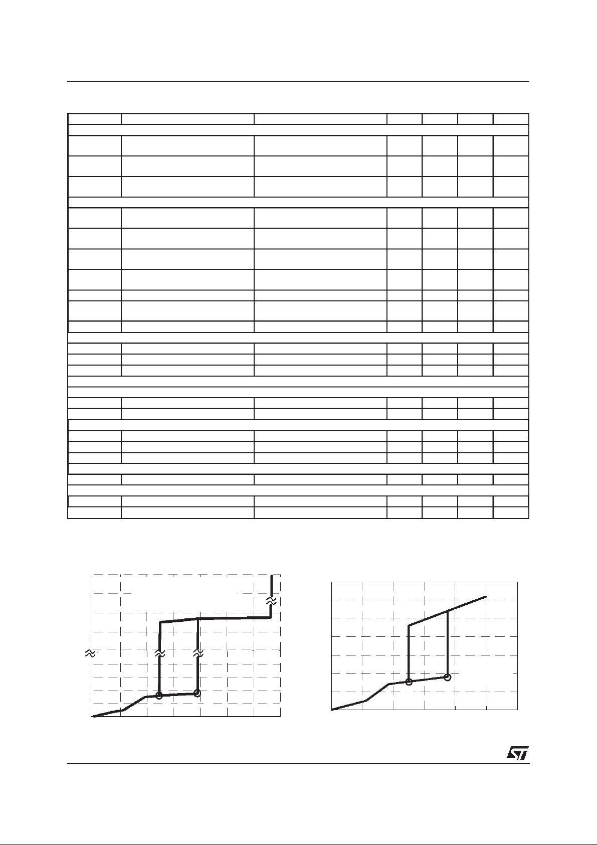
STANDBYFUNCTION
The standby function, optimized for flyback topology, automatically detects a light load condition
for the converter and decreases the oscillator frequency on that occurrence. The normaloscillation
frequency is automaticallyresumed when the output load builds up and exceeds a defined threshold.
This function allows to minimize power losses related to switching frequency, which represent the
majority of losses in a lightly loaded flyback, without givingup the advantagesof a higher switching
frequency at heavy load.
This is accomplished by monitoring the output of
the Error Amplifier (V
) that depends linearly
COMP
on thepeak primary current,except for an offset.
If the the peak primary currentdecreases (as a re-
sult of a decrease of the power demandedby the
load) and V
(V
), the oscillator frequency will be set to a
T1
lower value (f
increases and V
(V
) the oscillator frequency is set to the normal
T2
value (f
). An appropriate hysteresis (VT2-VT1)
osc
falls below a fixed threshold
COMP
). When the peak primary current
SB
exceedsa secondthreshold
COMP
prevents undesired frequency change when
power is such that V
moves close to the
COMP
threshold.This operationis shown in fig. 20.
Both the normal and the standby frequency are
externally programmable. V
and VT2are inter-
T1
nally fixed but it is possible to adjust the thresholds in terms of input power level.
Figure20. Standby dynamic operation.
Pin
f
osc
Normal operation
P
NO
P
SB
V
T
1234
1
Stand-by
fSB
V
T
2
VCOMP
maticallythe master.
During the ramp-up of the oscillator the pin is
pulled low by a 600µA internal sink current generator. During the falling edge, that is when the
pulse is released, the 600µA pull-down is disconnected. The pin becomes a generator whose
source capability is typically 7mA (with a voltage
still higher than3.5V).
In fig. 21, some practical examples of synchronizing the L5991 are given.
Since the device automatically diminishes its operating frequency under light load conditions, it is
reasonable to suppose that synchronization will
referto normal operationand not to standby.
APPLICATIONINFORMATION
Detailed Pin FunctionDescription
Pin 1. SYNC (In/Out Synchronization).This func-
tion allows the IC’s oscillator either to synchronize
other controllers (master) or to be synchronizedto
an externalfrequency(slave).
As a master, the pin delivers positive pulses during the falling edge of the oscillator (see pin 2). In
slave operationthe circuit is edgetriggered. Refer
to fig. 22 to see how it works. When several IC
work in parallel no master-slave designation is
needed because the fastest one becomes auto-
Figure 21. Synchronizingthe L5991.
R
B
ST-BY
1
16
L5991 L5991
VREF
4
2
R
A
C
T
(a) (b) (c)
SYNCSYNC
R
OSC
L4981A
(MASTER)
16
1817
C
OSC
1
2
RCTRCT
(SLAVE)
1
RCT
ST-BY
L5991
Pin 2.
RCT (Oscillator).Two resistors (R
and one capacitor (C
), connected as shown in
T
fig. 22, allow to set separately the operating frequency of the oscillator in normal operation (f
and in standbymode (f
C
is charged from Vrefthrough RAand RBin nor-
T
SB
).
mal operation (STANDBY = HIGH), through R
only in standby ( STANDBY = LOW). See pin 16
descriptionto see howtheSTANDBY signalisgenerated.
When the voltage on C
reaches 3V, the capaci-
T
tor is quickly internally discharged.As the voltage
has droppedto 1V it startsbeing charged again.
R
A
16
4
2
R
B
VREFSYNC
R
A
C
T
RCT
R
B
C
T
D97IN728A
4
L5991
(MASTER)
16
ST-BY
VREF
12
SYNC
SYNC
16
R
OSC
A
L4981A
(SLAVE)
17 18
and RB)
osc
C
OSC
)
A
8/23

Figure 22. Oscillatorand synchronizationinternalschematic.
V
4
REF
L5991 - L5991A
SYNC
1
R1
CLAMP
R
A
RCT
2
R
B
C
T
16ST-BY
D1
50Ω
STANDBY
R2R3
The oscillation frequency can be established with
the aid of the diagrams of fig.13, where R
intended as the parallel of R
operation and R
=RAin standby,or considering
T
and RBin normal
A
will be
T
the followingapproximate relationships:
f
osc
≅
⋅ (
C
0.693
T
⋅ (
1
)+
// R
R
A
B
K
(1),
T
which gives the normal operatingfrequency,and:
≅
f
SB
C
T
1
⋅ (0.693 ⋅ RA+ K
(2),
)
T
which gives the standby frequency,that is the one
the converter will operateat when lightly loaded.
In the above expressions,RA // RB means:
RA⋅ R
R
+ R
A
/OPEN
B
,
B
(3)
,
while K
R
is defined as:
T
90 V15= VREF
=
K
T
160
A
//R
V
B
= GND
15
=
D
Q
R
600µA
+
-
D97IN729A
CLK
fromfig.13 or resultingfrom (1) and (2).
To prevent the oscillator frequency from switching
back and forth from f
to fSB, the ratio f
osc
mustnot exceed5.5.
If during normal operation the IC is to be synchro-
nized to an external oscillator, R
should be selected for a f
lowerthan the master
osc
,RBand C
A
frequency in any condition (typically, 10-20% ),
dependingalso on the toleranceof the parts.
Pin 3.
DC (Duty Cycle Control). By biasing this
pin with a voltage between1 and 3 V it is possible
to set the maximum duty cycle between 0 and the
upper extremeD
If D
is the desired maximum duty cycle, the
max
(seepin 15).
x
voltageV3 to be applied to pin 3 is:
=5-2
(2-Dmax)
(5)
V
3
is determined by internal comparison be-
D
max
tween V3 and the oscillator ramp (see fig. 23),
thus in case the device is synchronized to an external frequency f
(and therefore the oscillator
ext
amplitudeis reduced),(5) changesinto:
osc/fSB
T
and is related to the duration of the falling-edge of
the sawtooth:
10
−9
+
⋅ C
K
T
(4)
.
T
≈ 30⋅
T
d
is also the duration of the sync pulses deliv-
T
d
ered at pin 1 and definesthe upperextreme of the
duty cycle range, D
(see pin 15 for DXdefinition
x
and calculation) since the output is held low during thefalling edge.
In case V15 is connected to VREF, however, the
switchingfrequencywill be a halfthe values taken
V
= 5 − 4 ⋅ exp
3
−
R
T⋅CT
D
max
⋅f
ext
(6)
A voltage below 1V will inhibit the driver output
stage.This could be used for a not-latcheddevice
disable, for example in case of overvoltage protection(see applicationideas).
If no limitation on the maximum duty cycle is required (i.e. D
MAX=DX
), the pin has to be left floating. An internal pull-up (see fig. 23) holds the voltage above 3V. Should the pin pick up noise (e.g.
9/23

L5991 - L5991A
during ESD tests), it can be connected to VREF
through a 4.7kΩ resistor.
Figure 23. Duty cycle control.
4
V
REF
Pin 4.
R1
DC
R2
R
A
ST-BY
R
B
RCT
C
T
VREF (Reference Voltage). The device is
3µA
3
16
+
2
-
D97IN727A
23K
28K
TO PWM LOGIC
provided with an accurate voltage reference
(5V±1.5%)able to deliver some mA to an external
circuit.
A small film capacitor (0.1µF typ.), connected
between this pin and SGND, is recommended to
ensure the stability of the generator and to prevent
noisefromaffectingthereference.
Beforedevice turn-on,thispin has a sinkcurrentcapabilityof0.5mA.
Pin 5. VFB (Error Amplifier Inverting Input). The
feedback signal is applied to this pin and is compared to the E/A internal reference (2.5V). The
E/A output generates the control voltage which
fixes the duty cycle.
The E/A features high gain-bandwidth product,
which allows to broaden the bandwidth of the
overall control loop, high slew-rate and current capability, which improves its large signal behavior.
Usually the compensation network, which stabilizes the overall control loop, is connected between this pin and COMP(pin 6).
Pin 6.
COMP (Error Amplifier Output). Usually,
this pin is used for frequency compensation and
the relevant network is connected between this
pin and VFB (pin 5). Compensation networks towards ground are not possible since the L5991
E/A is a voltage mode amplifier (low output impedance). See application ideas for some example ofcompensationtechniques.
It is worth mentioning that the calculation of the
part values of the compensation network must
take the standby frequency operation into account. In particular,this means that the open-loop
crossover frequency must not exceed f
/5.
f
SB
SB
/4 ÷
The voltage on pin 6 is monitored in order to re-
10/23
duce the oscillator frequency when the converter
is lightly loaded (standby).
Pin 7. SS (Soft-Start). At device start-up, a capacitor (Css) connected between this pin and
SGND (pin 12) is charged by an internal current
generator, ISSC, up to about 7V. During this
ramp, the E/A output is clamped by the voltage
across Css itself and allowed to rise linearly, starting from zero, up to the steady-state value imposed by the control loop. The maximum time interval during which the E/A is clamped, referredto
as soft-starttime,is approximately:
3⋅R
≅
T
ss
whereR
13) and I
through R
is the current sense resistor (see pin
sense
is the switch peak current (flowing
Qpk
sense
load. Usually, C
), which depends on the output
SS
⋅
I
sense
I
SSC
Qpk
⋅ C
ss
(7)
is selected for a TSSin the or-
der of milliseconds.
As mentioned before, the soft-start intervenes
also in case of severe overload or short circuit on
the output. Referring to fig. 24, pulse-by-pulse
current limitation is somehow effective as long as
Figure24. Regulation characteristicand re-
latedquantities.
V
OUT
T
ON
D97IN495
D.C.M. C.C.M.
I
SHORTIOUT(max)
A
B
D
I
Qpk
1-2 ·I
Qpk
I
Qpk(max)
C
T
ON(min)
I
OUT
the ON-time of the power switch can be reduced
(from A to B). After the minimum ON-time is
reached (from B onwards) the current is out of
control.
To prevent this risk, a comparator trips an overcurrent handling procedure, named ’hiccup’ mode
operation,when a voltage above 1.2V (point C) is
detected on current sense input (ISEN, pin 13).
Basically,the IC is turned off and then soft-started
as long as the fault condition is detected.As a result, the operating point is moved abruptly to D,
creating a foldback effect. Fig. 25 illustrates the
operation.
The oscillation frequency appearing on the softstart capacitorin case of permanentfault, referred
to as ’hiccup” period, is approximatelygiven by:
T
hic
≅ 4.5 ⋅
I
SSC
1
1
+
I
SSD
⋅ C
(8)
ss

L5991 - L5991A
Since the system tries restarting each hiccup cycle, there is not any latchoff risk.
”Hiccup” keeps the system in control in case of
short circuits but does not eliminate power components overstress during pulse-by-pulse limitation (from A to C). Other external protection circuits are needed if a better control of overloads is
required.
Pin 8.
VCC (Controller Supply). This pin supplies
the signalpart of the IC. The device is enabled as
VCC voltage exceeds the start threshold and
works as long as the voltage is above the UVLO
threshold. Otherwise the device is shut down and
the current consumption is extremely low
(<150µA). This is particularly useful for reducing
the consumptionof the start-upcircuit (in the simplest case, just one resistor), which is one of the
most significant contributions to power losses in
standby.
An internal Zener limits the voltage on VCC to
25V. The IC current consumption increases considerablyif this limit is exceeded.
A small film capacitor between this pin and SGND
(pin 12), placed as close as possible to the IC, is
recommendedto filterhigh frequencynoise.
Pin 9. VC (Supply of the Power Stage). It supplies
the driver of the external switch and therefore absorbs a pulsedcurrent. Thus it is recommendedto
place a buffer capacitor (towards PGND, pin 11,
as close as possible to the IC) able to sustain
these current pulses and in order to avoid them
inducingdisturbances.
This pin can be connected to the buffer capacitor
directly or through a resistor, as shown in fig. 26,
to control separately the turn-on and turn-off
speed of the external switch, typically a Power-
Figure 25. Hiccup mode operation.
MOS.At turn-on the gate resistance is R
turn-offis R
g
only.
g+Rg’
,at
Figure26. Turn-on and turn-offspeeds adjust-
ment.
Rg’
DRIVE
CONTROL
L5991
D97IN726
Pin 10.
V
CC
8
13V
&
PGND
V
C
9
10
OUT
Rg
11
OUT (Driver Output). This pin is the out-
Rg(ON)=Rg+Rg’
Rg(OFF)=Rg
put of the driver stage of the external power
switch. Usually, this will be a PowerMOS, although the driver is powerful enough to drive
BJT’s(1.6Asource,2A sink,peak).
The driver is made up of a totempole with a highside NPN Darlington and a low-sideVDMOS, thus
there is no need of an external diode clamp to
prevent voltage from going below ground. An internal clamp limits the voltage delivered to the
gate at 13V. Thus it is possible to supply the
driver (Pin 9) with higher voltageswithout any risk
of damage for thegate oxide of the externalMOS.
The clamp does not cause any additional increase of power dissipation inside the chip since
the current peak of the gate charge occurs when
the gate voltage is few volts and the clamp is not
active. Besides, no current flows when the gate
voltageis 13V,steady state.
Under UVLO conditionsan internal circuit (shown
I
OUT
I
SEN
FAULT
SS
5V
0.5V
SHORT
7V
T
hic
D98IN986
time
11/23

L5991 - L5991A
in fig.27) holds the pin low in order to ensure that
the external MOS cannot be turned on accidentally. The peculiarity of this circuit is its ability to
mantain the same sink capability (typically, 20mA
@ 1V) from V
= 0V up to the start-upthreshold.
CC
When the threshold is exceeded and the L5991
starts operating,V
is pulled high (refer to fig.
REFOK
27) and thecircuit is disabled.
It is then possible to omit the ”bleeder” resistor
(connected between the gate and the source of
the MOS) ordinarily used to prevent undesired
switching-on of the external MOS because of
some leakage current.
Figure 27. Pull-Downof the output in UVLO.
OUT
10
V
REFOK
12
SGND
D97IN538
Pin 11.
PGND (Power Ground). The current loop
during the discharge of the gate of the external
MOS is closed through this pin. This loop should
be as short as possible to reduce EMI and run
separatelyfrom signal currents return.
Pin 12
. SGND(Signal Ground). This groundreferences the control circuitry of the IC, so all the
ground connections of the external parts related
to control functions must lead to this pin. In laying
out the PCB, care must be taken in preventing
switched high currents from flowing through the
SGND path.
Pin 13.
ISEN (Current Sense). This pin is to be
connected to the ”hot” lead of the current sense
resistor R
(being the other one grounded), to
sense
get a voltage ramp which is an image of the current of the switch (I
). When this voltage is equal
Q
to:
V
13pk
= I
Qpk
⋅ R
sense
V
=
COMP
3
− 1.4
(9)
the conductionof the switchis terminated.
To increase the noise immunity, a ”Leading Edge
Blanking” of about 100ns is internally realized as
shown in fig. 28. Because of that, the smoothing
RC filter between this pin and R
sense
could be re-
movedor, at least, considerablyreduced.
Pin 14.
DIS (Device Disable). When the voltage
on pin 14 rises above 2.5V the IC is shut down
and it is necessaryto pull VCC(IC supply voltage,
pin 8) below the UVLO threshold to allow the device to restart.
The pin can be driven by an external logic signal
in case of power management, as shown in fig.
29. It is also possible to realize an overvoltage
protection, as shown in the section ” Application
Ideas”.Ifused, bypass this pin to ground with a filter capacitor to avoid spurious activation due to
noise spikes. If not, it must be connected to
SGND.
Pin 15. DC-LIM (Maximum Duty Cycle Limit). The
upper extreme, Dx, of the duty cycle range depends on the voltage applied to this pin. Approximately,
R
T
D
x
≅
RT+ 230
(
10)
if DC-LIM is grounded or left floating. Instead,
Figure 28. Internal LEB.
13
ISEN
12/23
I
1.2V
2V
3V
0
CLK
FROM E/A
+
OVERCURRENT
COMPARATOR
+
-
COMPARATOR
+
-
PWM
D97IN503
PWM
TO
LOGIC
TO FAULT
LOGIC

L5991 - L5991A
Figure 29. Disable (Latched).
DISABLE
SIGNAL
DIS
14
+
-
C
2.5V
D
R
UVLO
Q
DISABLE
D97IN502
connecting DC-LIM to VREF (half duty cycle option), Dx will be set approximatelyat:
R
D
≅
x
T
2 ⋅ RT+ 260
(11)
Figure 30. Half duty cycle option.
t
d
V15=GND
V5=V13=GND
and the output switching frequency will be halved
with respect to the oscillator one because an internal T flip-flop (see block diagram) is activated.
Fig. 30 shows the operation.
The half duty cycle option speeds up the discharge of the timing capacitor C
(in order to get
T
duty cycles as close to 50% as possible) so the
oscillatorfrequency- with thesame timing componentswill be slightlyhigher.
Pin 16
. S-BY(Standby Function).The resistorR
along with R
oscillatorin normal operation(f
, sets the operating frequencyof the
A
osc
). In fact, as long
B
as the STANDBY signal is high, the pin is internally connected to the referencevoltage VREF by
a N-channel FET (see fig. 31), so the timing capacitor C
is charged through RAand RB. When
T
the STANDBY signal goeslow the N-channelFET
is turned off and the pin becomes floating. R
V2
DX=
t
c
tc+t
d
is
B
,
t
c
t
d
V15=VREF
V5=V13=GND
t
c
D97IN498
Figure 31. Standbyfunction internalschematicand operation.
COMP
6
5
FB VREF
-
+
2.5
2.5/4
ISEN
13
2R
R
+
LEVEL SHIFT
STANDBY BLOCK
+
-
10V
R
STANDBY
DRIVER OUT
4
ST-BY
16
2
RCT
R
B
V10
V2
V10
R
C
STANDBY
HIGH
LOW
A
T
DX=
2·tc+t
D97IN752B
t
c
VT1
2.5V
d
V
V
T2
4V
COMP
13/23

L5991 - L5991A
now disconnected and CTis charged through R
only. In this way the oscillator frequency (fSB) will
be lower. Refer to pin 2 descriptionto see how to
calculatethe timingcomponents.
Typical values for V
and VT2are 2.5 V and 4V
T1
respectively. This 1.5V hysteresis is enough to
prevent undesired frequency change up to a 5.5
to1 f
osc/fSB
The value of V
ratio.
is such that in a discontinuous
T1
flyback the standby frequency is activated when
the input power is about 13% of the maximum. If
necessary, it is possible to decrease the power
threshold below 13% by adding a DC offset (V
on the current sense pin (13, ISEN). This will also
allow a frequencychange greater than 5.5 to 1.
The following equations,useful for design,apply:
P
inSB
P
inNO
where P
0.367− V
1
=
⋅ LP⋅ƒ
2
1
=
⋅ LP⋅ƒSB⋅
2
ƒ
osc
<
ƒ
SB
is the input power below which the
inSB
⋅
osc
0.867− V
0.867 − V
0.367 − V
R
R
o
o
sense
sense
2
o
o
(14),
2
(12),
2
(13),
L5991 recognizes a light load and switches the
oscillator frequency from ƒ
to fSB,P
osc
inNO
is the
input power above which the L5991 switches
back from
ƒ
SB
to
ƒ
and Lpthe primary induc-
osc
tance of the flyback transformer.
Connect to Vref or leave open this pin when
stand-by functionis not used.
A
Layouthints
Generallyspeaking a proper circuitboard layout is
vital for correct operation but is not an easy task.
Carefulcomponent placing, correct traces routing,
appropriate traces widths and, in case of high
voltages, compliance with isolation distances are
the major issues. The L5991 eases this task by
putting two pins at disposal for separate current
returns of bias (SGND) and switch drive currents
(PGND) The matter is complex and only few importantpointswill be here reminded.
1) All current returns (signal ground, power
)
o
ground, shielding, etc.) should be routed separately and should be connected only at a single
ground point.
2) Noise coupling can be reduced by minimizing
the area circumscribed by current loops. This
applies particularly to loops where high pulsed
currentsflow.
3) For high current paths, the traces should be
doubled on the other side of the PCB whenever
possible: this will reduce both the resistance
and the inductanceof the wiring.
4) Magnetic field radiation (and stray inductance)
can be reduced by keeping all traces carrying
switchedcurrentsas shortas possible.
5) In general, traces carrying signal currents
should run far from traces carrying pulsed currents or with quickly swinging voltages. From
this viewpoint, particular care should be taken
of the high impedance points (current sense input, feedback input, ...). It could be a good idea
to route signal traces on one PCB side and
power traceson theother side.
6) Provide adequate filtering of some crucial
points of the circuit,such as voltage references,
IC’s supplypins, etc.
14/23

L5991 - L5991A
APPLICATIONIDEAS
Here follows a seriesof ideas/suggestionsaimedat
either improving performance or solving common
applicationproblems of L5991 based supplies.
Figure 32. Typicalapplicationcircuit for computer monitors (90W).
65W
180V
D52 BYT13-800
18
80V
10W
C62
C52
100µF
C54
D53 BYT11-600
16
17
GND
100µF 100V
250V
220µF 100V
6.3V
C55
D54 BYW100-100
151314
5W
16V
1000µF
5W
+15V
C56
470µF 25V
D55 BYW100-100
-15V
C57
470µF 25V
111210
5W
47
R52
D56 BYW100-100
C58
R53
47µF 25V
4.7K
C59
100K
VR51
D97IN730A
R56
4.3K
0.01µF
R55
300K
C61
0.056µF
R58
4.7K
C11 4700pF 4KV C12
R19 4.7M R20 4.7M
BD01
LF01
1
R01 3.3
C02
C01
0.1µF
0.1µF
C10
R18
R16
C03 220µF
10nF
100V
3W
47K
750K
400V
D05
1N4937
R17
D06
387
D04 1N4148
750K
R04 47K
R03 47K
1N4148
R07 47
C11 2.2nF
R12 330K
R06 27
R13 47K
1K
R54
Q01
STP6
NA60FI
R10
R08 22
C04 47µF
8
10
91416
C05
R11 1K
100pF
13
12
L5991
2
4
R5
12K
C06
C07 1µF
R9
24K
6800pF
16
0.22
4N35
R21 100
C08
3.3nF
6
11
5
7
C09 8.2nF
Q51
TL431
270
220
110
88
VAC(V)
4.40
3.90
2
3.10
2.95
Pin(W)
Pout(W)
F01 AC 250V T3.15A
88 to 270
VAC
15/23

L5991 - L5991A
Figure 33. Typicalapplicationcircuit for inkjet printers (40W).
4700pF 4KV 4700pF 4KV
28V / 0.7A
µF
35V
2 x 330
BYW100-200
N2
4.7M
4.7M
BZW06-154
12V / 1.5A
µF
2 x 470
BYW98-100
N3
N1
1N4937
10K
GND
16V
5V / 0.5A
µF
470
BYW100-50
N4
Naux
BAT46
16V
µF/25V
33
STP4NA60
22
0.47
1/2 W
470pF
1K
220
470
4N35
470pF
5.1K 270K
3.9K
µF
0.022
2.7K
TL431
D97IN618
16/23
F01 AC 250V T1A
BD01
LF01
2.2
C02
C01
85 TO
µF
0.1
0.1µF
265 Vac
µF
100
400V
1.1M
STK2N50
1.1M
BC337
22V
33K4.7K
47K
22
5.6K
100nF
8
10
91415
131K12
L5991
2
3
4
5.6K
22K
16
3.3nF
1
5.6K
6
11
5
265
1.57
220
7
330nF
1.14
110
0.93
85
0.90
Pin(W)
VAC(V)
0.55
Pout(W)

Figure 34. Standbythresholds adjustment.
L5991 - L5991A
SGND
L5991
12
10
413
VREF ISEN
R
A
D97IN751A
R
OPTIONAL
R
SENSE
Figure 35. Isolated MOSFETDrive & Current TransformerSensing in 2-switch Topologies.
V
IN
PGND
L5991
1112
V
9
SGND
ISOLATION
C
OUT
10
ISEN
13
BOUNDARY
D97IN761
Figure 36. Low consumptionstart-up.
2.2MΩ 33KΩ
20V
47KΩ
D97IN762B
Figure 37. Bipolartransistor driver.
L5991
V
IN
STD1NB50-1
V
4
CC
8
L5991
V
REF
T
SELF-SUPPLY
WINDING
12 11
V
IN
V
8
V
CC
C
9
11
PGND
OUT
10
ISEN
13
D97IN763
17/23

L5991 - L5991A
Figure 38. TypicalE/A compensationnetworks.
From V
O
R
i
R
C
d
f
COMP
Error Amp compensation circuit for stabilizing any current-mode topology
for boost and flyback converters operating with continuous inductor current.
From V
O
R
P
R
i
C
P
C
R
d
f
COMP
Error Amp compensation circuit for stabilizing current-mode boost and
topologies operating with continuous inductor current.
Figure 39. Feedback withoptocoupler.
VFB
R
VFB
R
2.5V
+
1.3mA
+
5
EA
f
6
2R
R
12
SGND
except
EA
+
1.3mA
2R
R
12
SGND
D97IN507
2.5V
+
5
-
f
6
flyback
COMP
6
L5991
5
VFB
Figure 40. Slope compensationtechniques.
ST-BY 16
16
V
REF
4
R
B
R
I
R
SLOPE
SENSE
R
A
RCT
C
T
ISEN
OPTIONAL
2
13
L5991
12
SGND
I
R
SLOPE
R
SENSE
R
B
ST-BY
V
REF
R
A
RCT
C
T
ISEN
OPTIONAL
TL431
D97IN759
4
2
L5991
13
12
SGND
V
OUT
SGND
D97IN760A
L5991
12
10
13
OPTIONAL
OUT
ISEN
R
C
SLOPE
R
SLOPE
R
SENSE
18/23

Figure 41. Protectionagainst overvoltage/feedbackdisconnection(latched)
L5991 - L5991A
R
START
V
CC
14
L5991
12 11
SGND
8
PGND
D97IN754
DIS
Figure 42 Protectionagainst overvoltage/feed-
back disconnection(not latched)
R
START
V
VREF
DC
CC
4
8
L5991
3
12
11
D97IN755A
R
START
V
V
Z
DIS
2.2K
CC
14
L5991
12 11
SGND
8
PGND
D98IN905
Figure43. Device shutdown on overcurrent
2.5
≅
R
R
2
R
SENSE
I
SENSE
1-
I
pk
PGND
L5991
SGND
14
13
1211
VREF
4
DIS
ISEN
OPTIONAL
R
1
D97IN756A
I
pk max
R
2
•
R
1
Figure 44. Constantpower in pulse-by-pulsecurrent limitation(flyback discontinuous)
V
IN
80 ÷
PGND
400V
L5991
DC
OUT
SGND
10
R
FF
ISEN
13
1211
L
p
R·L
p
RFF= 6·10
R
R
SENSE
6
R
D97IN757
SENSE
Figure 45. Voltage mode operation.
DC
3
10K
COMP
L5991
6
12 13
SGND ISEN
D97IN758A
19/23
 Loading...