

2A SWITCH STEP DOWN SWITCHING REGULATOR
■ 2A INTERNAL SWITCH
■ OPERATING INPUT VOLTAGE FROM 4.4V
TO 36V
■ OUTPUT VOLTAGE ADJUSTABLE FROM
1.235V TO 35V
■ LOW DROPOUT OPERATION: 100% DUTY
CYCLE
■ 250KHz INTERNALLY FIXED FREQUENCY
■ VOLTAGE FEEDFO RWA R D
■ ZERO LOAD CURRENT OPERATION
■ INTERNAL CURRENT LIMITING
■ PROTECTION AGAINST FEEDBACK
DISCONNECTION
■ THERMAL SHUTDOWN
APPLICATIONS:
■ CONSUMER: STB, DVD, TV, VCR,CAR
RADIO, LCD MONITORS
■ NETWORKING: XDSL, MODEMS,DC-DC
MODULES
■ COMPUTER: PRINTERS, AUDIO/GRAPHIC
CARDS, OPTICAL STORAGE, HARD DISK
DRIVE
■ INDUSTRIAL: CHARGERS, CAR BATTERY
DC-DC CONVERTERS
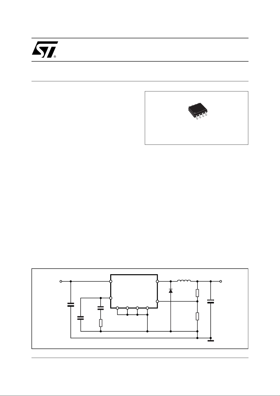
L5972D
SO8 (4+2+2)
ORDERING NUMBERS: L5972D (SO8)
L5972D013TR (Tape & Reel)
DESCRIPTION
The L5972D is a step down monolithic power switching regulator with a minimum switch current limit of
2A so it is able to deliver more than 1.5A DC current
to the load depending on the application conditions.
The output voltage can be set from 1.235V to 35V.
The device uses an internal P-Channel D-MOS tran-
sistor (with a typical Rdson of 250m
element to minimize the s i ze of t he ext ernal c omponents.
An internal oscillator fixes the switching frequency at
250KHz.
Having a minimum input voltage of 4.4V only, it is
particularly suitable for 5V bus, availabl e in all computer related applications.
Pulse by pulse current limit with the internal frequency modulation offers an effective constant current
short circuit protection.
Ω
) as swi tch ing
TEST APPLICATION CIRCUIT
VIN = 4.4V to 35V
C1
10µF
35V
CERAMIC
May 2003
C4
22nF
C3
220pF
VCC OUT
COMP
R3
4.7K
8
4
6
L5972D
2
3
1
5
7
GND
D03IN1436
FB
L1 33µH
D1
STPS2L40U
R1
5.6K
R2
3.3K
VOUT=3.3V
C2
100µF
10V
1/10
L5972D
PIN CONNECTION
OUT
GND
GND
COMP
1
2
3
4
8
7
6
5
D02IN1367
VCC
GND
GND
FB
PIN DESCRIPT ION
N° Pin Function
1 OUT Regulator Output.
2,3,6,7 GND Ground.
4 COMP E/A output for frequency compensation.
5 FB Feedback input. Connecting directly to this pin results in an output voltage of 1.23V. An external
resistive divider is required for higher output voltages.
8 VCC Unregulated DC input voltage.
THERMAL DATA
Symbol Parameter Value Unit
R
th (j-amb)
(*) Package mounted on board (4cm2 ground-plane)
Thermal Resistance Junction to ambient Max. 65 (*) °C/W
ABSOLUTE MAXIMUM RATINGS
Symbol Parameter Value Unit
Input Voltage 40 V
8
Out pin DC voltage
1
Out pin peak voltage at ∆t = 0.1µs
Maximum output current int. limit.
Analog pins 4 V
5
Power dissipation at Tamb ≤ 70°C 1.2 W
Operating junction temperature range -40 to 150 °C
j
Storage temperature range -55 to 150 °C
-1 to 40
-5 to 40
2/10
V
V
I
1
V4, V
P
tot
T
T
stg
V
V
L5972D
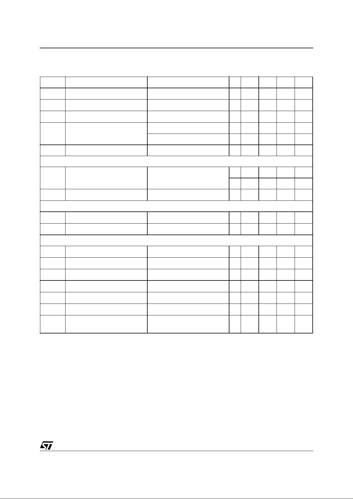
ELECTRICAL CHARACTERISTICS
(Tj = 25°C, VCC = 12V, unless otherwise specified.)
(*) Specification Referred to Tj from -40 to 125°C.
Symbol Parameter Test Condition Min. Typ. Max. Unit
V
DYNAMIC CHARACTERISTICS (see test circuit ).
DC CHARACTERISTICS
I
Operating input voltage range Vo = 1.235V; Io = 1.5A * 4.4 36 V
CC
V
Dropout voltage VCC = 4.4V; Io = 1.5A * 0.375 0.75 V
d
I
Maximum limiting current VCC = 4.4V to 36V * 2 2.5 3 A
l
Switching frequency * 212 250 280 KHz
f
s
225 250 275 KHz
Duty cycle 0 100 %
Voltage feedback 4.4V < VCC < 36V,
V
5
20mA < IO < 1.5A
h Efficiency V
Total operating quiescent current * 3 5 mA
qop
I
Quiescent current Duty Cycle = 0; VFB = 1.5V 2.5 mA
q
= 5V, VCC = 12V 90 %
O
1.220 1.235 1.25 V
* 1.198 1.235 1.272 V
ERROR AMPLIFIER
V
V
I
o source
I
o sink
High level output voltage VFB = 1V 3.5 V
OH
Low level output voltage VFB = 1.5V 0.4 V
OL
Source output current V
Sink output current V
I
Source bias current 2.5 4 µA
b
DC open loop gain RL = ∞ 50 65 dB
gm Transconductance I
= 1.9V; VFB = 1V 200 300 µA
COMP
= 1.9V; VFB = 1.5V 1 1.5 mA
COMP
= -0.1mA to 0.1mA
comp
V
= 1.9V
COMP
2.3 mS
3/10

L5972D
(A)
Figure 1. Out put V ol t age v s. Junction
Temperature
Vo (V)
3.312
3.308
Vcc = 12V
Vo = 3.3V
3.304
3.3
Tj = 25°C
3.296
3.292
3.288
3.284
Tj = 125°C
3.28
3.276
00.511.5
Io
Figure 2. Line R egulation
Vo (V)
3.312
3.308
3.304
3.296
3.292
3.288
3.284
3.276
Vcc = 12V
Vo = 3.3V
3.3
3.28
010203040
Tj = 25°C
Tj = 125°C
Vcc (V)
Figure 3. Out put V ol t age v s. Junction
Temperature
Vo (V)
1.25
1.24
1.23
Figure 4. Quiescent Current vs. Junction
Iq (mA)
2
1.8
1.6
Vcc = 12V
1.4
1.2
-50
DC = 0%
050
Tj (°C)
100 150
Figure 5. Shutdown Curr ent vs. J un ct io n
Temperature
Ishd (µA)
70
60
50
40
30
-50
Vcc = 12V
0
50 100 150
Tj (°C)
Figure 6. Switching Frequency vs.Junction
Temperature
Iq (mA)
2
1.8
1.22
Vcc = 12V
1.21
Vcc=12V
1.2
-50 0 50 100 150
Tj (°C)
4/10
1.6
1.4
1.2
-50
Vcc = 12V
DC = 0%
050
Tj (°C)
100 150

L5972D
APPLICATION CIRCUIT
In figure 7 is shown the demo board application circuit for the device in SMD version, where the input supply
voltage, Vcc, can range from 4.4V to 25V due to the rated voltage of the input capacitor and the output voltage
is adjustable from 1.235V to V
Figure 7. Demo board Application Circuit
.
cc
VIN = 4.4V to 25V
C1
10µF
25V
CERAMIC
C4
22nF
C3
220pF
VCC OUT
COMP
R3
4.7K
8
4
6
L5972D
2
3
1
5
7
GND
D03IN1438
FB
L1 33µH
D1
STPS2L25U
Table 1. Component List
Reference Part Number Description Manufacturer
C1 10µF, 25V TOKIN
C2 POSCAP 10TPB100M 100µF, 10V Sanyo
C3 C1206C221J5GAC 220pF, 5%, 50V KEMET
R1
5.6K
R2
3.3K
VOUT=3.3V
C2
100µF
10V
C4 C1206C223K5RAC 22nF, 10%, 50V KEMET
R1 5.6K, 1%, 0.1W 0603 Neohm
R2 3.3K, 1%, 0.1W 0603 Neohm
R3 4.7K, 1%, 0.1W 0603 Neohm
D1 STPS2L25U 2A, 25V ST
L1 DO3316P-333 33µH, 2.1A COILCRAFT
5/10

L5972D
Figure 8. PC B lay o ut (c om po nent side)
Figure 9. PC B lay o ut (bot t om si de)
42mm
34mm
Figure 10. PC B layout (front si de)
Sideways two graphs show the Tj versus output current in different conditions of the input and output voltage.
6/10

L5972D
Figure 11. Junction Temperature vs. Output
Current
TJ(°C)
100.0
90.0
80.0
70.0
Vin=5V
Tamb.=25°C
Vo=2.5V
Vo=3.3V
Vo=1.8V
60.0
50.0
40.0
30.0
20.0
0.2 0.4 0.6 0.8 1 1.2 1.4 1.6 1.8 2
Io(A)
Figure 12. Junction Temperature vs. Output
Current
TJ(°C)
100.0
90.0
80.0
Vin=12V
Tamb= 25°C
Vo=5V
70.0
60.0
50.0
40.0
30.0
20.0
0.2 0.4 0.6 0.8 1 1.2 1.4 1.6 1.8 2
Io(A)
Vo=2.5V
Vo=3.3V
Figure 13. Efficiency vs. Output Current
95
93
91
89
87
85
83
81
79
77
Efficiency (%)
75
73
71
69
67
0.1 0.3 0.5 0.7 0.9 1.1 1.3 1.5 1.7
Vcc=5V
Vo=1.8V
Vo=1.8V
Vo=2.5V
Vo=2.5V
Vo=3.3V
Vo=3.3V
Io (A)
Figure 14. Efficiency vs. Output Current
96
94
92
90
88
86
84
82
80
Efficiency (%)
78
76
74
72
70
Vin=12V
Vin=12V
0.1 0.3 0.5 0.7 0.9 1.1 1.3 1.5 1.7
Vo=3.3V
Vo=3.3V
Vo=2.5V
Vo=2.5V
Vo=5V
Vo=5V
Io (A)
7/10

L5972D
APPLICATION IDEAS
Figure 15. Positive Buck-Boost regulator
VIN=5V
Vcc
8
C1
10uF
10V
Ceramic
C2
220pF
C3
22nF
R3
4.7k
COMP
L5972D
4
2
Figure 16. Buck-Boost regulator
VIN=5V
C1
10uF
10V
Ceramic
C2
10uF
25V
Ceramic
C3
220pF
Vcc
COMP
C4
22nF
R3
4.7k
6
GND
OUT
L1
33uH
D2
STPS2L25U
VOUT=12V/0.45A
1
D1
STPS2L25U
FB
5
3
7
M1
STN4NE03L
24k
2.7k
C4
100uF
16V
L1
OUT
8
L5972D
4
6
2
GND
1
FB
5
3
7
2.7k
24k
33uH
D1
STPS2L25U
C5
100uF
16V
VOUT=-12V/0.45A
Figure 17. Dua l ou t put v ol tage with auxili ary wi nding
8/10
VIN=12V
C1
10uF
25V
C2
220pF
C3
22nF
R3
4.7k
Vcc
COMP
8
L5972D
4
6
2
7
GND
OUT
1
FB
5
3
n=N1/N2=2
N2
N1
D1
STPS2L25U
D2
STPS2L25U
VOUT=3.3V
C4
100uF
10V
VOUT1=5V
50mA
C5
47uF
10V

L5972D
DIM.
D (1) 4.8 5.0 0.189 0.197
F (1) 3.8 4.0 0.15 0.157
(1) D and F do not include mold flash or protrusions. Mold flash or
potrusions shall not exceed 0.15mm (.006inch).
MIN. TYP. MAX. MIN. TYP. MAX.
A 1.75 0.069
a1 0.1 0.25 0.004 0.010
a2 1.65 0.065
a3 0.65 0.85 0.026 0.033
b 0.35 0.48 0.014 0.019
b1 0.19 0.25 0.007 0.010
C 0.25 0.5 0.010 0.020
c1 45° (typ.)
E 5.8 6.2 0.228 0.244
e 1.27 0.050
e3 3.81 0.150
L 0.4 1.27 0.016 0.050
M 0.6 0.024
S8° (max.)
mm inch
OUTLINE AND
MECHANICAL DATA
SO8
9/10

L5972D
Information furnished is believed to be accurate and reliable. However, STMicroelectronics assumes no responsibility for the consequences
of use of such information nor for any infringement of patents or other rights of third parties which may result from its use. No license is granted
by implic ation or otherwise under any patent or p atent right s of STMicroelectr oni cs. Spec i fications mentioned i n this publication are subject
to change without notice. This publication supersedes and replaces all information previously supplied. STMicroelectronics products are not
authorized for use as cri tical comp onents in life support dev i ces or systems wi thout express written approval of STMicroel ectronics.
The ST logo is a registered trademark of STMicroelectronics
2003 STMicroelectronics - All Ri ghts Rese rved
Austra lia - Brazil - Canada - Ch i na - F i nl and - France - Germany - Hong Kong - In dia - Israel - Italy - Japan -M alaysia - Ma l ta - Morocco -
Singap ore - Spain - Sw eden - Switze rl and - United Kingdom - U nited States.
STMicroelectronics GROUP OF COMPANIES
http://www.s t. com
10/10
 Loading...