

1.5A STEP DOWN SWITCHING REGULATOR
UP TO 1.5A STEPDOWN CONVERTER
OPERATING INPUT VOLTAGE FROM 6.5V
TO 28V
PRECISE 1.26V (±1%) INTERNAL REFER-
ENCE VOLTAGE
OUTPUT VOLTAGE ADJUSTABLE FROM
1.26VTO 20V
SWITCHINGFREQUENCY ADJUSTABLE UP
TO 500KHz
VOLTAGEFEEDFORWARD
ZEROLOAD CURRENTOPERATION
INTERNAL CURRENT LIMITING (PULSE-BY-
PULSEAND HICCUPMODE)
INHIBIT FOR ZERO CURRENT CONSUMP-
TION
PROTECTION AGAINST FEEDBACK DIS-
CONNECTION
THERMAL SHUTDOWN
SOFTSTART FUNCTION
DESCRIPTION
The L5971 is a step down monolithic power
switching regulator delivering 1.5A at a voltage
between 1.26V and 20V (selected by a simple
external divider). Realized in BCD mixed technology, the device uses an internal power D-MOS
transistor (with a typical Rdson of 0.25Ω)toobtainvery high efficency and high switchingspeed.
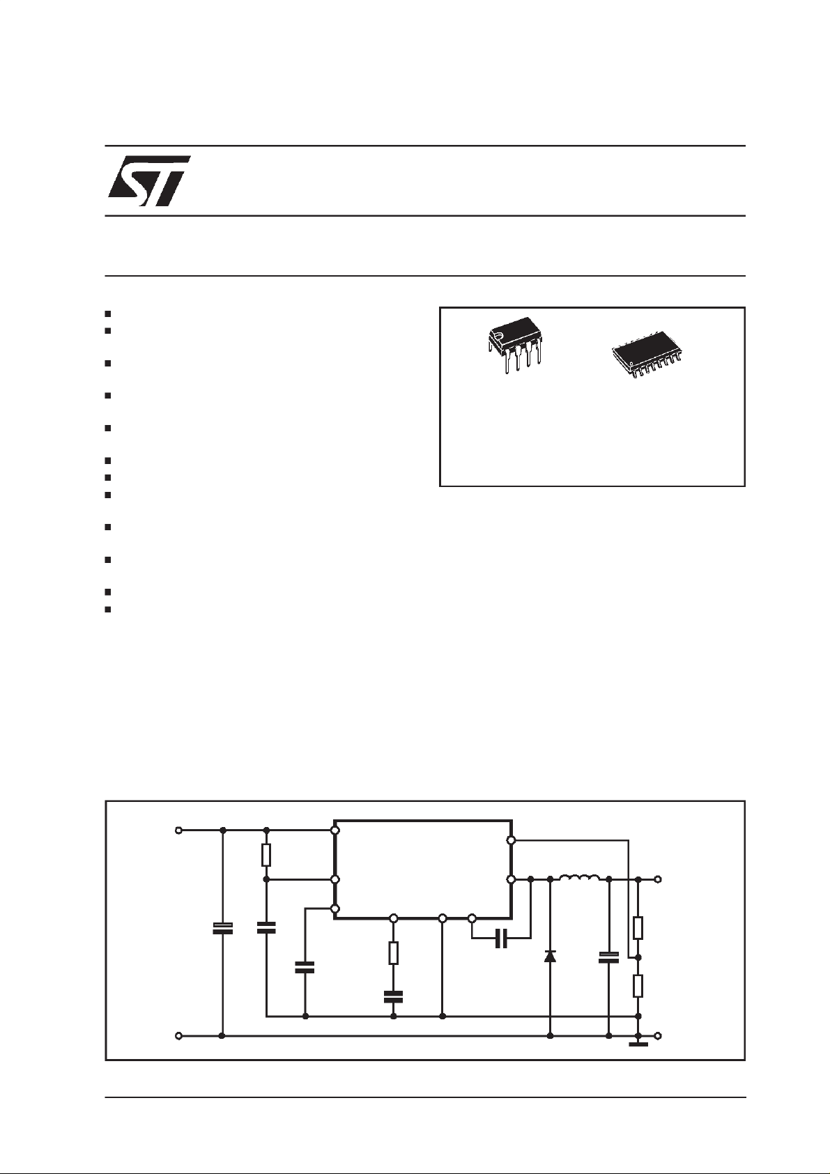
TYPICAL APPLICATIONCIRCUIT
L5971
Minidip
ORDERING NUMBERS: L5971 (Minidip)
A switching frequency up to 500KHz is achievable (the maximum power dissipation of the packages must be observed).
Features of this new generations of DC-DC converter include pulse-by-pulse current limit, hiccup
mode for short circuit protection, voltage feedforward regulation, soft-start, protection against
feedback loop disconnection, inhibit for zero current consumption and thermal shutdown.
The device is available in plastic dual in line,
MINIDIP 8 for standard assembly, and SO16 for
SMD assembly.
Typical Applications:
- High efficiencystep-downconverter
- Portable computers
- Batterycharger
- Distributedpower
- PDAsand MobileComminicators
SO16W
L5971D (SO16)
Vi=6V to 28V
May 2000
C1
47µF
30V
R1
22K
C2
1.2nF
C5
47nF
5(11)
3(4)
2(3)
7(13)
L5971
1(2)
R2
9.1K
C4
22nF
4(5,6)
6(12)
100nF
8(14)
C6
D98IN832C
D1
STPS
3L40U
L1
30µH
C
8
330µF
VO=2.5V/1.5A
R
3
R
4
1/11
L5971
BLOCKDIAGRAM
COMP
FB
2
7
8
1.26V
SS_INH
THERMAL
SHUTDOWN
INHIBIT SOFTSTART
E/A
OSCILLATOR
VOLTAGES
MONITOR
PWM
1.26V
INTERNAL
REFERENCE
R
Q
S
INTERNAL
SUPPLY
5.1V
DRIVE
VCC
5
CBOOT
CHARGE
CBOOT
CHARGE
AT LIGHT
LOADS
6
BOOT
3
OSC GND OUT
1
4
D98IN833
PIN CONNECTIONS
16
15
14
13
12
11
10
N.C.1
N.C.
FB
COMP
BOOT
VCC
N.C.
9
GND
SS_INH
OSC
OUT
1
2
3
4 VCC
D97IN595
FB8
COMP
7
BOOT
6
5
Minidip
N.C.
GND
SS_INH
OSC
OUT
OUT
N.C.
N.C. N.C.
2
3
4
5
6
7
8
D97IN596
SO16W
PIN FUNCTIONS
DIP SO (*) Name Function
1 2 GND Ground
2 3 SS_INH A logic signal (active low) disables the device (sleep mode operation).
3 4 OSC An external resistor connected between the unregulated input voltage and this pin and
4 5, 6 OUT Stepdown regulator output
511 V
CC
6 12 BOOT A capacitor connected between this pin and OUT allows to drive the internal VDMOS
7 13 COMP E/A output to be used for frequency compensation
8 14 FB Stepdown feedback input. Connecting directly this pin to the output 1.26V is obtained; a
(*) Pins 1, 7,8, 9, 10, 15 and 16 are not internally, electrically connected to the die.
A capacitor connected between this pin and ground determines the soft start time.
When this pin is grounded disables the device (driven by open collector/drain).
a capacitor connected from this pin to ground fix the switching frequency. (Line feed
forward is automatically obtained)
Not regulated DC input voltage
voltage divider is requested for higher output voltages
2/11
THERMALDATA
Symbol Parameter Minidip SO16 Unit
R
th(j-amb)
(*) Package mounted on board.
Thermal Resistance Junction to ambient Max. 90 (*) 110 (*) °C/W
ABSOLUTE MAXIMUM RATINGS
L5971
Symbol
Minidip S016
V
V
V
5,V3
V
4
I
4
6-V5
V
6
7,V2
V
8
V11,V4Input voltage 30 V
V5,V
I5,I
V12-V
V
12
V13,V
V
14
P
tot
Output DC voltage
6
Output peak voltage at t = 0.1µs f=200KHz
Maximum output current int. limit.
6
11
Bootstrap voltage 45 V
Analogs input voltage (VCC= 12V) 10 V
3
(VCC= 20V) 6
Power dissipation a T
Parameter Value Unit
-1
-5
V
V
14 V
V
-0.3
≤ 60°C Minidip 1W
amb
V
SO16 0.8 W
T
j,Tstg
Junction and storage temperature -40 to 150 °C
ELECTRICAL CHARACTERISTICS (Tj = 25°C, Cosc = 2.7nF, Rosc = 20kΩ,VCC = 12V, unless other-
wisespecified.) * SpecificationReferedto Tj from 0 to 125°C
Symbol Parameter Test Condition Min. Typ. Max. Unit
DYNAMICCHARACTERISTIC
V
I
V
o
V
d Dropout voltage Vcc = 10V; Io = 1.5A 0.44 0.55 V
I
l Maximum limiting current Vcc = 6.5 to 25V * 2 2.5 3 A
f
s Switching frequency * 90 100 110 KHz
SVRR Supply voltage ripple rejection V
Operating input voltage range * 6.5 28 V
Output voltage Io= 0.5A 1.247 1.26 1.273 V
I
= 0.2 to 1.5A 1.235 1.26 1.285 V
o
V
= 6.5to 25V * 1.21 1.26 1.31 V
cc
* 0.88 V
Efficiency V
Voltage stability of switching
o = 3.3V; Io = 1.5A 85 %
i =Vcc+2VRMS;Vo =Vref;
I
= 1.5A; f
o
ripple
= 100Hz
60 dB
Vcc = 6.5 to 25V 3 6 %
frequency
Temp. stability of switching
j = 0 to 125°C4%
T
frequency
Soft Start
Soft start charge current 30 40 50 µA
Soft start discharge current 6 10 14 µA
Inhibit
VLL Low level voltage * 0.9 V
I
sLL Isource Low level * 5 15 µA
3/11
L5971
ELECTRICAL CHARACTERISTICS (continued)
Symbol Parameter Test Condition Min. Typ. Max. Unit
DC Characteristics
Iqop Total operating quiescent
current
I
q Quiescent current Duty Cycle = 0; V
I
qst-by
Total stand-by quiescent
current
Error Amplifier
V
FB
R
L Line regulation Vcc = 6.5 to 25V 5 10 mV
V
oH High level output voltage V
V
oL Low level output voltage V
I
o source Source output current V
I
o sink Sink output current V
I
b Source bias current 2 3 µA
SVRR E/A Supply voltage ripple rejection V
gm Transconductance I
Voltage Feedback Input 1.247 1.26 1.273 V
Ref. voltage stability vs
temperature
DC open loop gain R
OscillatorSection
Ramp Valley 0.74 0.81 0.88 V
Ramp peak Vcc= 6.5V 1.80 1.87 1.94 V
Maximum duty cycle 95 97 %
Maximum Frequency Duty Cycle = 0%
Pin 5 (Pin 11) 3 4.5 mA
= 1.7V 2.8 3.5 mA
FB
V
<0.9V 100 200 µA
inh
Vcc = 25V; V
<0.9V 150 300 µA
inh
* 0.4 mV/°C
= 0.8V 8.7 V
FB
= 1.7V 0.65 V
FB
= 3V; VFB= 0.8V 180 250 µA
comp
= 3V; VFB= 1.7V 200 300 µA
comp
comp=Vfb
L
comp
V
comp
; Vcc = 6.5 to 25V 60 80 dB
= ∞ 50 57 dB
= -0.1 to 0.1mA
4.3 mS
=6V
Vcc = 25V 4.72 4.79 4.86 V
500 kHz
R
= 13kΩ,C
osc
= 820pF
osc
4/11

Figure1. Testand valutation board circuit.
L5971
Vi=6V to 28V
C1
47µ
30V
R
1
22K
C
F
1.2nF
2
5(11)
7(13)
L5971
R
2
9.1K
C
22nF
3(4)
2(3)
C
5
47nF
8(14)
4(5,6)
6(12)
1(2)
C
6
STPS
3L40U
D98IN832C
D1
100nF
4
Figure2. PCBand componentlayout of the figure 1.
L1
30µH
C
330µF
VO(V) R3 (KΩ)R4(KΩ)
V
=2.5V/1.5A
O
1.8 1 2
1.5 0.5 2
R
3
8
R
4
2.5 2 2
3.3 8.2 4.7
5.1 12 3.6
12 27 3
15 23 2
SOLDER SIDE
COMPONENT SIDE
5/11

L5971
Figure3. Quiescentdraincurrent vs. input
voltage.
Iq
(mA)
5
200KHz
R1=22K
C2=1.2nF
4
3
100KHz;
R1=20K
C2=2.7nF
0Hz
2
1
0 5 10 15 20 25
D98IN942
Tamb=25°
0% DC
C
Vcc(V)
Figure5. Stand-bydrain currentvs. input
voltage
Ibias
(µA)
150
Vss=GND
140
130
120
110
Tj=25°C
100
90
80
70
60
0 5 10 15 20 25 VCC(V)
D98IN944
Tj=125°C
Figure7. Switchingfrquency vs. R1 and C2
fsw
(KHz)
500
D97IN784
Tamb=25°C
Figure 4. Quiescent current vs. junction
temperature
V
CC
0% DC
=2.7nF
2
D98IN943
=20V
Iq
(mA)
5
4
3
200KHz; R
100KHz;
R
=20K;
1
=22K; C2=1.2nF
1
C
0Hz
2
1
-50 -30 -10 10 30 50 70 90 110 Tj(°C)
Figure 6. LineRegulation
VO
(V)
3.377
3.376
3.375
Tj=125°C
3.374
3.373
3.372
3.371
3.370
0 5 10 15 20 25 VCC(V)
D98IN945
Tj=25°C
Figure 8. Switching Frequency vs. input
voltage.
fsw
(KHz)
107.5
D98IN947
6/11
200
0.82nF
1.2nF
100
50
20
2.2nF
3.3nF
4.7nF
5.6nF
10
5
0 20 40 60 80 R1(KΩ)
105.0
102.5
Tj=25°C
100.0
97.5
95.0
92.5
90.0
0 5 10 15 20 25 VCC(V)

L5971
Figure9. Switchingfrequency vs. junction
temperature.
fsw
(KHz)
105
100
95
90
-50 0 50 100 Tj(°C)
D97IN785
Figure11. Efficiency vs output voltage.
(%)
96
94
92
90
88
86
84
η
100KHz
200KHz
V
I
O
CC
=1.5A
D98IN948
=20V
Figure 10. Dropout voltage between pin 5
and 4.
∆V
(V)
0.5
0.4
0.3
0.2
0.1
0.0
0.0 0.2 0.4 0.6 0.8 1.0 1.2 1.4 IO(A)
D97IN736
Tj=125°C
Tj=25°C
Tj=-25°C
Figure 12. Efficiency vs. output current.
η
(%)
90
85
80
=12V
V
CC
V
=18V
CC
fsw=200KHz
VO=5.1V
D98IN949
VCC=8V
82
0 5 10 15 20 25 VO(V)
Figure13. Efficiency vs output current.
η
(%)
90
85
V
CC
=12V
V
CC
VCC=8V
=18V
80
75
0.0 0.2 0.4 0.6 0.8 1.0 1.2 1.4 IO(A)
D98IN950
fsw=200KHz
VO=3.36V
75
0 0.2 0.4 0.6 0.8 1.0 1.2 1.4 IO(A)
Figure 14. Efficiency vs. output current.
η
(%)
90
85
80
75
Vcc=8V
Vcc=12V
Vcc=18V
70
65
60
0 0.2 0.4 0.6 0.8 1.0 1.2 1.4 Io(A)
D98IN941
Fsw=200KHz
Vo=2.5V
7/11

L5971
Figure 15. Load transient.
Figure17. Soft start capacitorselectionvs. In-
ductor and V
L
(µH)
150
ccmax
D98IN953
fsw=200KHz
Figure 16. Soft start capacitorselection vs. In-
ductorand V
L
(µH)
160
120
80
40
0
fsw=100KHz
20 22 24 26 28
ccmax
680nF
D98IN952
470nF
330nF
220nF
100nF
V
CCmax
(V)
Figure 18. Open loop frequencyand phase of
erroramplifier.
GAIN
(dB)
50
0
GAIN
D97IN787
Phase
0
100
50
0
20 22 24 26 28 V
56nF
47nF
33nF
22nF
CCmax
(V)
-50
-100
-150
-200
10 10
45
90
Phase
135
3
2
10
5
4
10
10
7
6
10
10
8
f(Hz)10
8/11

L5971
DIM.
MIN. TYP. MAX. MIN. TYP. MAX.
A 3.32 0.131
a1 0.51 0.020
B 1.15 1.65 0.045 0.065
b 0.356 0.55 0.014 0.022
b1 0.204 0.304 0.008 0.012
D 10.92 0.430
E 7.95 9.75 0.313 0.384
e 2.54 0.100
e3 7.62 0.300
e4 7.62 0.300
F 6.6 0.260
I 5.08 0.200
L 3.18 3.81 0.125 0.150
Z 1.52 0.060
mm inch
OUTLINE AND
MECHANICAL DATA
Minidip
9/11

L5971
DIM.
MIN. TYP. MAX. MIN. TYP. MAX.
A 2.35 2.65 0.093 0.104
A1 0.1 0.3 0.004 0.012
B 0.33 0.51 0.013 0.020
C 0.23 0.32 0.009
D 10.1 10.5 0.398 0.413
E 7.4 7.6 0.291 0.299
e 1.27 0.050
H 10 10.65 0.394 0.419
h 0.25 0.75 0.010 0.030
L 0.4 1.27 0.016 0.050
K0°(min.)8° (max.)
mm inch
0.013
OUTLINE AND
MECHANICAL DATA
SO16 Wide
L
hx
45
A
B
e
K
A1
C
H
D
16
9
E
1
8
10/11

L5971
Information furnished is believed to be accurate and reliable. However, STMicroelectronics assumes no responsibility for the consequences
of use of such information nor for any infringement of patents or other rights of third parties which may result from its use. No license is
granted by implication or otherwise under any patent or patent rights of STMicroelectronics. Specification mentioned in this publication are
subject to change without notice. This publication supersedes and replaces all information previously supplied. STMicroelectronics products
are not authorized for use as critical components in life support devices or systems without express written approval of STMicroelectronics.
The ST logo is a registered trademark of STMicroelectronics
2000 STMicroelectronics – Printedin Italy – All Rights Reserved
STMicroelectronics GROUP OF COMPANIES
Australia - Brazil - China - Finland- France - Germany - Hong Kong - India - Italy - Japan - Malaysia - Malta - Morocco -
Singapore- Spain - Sweden - Switzerland - United Kingdom - U.S.A.
http://www.st.com
11/11
 Loading...