

UP TO 1A STEP DOWN SWITCHING REGULATOR
■ UP TO 1A OUTPUT CURRENT
■ OPERATING INPUT VOLTAGE FROM 4.4V
TO 36V
■ 3.3V / (±2%) / REFERENCE VOLTAGE
■ OUTPUT VOLTAGE ADJUSTABLE FROM
1.2V TO 35V
■ LOW DROPOUT OPERATION: 100% DUTY
CYCLE
■ 250KHz INTERNALLY FIXED FREQUENCY
■ VOLTAGE FEEDFO RWA R D
■ ZERO LOAD CURRENT OPERATION
■ INTERNAL CURRENT LIMITING
■ INHIBIT FOR ZERO CURRENT
CONSUMPTION
■ SINCHRONIZATION
■ PROTECTION AGAINST FEEDBACK
DISCONNECTION
■ THERMAL SHUTDOWN
APPLICATIONS:
■ CONSUMER: STB, DVD, TV, VCR,CAR
RADIO, LCD MONITORS
■ NETWORKING: XDSL, MODEMS,DC-DC
MODULES
■ COMPUTER: PRINTERS, AUDIO/GRAPHIC
CARDS, OPTICAL STORAGE, HARD DISK
DRIVE
■ INDUSTRIAL: CHARGERS, CAR BATTERY
DC-DC CONVERTERS
L5970D
SO8
ORDERING NUMBERS: L5970D (SO8)
L5970D013TR (T&R)
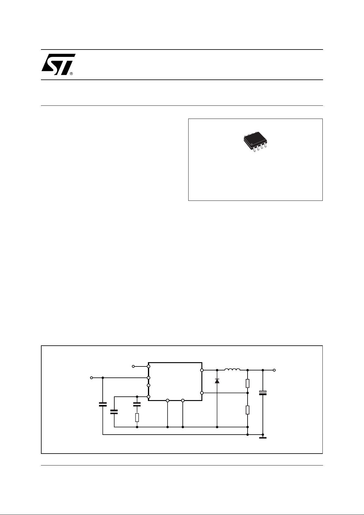
DESCRIPTION
The L5970D is a step down monolithic power
switching regulator capable to deliver up to 1A at
output voltages from 1.2V to 35V.
The device uses an internal P-Channel D-MOS
transistor (with a typical Rdson of 250mΩ) as
switching element to mi nimize the size of the external components.
An internal oscillator fixes the switching frequency
at 250KHz.
Having a minimum inpu t vol tage of 4. 4V only, it is
particularly suitable for 5V bus, available in all
computer related applications.
Pulse by pulse current limit with the internal frequency modulation offers an effective constant
current short circuit protection.
TEST APPLICATION CIRCUIT
3.3V
VIN = 4.4V to 35V
C1
10µF
35V
CERAMIC
May 2003
22nF
220pF
C4
C3
VREF
VCC
SYNC.
COMP
R3
4.7K
6
8
2
4
INH.
L5970D
3
7
1
5
GND
D98IN954C
OUT
FB
L1 33µH
D1
STPS2L40U
R1
5.6K
R2
3.3K
VOUT=3.3V
C2
100µF
10V
1/10
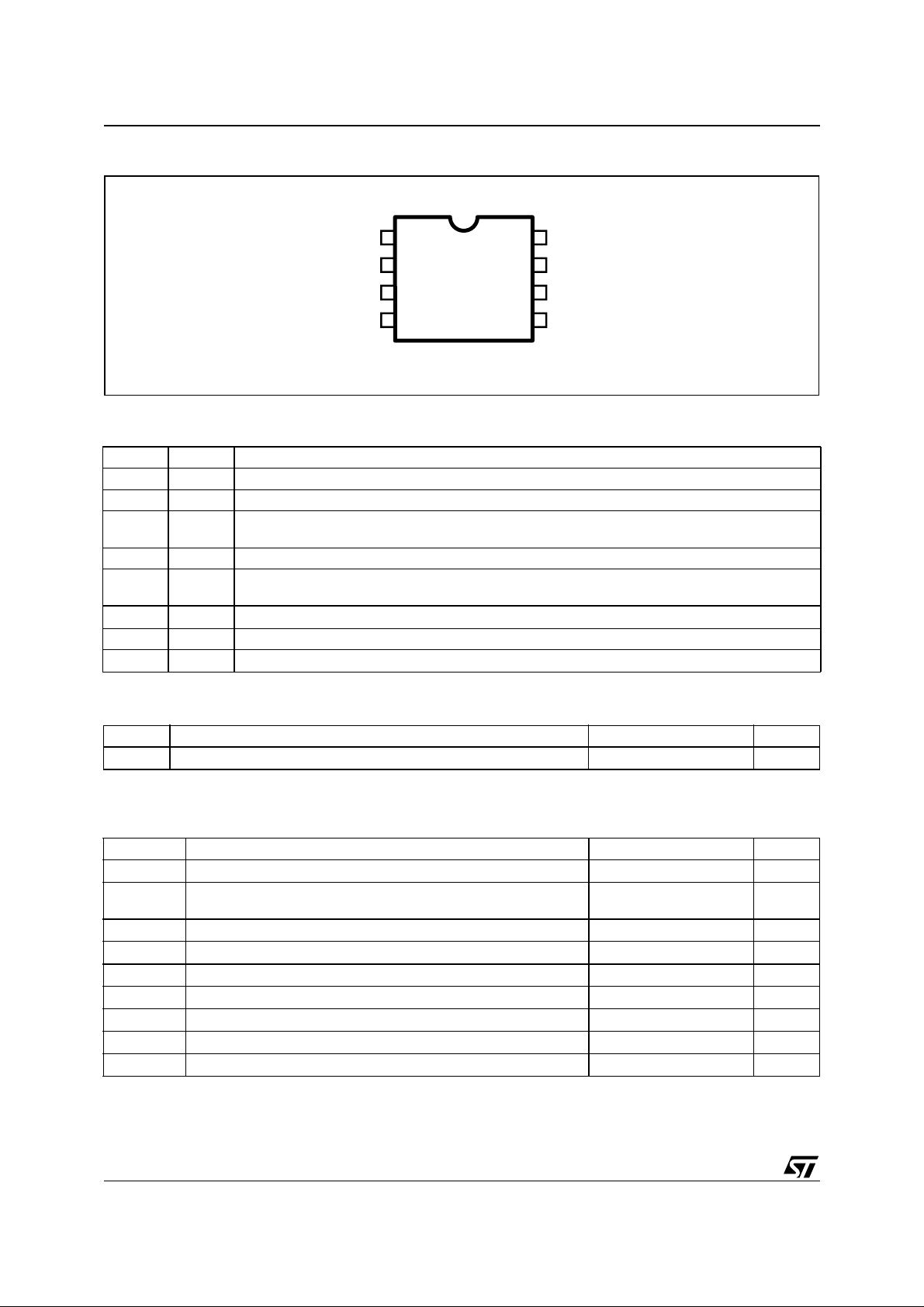
L5970D
PINS CONNECTION (Top View)
OUT
SYNC
INH
COMP
1
2
3
4
8
7
6
5
D98IN955
VCC
GND
VREF
FB
PINS FUNCTION
N. Name Description
1 OUT Regulator Output.
2 SYNC Master/slave synchronization.
3 INH A logical signal (active high) disables the device. If INH not used the pin must be grounded.
When it is open an internal pull-up disable the device.
4 COMP E/A output for frequency compensation.
5 FB Feedback input. Connecting directly to this pin results in an output voltage of 1.23V. An external
resistive divider is required for higher output voltages.
6V
7 GND Ground.
8V
3.3V V
REF
Unregulated DC input voltage.
CC
. No cap is requested for stability.
REF
THERMA L D ATA
Symbol Parameter Value Unit
R
th (j-amb)
(*) Package mounted on board
Thermal Resistance Junction to ambient Max. 120 (*) °C/W
ABSOLUTE MAXIMUM RATINGS
Symbol Parameter Value Unit
V
V
I
1
, V
V
4
V
V
P
tot
T
T
stg
Input Voltage 40 V
8
Output DC voltage
1
Output peak voltage at t = 0.1µs
-1 to 40
-5 to 40
Maximum output current int. limit.
Analog pins 4 V
5
INH -0.3V to V
3
SYNC -0.3 to 4 V
2
Power dissipation at T
Operating junction temperature range -40 to 150 °C
j
≤ 60°C 0.75 W
amb
Storage temperature range -55 to 150 °C
CC
V
V
2/10
L5970D
ELECTRICAL CHARACTERISTCS (Tj = 25°C, VCC = 12V, unless otherwise specified.)
(*) Specification Referred to T
Symbol Parameter Test Condition Min. Typ. Max. Unit
V
DYNAMIC CHARACTERISTICS (see test circuit fig. xx note 1).
DC CHARACTERISTICS
I
I
qst-by
INHIBIT
ERROR AMPLIFIER
V
V
I
o source
I
o sink
gm Transconductance I
SYNC FUNCTION
REFERENCE SECTION
Note (1): S pecification over the -40 to +125 Tj Temperature range are ass ured by design, characte ri zation and statistical correlation.
Note (2): Guar anteed by design.
Operating input voltage
CC
range
Dropout voltage VCC = 4.4V; Io = 1A * 0.25 0.5 V
V
d
I
Maximum limiting current VCC = 4.4V to 36V * 1.5 1.87 2.25 A
l
fs Switching frequency * 212 250 280 KHz
Duty cycle 0 100 %
V
Voltage feedback 4.4V < VCC < 36V,
5
η Efficiency VO = 5V, VCC = 12V 90 %
Total operating quiescent
qop
current
Quiescent current Duty Cycle = 0; VFB = 1.5V 2.5 mA
I
q
Total stand-by quiescent
current
INH Threshold voltage Device ON 0.8 V
High level output voltage VFB = 1V 3.5 V
OH
Low level output voltage VFB = 1.5V 0.4 V
OL
Source output current V
Sink output current V
I
Source bias current 2.5 4 µA
b
DC open loop gain R
High Input Voltage V
Low Input Voltage V
Slave Sink Current
Master Output Amplitude I
Output Pulse Width no load, V
Reference Voltage 3.234 3.3 3.366 V
Line Regulation I
Load Regulation I
Short Circuit Current 10 8 30 mA
from -40 to +125°C (1).
j
Vo = 1.235V; Io = 1A * 4.4 36 V
20mA < IO < 1A
V
> 2.2V
inh
VCC = 36V; V
> 2.2V
inh
Device OFF 2.2 V
= 1.9V; VFB = 1V 200 300 µA
COMP
= 1.9V; VFB = 1.5V 1 1.5 mA
comp
= ∞ 50 65 dB
L
= -0.1mA to 0.1mA
comp
V
= 1.9V
comp
= 4.4V to 36V 2.5 V
CC
= 4.4V to 36V 0.74 V
CC
= 0.74V
V
sync
V
= 2.33V
sync
= 3mA 2.75 3 V
source
I
= 0 to 5mA
REF
(2)
= 1.65V 0.20 0.35 µs
sync
VCC = 4.4V to 36V
= 0mA
REF
V
= 4.4V to 36V
CC
= 0 to 5mA 8 15 mV
REF
225 250 275 KHz
1.220 1.235 1.25 V
* 1.198 1.235 1.272 V
*35mA
*
*
50
80
100
150
2.3 mS
REF
0.11
0.21
0.25
0.45
* 3.2 3.3 3.399 V
510mV
µA
µA
V
mA
mA
3/10

L5970D
Figure 1. Junction Temperature vs. Output
Current (SO8) *)
Tj(°C)
130
120
110
100
90
80
Vcc=5V
Tamb=25°C
Vo=3.3V
Vo=2.5V
Vo=1.8V
70
60
50
40
30
20
0.2 0.4 0.6 0.8 1 1.2 1.4 1.6
Io(A)
Figure 2. Junction Temperature vs. Output
Current (SO8) *)
Tj(°C)
130
120
110
100
90
80
70
60
50
40
30
20
Vcc=12V
Tamb=25°C
0.20.40.60.8 1 1.21.41.6
Io(A)
Vo=5V
Vo=3.3V
Vo=2.5V
Figure 3. Junction Temperature vs. Output
Current (SO8) *)
Tj(°C)
140
Vo=18V
120
100
Vcc=24V
Tamb=25°C
80
60
40
20
0
0.2 0.4 0.6 0.8 1 1.2 1.4
Io(A)
Vo=12V
Vo=5V
Figure 4. Loa d R egulation
Vo (V)
3.312
3.308
Vcc = 12V
Vo = 3.3V
3.304
3.3
Tj = 25°C
3.296
3.292
3.288
3.284
Tj = 125°C
3.28
3.276
00.511.5
Io (A)
Figure 5. Line R egulation
Vo (V)
3.312
3.304
Vcc = 12V
Vo = 3.3V
Tj = 25°C
3.308
3.3
3.296
3.292
3.288
Tj = 125°C
3.284
3.28
3.276
010203040
Vcc (V)
Figure 6. Out put V ol t age v s. Junction
Temperature
Vo (V)
1.25
1.24
1.23
1.22
Vcc = 12V
1.21
Vcc=12V
1.2
-50 0 50 100 150
Tj (°C)
*) Package mounted on demoboard
4/10

L5970D
Figure 7. Quiescent Current vs. Junction
Temperature
Iq (mA)
2
1.8
1.6
Vcc = 12V
1.4
DC = 0%
1.2
-50
050
100 150
Tj (°C)
Figure 8. Shutdown Curr ent vs. J un ct io n
Temperature
Ishd (µA)
70
60
Vcc = 12V
Figure 9. Switching Frequency vs.Junction
Temperature
Fsw (KHz)
260
250
240
230
220
-50 0 50 100 150
Vcc = 12V
Vo = 3.3V
Tj (C)
50
40
30
-50
0
50 100 150
Tj (°C)
5/10

L5970D
Figure 10. Demoboard schematic
VIN = 4.4V to 25V
C1
10µF
25V
CERAMIC
3.3V
C4
22nF
C3
220pF
VREF
VCC
SYNC.
COMP
4.7K
R3
6
8
2
4
INH.
L5970D
3
7
1
5
GND
D03IN1437
OUT
FB
L1 33µH
D1
STPS2L25U
R1
5.6K
R2
3.3K
Part list demoboard
Reference Part Number Description Manufacturer
C1 10µF, 25V TOKIN
C2 POSCAP 10TPB100M 100µF, 10V Sanyo
C3 C1206C221J5GAC 220pF, 5%, 50V KEMET
C4 C1206C223K5RAC 22nF, 10%, 50V KEMET
VOUT=3.3V
C2
100µF
10V
R1 5.6K, 1%, 0.1W 0603 Neohm
R2 3.3K, 1%, 0.1W 0603 Neohm
R3 4.7K, 1%, 0.1W 0603 Neohm
D1 STPS2L25U 2A, 25V STMicroelectronics
L1 DO3316P-333 33µH, 2A COILCRAFT
Figure 11. Efficiency vs. Output Current Figure 12. Efficiency vs. Output Current
94
92
90
88
86
84
82
80
Efficiency (%)
78
76
74
Vcc=5V
72
70
0.1 0.2 0.3 0.4 0.5 0.6 0.7 0.8 0.9 1
Vo=3.3V
Vo=2.5V
Vo=1.8V
Io (A)
92
90
88
86
84
82
80
78
Efficiency (%)
76
74
72
70
0.1 0.2 0.3 0.4 0.5 0.6 0.7 0.8 0.9 1
Vo=5V
Vo=3.3V
Vo=2.5V
Vcc=1 2 V
Io (A)
6/10

Figure 13. PC B layout (comp on e nt s id e)
Figure 14. PCB layout (bottom side)
L5970D
42mm
34mm
Figure 15. PC B layout (front si de)
7/10

L5970D
APPLICATION IDEAS
Figure 16. Dua l ou t put v ol tage with auxili ary wi nding
N1/N2=2
D2
1N4148
VOUT1=5V
30mA
VIN=12V
C1
10uF
25V
Ceramic
C2
220pF
C3
22nF
R3
4.7k
VCC
COMP
SYNC VREF
8
4
2
Figure 17. Buck-Boost regulator
VIN=12V
C1
10uF
25V
Ceramic
Vin=12V Vout= -12 V Iout= 0.5A Efficiency=81%
C2
10uF
35V
Ceramic
C3
220pF
C4
22nF
R3
4.7k
VCC
COMP
SYNC
Figure 18. Positive Buck-Boost regul
VIN=5V
C1
10uF
25V
Ceramic
C2
220pF
C3
22nF
R3
4.7k
VCC
COMP
SYNC VREF
8
U1
L5970
4
6
2
3.3V
U1
L5970D
6
GND
3.3V
8
4
2
7
GND
VREF
7
U1
L5970
6
3.3V
1
5
3
INH
1
5
3
GND
OUT
FB
OUT
FB
INH
7
1
5
3
INH
D1
STPS2L25U
D1
STPS25L25U
OUT
FB
24k
L1
33uH
2.7k
Lp=22uH
L1
33uH
D1
STPS2L25U
C5
100uF
16V
D2
STPS2L2 5U
M1
STN4NE03L
C4
100uF
10V
VOUT=-12V/0.3A
24k
2.7k
VOUT=3.3V
0.5A
C5
47uF
10V
VOU T=1 2V/0.3 A
C4
100uF
16V
Vin=5V Vout=12V Iout=0.3A Efficiency=76%
Figure 19. Sy nchroniza tion example
VIN
VCC
8
COMP
4
SYNC VREF
8/10
2
L5970D
6
GND
OUT
VCC
COMP
8
4
2
SYNC VREF
L5970D
6
GND
1
FB
5
3
7
INH
OUT
1
FB
5
3
7
INH

L5970D
DIM.
D (1) 4.8 5.0 0.189 0.197
F (1) 3.8 4.0 0.15 0.157
(1) D and F do not include mold flash or protrusions. Mold flash or
potrusions shall not exceed 0.15mm (.006inch).
MIN. TYP. MAX. MIN. TYP. MAX.
A 1.75 0.069
a1 0.1 0.25 0.004 0.010
a2 1.65 0.065
a3 0.65 0.85 0.026 0.033
b 0.35 0.48 0.014 0.019
b1 0.19 0.25 0.007 0.010
C 0.25 0.5 0.010 0.020
c1 45° (typ.)
E 5.8 6.2 0.228 0.244
e 1.27 0.050
e3 3.81 0.150
L 0.4 1.27 0.016 0.050
M 0.6 0.024
S8° (max.)
mm inch
OUTLINE AND
MECHANICAL DATA
SO8
9/10

L5970D
Information furnished is believed to be accurate and reliable. However, STMicroelectronics assumes no responsibility for the consequences
of use of such information nor for any infringement of patents or other rights of third parties which may result from its use. No license is granted
by implic ation or otherwise under any patent or patent ri ghts of STM i croelectronics. Specificat i ons menti oned in thi s publication are subject
to change without notice. This publication supersedes and replaces all information previously supplied. STMicroelectronics product s are not
authoriz ed f or use as crit i cal compone nts in life support devices or systems wi thout express written approval of STMicroel ectronics.
STMicroelectronics acknowledges the trademarks of all companies referr ed to in this document.
The ST logo is a registered trademark of STMicroelectronics
©
2003 STMicroelectronics - All Ri ghts Rese rved
Austra lia - Brazil - Canada - Chi na - F inland - Fr ance - Germa ny - Hong Kong - India - Israel - Italy - Japa n -M alaysia - Malta - Morocco -
Singap ore - Spain - Sw eden - Switze rl and - Unit ed K ingdom - Uni ted States .
STMicroelectronics GROUP OF COMPANIES
http://www.s t. com
10/10
 Loading...