

L5951
TRIPLE OUTPUT MULTIFUNCTION VOLTAGE REGULATOR
FOR CAR RADIO WITH IDR/CLASS 2 INTERFACE
■
3 VOLTAGE REGULATORS:
3.3V (100mA) STANDBY REGULATOR
5V (100mA) STANDBY REGULATOR
7.8V (100mA)
■
OUT OF REGULATION DETECTION FOR 5VSTANDBY REGULATO R
■
WIDE OPERATING SUPPLY VOLTAGE
RANGE FROM 4.5V UP TO 26.5V FOR
TRANSIENT 34V
■
VERY LOW STANDBY QUIESCENT
CURRENT (<150µA)
■
INPUT TO OUTPU T SIGNAL T RANS FER
FUNCTION PROGRAMM AB LE
■
LVS FUNCTION
■
TTL AND CMOS COMPATIBLE INPUTS
■
OUTPUT CURRENT LIMITATION
■
CONTROLLED OUTPUT SLOPE FOR LOW
EMI
■
OVERTEMPERATURE SHUT-DOWN
■
ABLE TO SURVIVE UNDER LOSS OF
ORDERING NUMBER: L5951
GROUND OR BATTERY
■
ESD PROTECTED
DESCRIPTION
The L5951 is a monolithic triple regulator integrated
with a SAE J1850 Integrated Driver / Receiver realized in advanced Multipower-BCD technology. It is
intended to drive single wire J1850 communications,
and offer microcontroller power and power management for automotive or industrial applications.
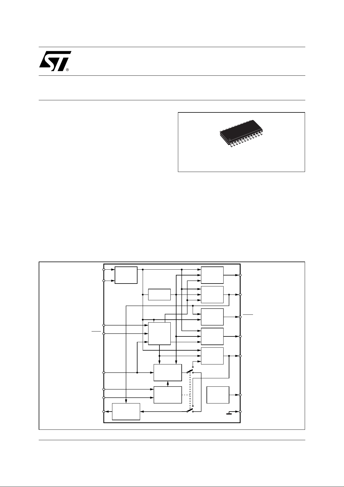
SO24
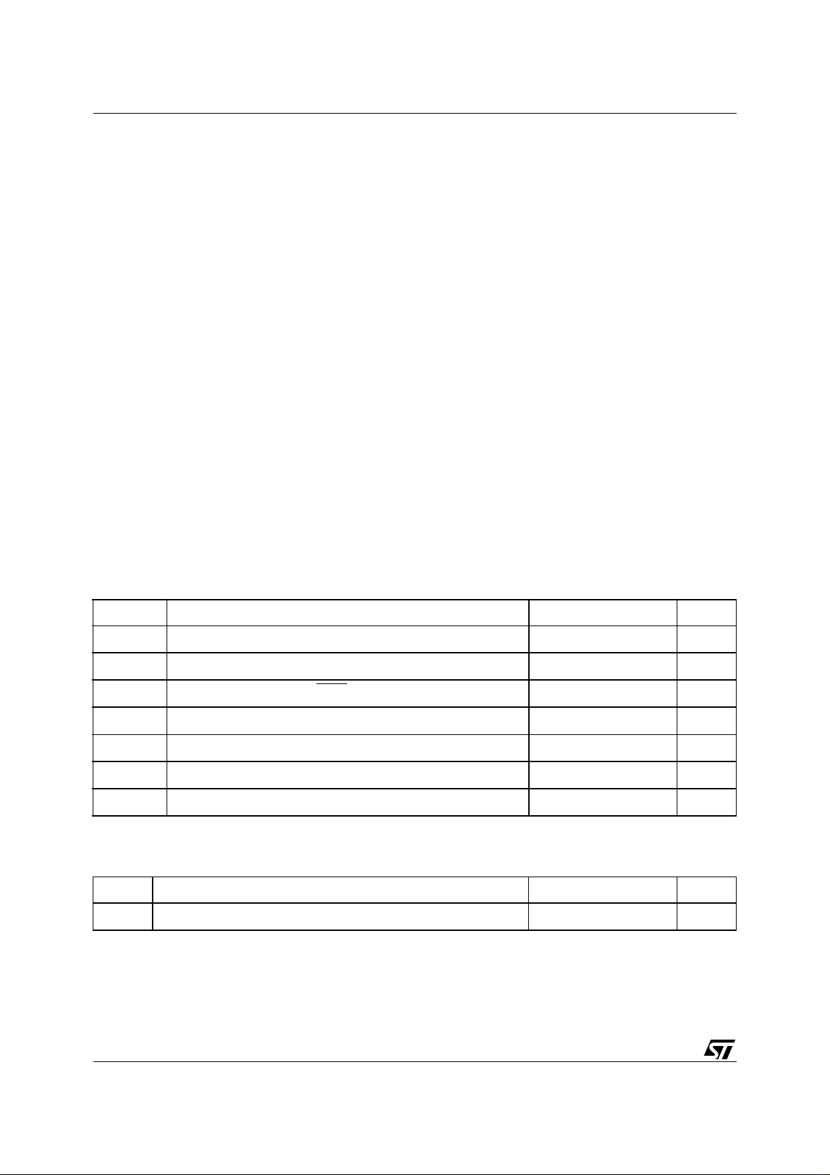
BLOCK DIAGRAM
VBAT
LVS
SLEEP
LOOP
EN
TX
4X
RX
SUPPLY
SELECTOR
DIGITAL OUTPUT
DRIVER
BANDGAP
REFERENCE
ENABLE/
PROTECTION
LOGIC
WAVESHAPING
FILTER
4XEN AND
LOOPBACK
3V
STANDBY
5V
STANDBY
RESET
7.8V
BUS DRIVER
LOSS
OF GND
PROTECTION
REG1
REG2
RESET
REG3
BUS
LOAD
GND
D99AU991
January 2001
1/13

L5951
1 FUNCTIONAL DESCRIPTION
1.1 General Features
The L5951 is an integrated circuit which provides a J1850 physical layer as well three voltage regulators. The
L5951 was developed to provide the power and Class 2/IDR interface for a microcontroller.
1.2 REG1 Outp ut Voltage
The REG1 regulator output is equal to 3.3V. The 3.3V regula tor i s non low drop out and can handl e cur rents up
to 100mA with short citcuit limit of 280mA.
1.3 REG2 Outp ut Voltage
The REG2 regulator output is equal to 5V and can handle curr ents up to 100mA with short c itcuit limit of 280mA.
The output stage of the 5V regulator is low dropout.
1.4 REG3 Outp ut Voltage
The REG3 regulator output is equal to 7.8V and can handle currents up to 100mA with short citcuit limit of
280mA. The output stage of the 7.8V regulator is low dropout. REG3 regulator is controlled by the EN (enable)
pin of the IC. REG3 can be turned on and off by toggling the EN pin. A logic "1" on the EN pin enables REG3,
while a logic "0" on the EN pin disables REG3. The maximum voltage when REG3 is off must be less than 0.2V.
Sleep* Input -
is above 2VDC, the transmitter is enabled. If the Sleep* pin drops below 0.8VDC, and EN is "0" the transceiver
goes into a low power mode. In low power mode, REG3 and the transceiver are disabled. The L5951 will still
receive messages and send them to the microcontroller out of the RX pin.
LVS input -
thermal shutdown at high voltage. For this reason a sec ondary low voltage s upply (LV S) can be used to r educe
power dissipation.
Reset* Output -
REG2 drops 0.3VDC below its normal operating voltage, the Reset* pin will go to a logic "0". Between the voltage levels of 4.65VDC (min) and 5.10VDC (max) on REG2, a reset will occur. There is a hysterisis of 50mV on
the Reset* pin.
Low Input Voltage Operation -
ready for the return of normal voltage battery levels. The L5951 will be able to retrieve data off the BUS and
send it to the micrprocessor when the supply voltage is as low as 4.9V. The regulators should stay the same
voltage as the battery voltage down to 7.0V minus operati ng headroom for the 7.8V regulator . BUS V
not guaranteed over all conditions below VBAT = 9.0V.
Waveshaping -
The digital signal is rounded at the switching points in order to reduce EMI emissions. A second order function,
I = C*dV/dt, is used to control the rise and fall times of the transmission. The rise and fall times are controlled
by an external resistor Rext . The waveshaping circuit can be enabled and disabled by the 4X pin. A logic "1"
will disable the waveshape circuit and a logic "0" will enable the waveshape circuit. In 4X mode, the speed of
the BUS is increased by a factor of four . Any signal coming from the microcontroller and going to the BUS must
be waveshaped. If loopback(LOOP) is enabled, the signal coming from the micro through the TX pin is routed
to the RX pin back to the micro with or without it being waveshaped. A logic "1" enabl es loop back and a logi c"0"
disables loopback.
Nodes -
waveforms and transmi ts a digital level signal back to a l ogic IC. The trans mitter can drive up to 32 remote transceivers. These remote nodes may be at ground potentials that ar e ±2 VDC, with respect to the assembly. Under
this condition, waveshaping will only be maintained during 3 of the 4 corners. The L5951 is a remote node on
the Class 2/IDR Bus. Each remote transcei ver has a 470 + 10% pF c apacitor on its output for EMI suppression,
The Class 2 transmitter can be turned on and turned off by the Sleep* pin. Once the voltage level
* denote s ac tive low
Reg1 and Reg2 are supplied by Vbat pin. The device could then dissipate a lot of power, causing
The L5951 has low voltage or no voltage circuitry that is a warning to the microcontroller. If
* denote s ac tive low
If battery voltage level drops below 7.0V, the outputs are to remain alive and
are
OH,min
Messages sent by the microcontroller to the transceiver are routed to a waveshaping circuit.
The transmitter provides a wave-shaped 0 to 7.7 VDC waveform on the BUS output. It also receives
2/13

L5951
as well as a 10.6 kW + 5% pull down resistor to ground. The main node has a 3,300 + 10% pF capacitor on its
output for EMI suppression, as well as a 1.5 k
there is no pr imary node , all nodes will have the 470 ±10% pF cap acitor and the 10.6k
No matter how many remote nodes are on the Class 2/IDR Bus, the RC of the Class 2/IDR Bus is maintained
at approximately 5ms. The minimum and maximum load on the Class 2/IDR Bus is given below :
Minimum Nodes (3.33 · .9) + (.47 · .9) = 3.39 nF (1.5 · 1.05) || (10.6 · 1.05) = 1.38 kΩ
Maximum Nodes (3.3 · 1.1) + 25·(0.47 · 1.1) = 16.55 nF (1.5 · 0.95) || (10.6 · 0.95) / 25 = 314Ω
1.5 Protection
The L5951 can survive under the following conditions: shorting the outputs to BAT and GND, loss of BAT, loss
of IC GND, double battery(+26.5V), 4000V ESD, 34V load dump. L5951 will not handle a reverse battery condition. External components must be implemented for reverse battery protection.
Thermal Shutdown:
thermal shutdown is broken down into two areas; V1 and V2 ouputs, and the other is V3
output and the Class 2 Bus Driver. V1 and V2 outputs shutdown at 160°C and returns to normal operation at
130°C. The V3 output and Class 2 Bus Driver shutdown at 150°C and return to normal operation at 120°C.
Current Limiting:
each voltage regulator w ill contain its ow n current prote ction, and the max imum al lowable cur -
rent for all three regulators is 280mA.
Short Circuit:
If the outputs are short circuited, the IC will begin current limi ting and eventually the thermal shut-
down will kick in. Current limiting will not disable the outputs.
Overvoltage:
The IC will not operate if the BAT voltage reaches 30V or above. V1 and V2 will not be shutdown,
but all other outputs will not operate.
Loss of Ground & Loss of Battery Connection:
Ω
+ 5% pull down resistor to ground. With more than 26 nodes
Ω ±
5% pull down resistor.
Capacitance Resistance to Ground
in this conditions a very small leakage on BUS is generated.
1.6 Protocol Description
The L5951 uses a Variable Pulse Width (VPW) modulated protocol. One frame consists of an entire message
not containing more than 12 bytes. The first bi t of each byte w ill b e the most sign ificant bi t (MSB). A transm itted
message begins with a SOF signal and ends with the EOF signal.
The data to be transmitted has to be in a specific format as follows:
idle,SOF,DATA, CRC, EOD , NB, IFR, EOF, IFS, idle
Definitions below:
idle: Logic level low on communication bus
SOF: Start of Frame
DATA: Data Bytes
CRC: Cyclic Redundancy Check Error Detection Byte
EOD: End of DATA(only when IFR is used)
NB: Normalization Bit
IFR: In-Frame Response Byte(s)
EOF: End of Frame
IFS: Inter-Frame Separation
BRK: Break(can occur on network at any time)
Idle -
Logic level low on bus any time after IFS.
Start of Frame (SOF) -
The SOF signals the receiver that a new frame is beginning. SOF signal is a logic level
3/13
L5951
high pulse identified by a pulse width of about t = 200µs.
DATA Cyclic Redundancy Check (CRC) -
sage transmitted. If an invalid CRC number is detected, then an error will be detected. The SOF signal is not
used to determine the CRC. All bits in the CRC are initially "ones" to avoid confusion with a data stream that are
all "zeros".
End of Data (EOD) -
sender of the frame w ill expect one or mor e bytes in the IFR fol lowing the E OD. If th ere is no IFR used, then the
bus would stay in a logic level low state resulting in a EOF. EOD signal is recognized by a logic level low pulse
for a duration of about 200
Normalization Bit (NB) -
the the IFR is passive, therefore it is necessary to have a signal that follows EOD. There are two forms to the
NB. First of all, the NB is a logic level high pulse. The two forms are distinguished by thier pulse widths. The first
form has a pulse width of about 64
longer pulse width of about 128
manipulate the NB to any of the two methods.
In-Frame Response (IFR) -
EOD. If the IFR stays at a logic level low for a period of time then the frame must be consider ed to be com plete.
IFR bytes can be used to send a signal back to the originator indicating the correct CRC number to confirm the
correct message was sent.
End of Frame (EOF) -
level low state for a period of time indicating the end of the frame. EOF signal is recognized by a low pulse for
a width of about 280
Inter-Frame Separation (IFS) -
Total number of bytes that can be transmitted (from SOF to EOF) is 12 bytes.
A method for determining if the message receiv ed is the same as the mes-
Used to signal the receiver about the end of data tr ans missi on. If there i s a IRF signal , the
µ
s.
The sole reason for the NB is to define the start of the in-frame r esponse. The fi rst bit
µ
s and indicates if the IFR contains a CRC or not. The second form has a
µ
s and also indicates if there is a CRC in the IFR or not. The manufacturer can
Response bytes are sent by the receiver of the transmission and start after the
Indicates the end of a frame. Once the last byte is transmitted, the bus will be in a logic
µ
s.
IFS is used to synchronize the receivers at various nodes.
ABSOLUTE MAXIMUM RATINGS
Symbol Parameter Value Unit
V
V
V
DIAG
V
IN
OUT
V
T
op
T
stg
DC Operating Supply Voltage -0.6 to 26.5 V
S
Diagnostic output voltage -0.6 to 5.5 V
Input Control Voltage (EN, Sleep, 4X, Loop, TX) -0.6 to 5.5 V
Output Control Voltage (Reset *) -0.3 to 5.5 V
Peak Supply Voltage t = 50ms 34 V
S
Operating Temperature Range -40 to 85 °C
Storage Temperature Range -40 to 150 °C
* denote s ac tive low
THERMAL DATA
Symbol Parameter Value Unit
R
th j-amb
(*) With 6cm2 on board heat sink are a.
Thermal resistance junction to ambient (*) 50 °C/W
4/13
 Loading...