

®
TRIPLE OUTP U T POWE R S UPP LY CO NTR O LL ER
DUAL PWM BUCK CONTROLLERS (3.3V
and 5.1V)
12V/120mA LINEAR REGULATOR
DUAL SYNCH RECTIFIERS DRIVERS
96% EFFICIENCY ACHIEVABLE
50µA (@ 12V) STAND BY CONSUMPTION
5.5V TO 25V SUPPLY VOLTAGE
EXCELLENT LOAD TRANSIENT RESPONSE
DISABLE PULSE SKIPPING FUNCTION
POWER MANAGEMENT:
- UNDER AND OVERVOLTAGE OUTPU T
DETECTION
- POWER GOOD SIGNAL
- SEPARATED DISABLE
THERMAL SHUTDOWN
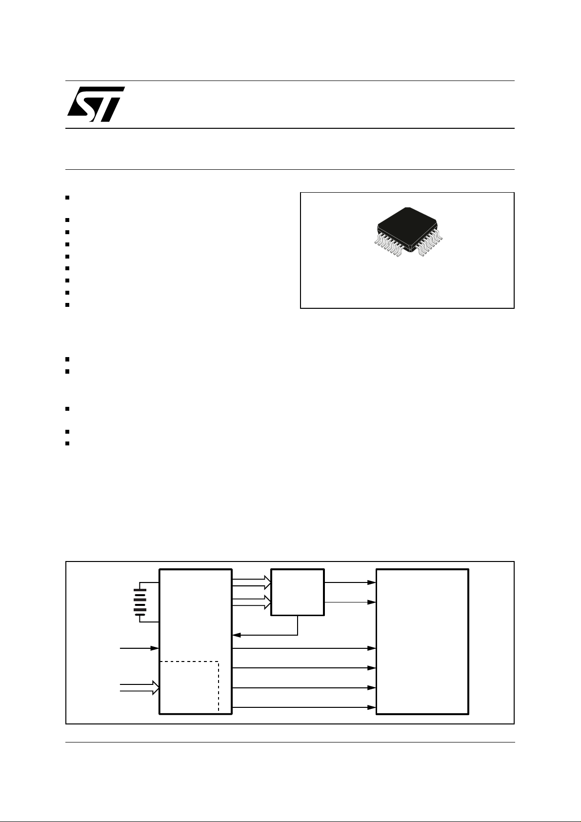
PACKAGE: TQFP32
APPLICATION
NOTEBOOK AND SUBNOTEBOOK COMPUTERS
PEN TOP AND PO RTABLE EQUIPMENT
COMMUNICATING COMPUTE RS
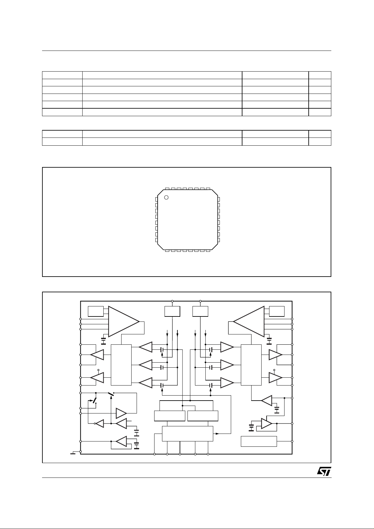
DESCRIPTION
The L4992 is a sophisticated dual PWM stepdown controller and power monitor intended for
Notebook computer and/or battery powered
equipment. The device produces regulated
+3.3V, +5.1V and 12V supplies for use in portable
L4992
TQFP32
ORDERING NUMBER: L4992
and PCMCIA applications.
The internal architecture allows to operate with
minimum external components count. A very high
switching frequency (200/300 KHz or externally
synchronizable) optimizes their physical dimensions.
Synchronous rectification and pulse skipping
mode for the buck sections optimise the overall
efficiency over a wide load current range (96% efficiency @1A/5.1V and 93% efficiency @
0.05A/5.1V.
The two high performance PWM controllers for
+3.3V and +5.1V lines are monitored for overvoltage, undervoltage and overcurrent conditions.
On detection of a fault, a POWER GOOD signal
is generated and a specific shutdown procedure
takes place to prevent physical damage and data
corruption.
A disable function allows to manage the output
power sections separately, optimising the quiescent consumption of the IC in stand-by conditions.
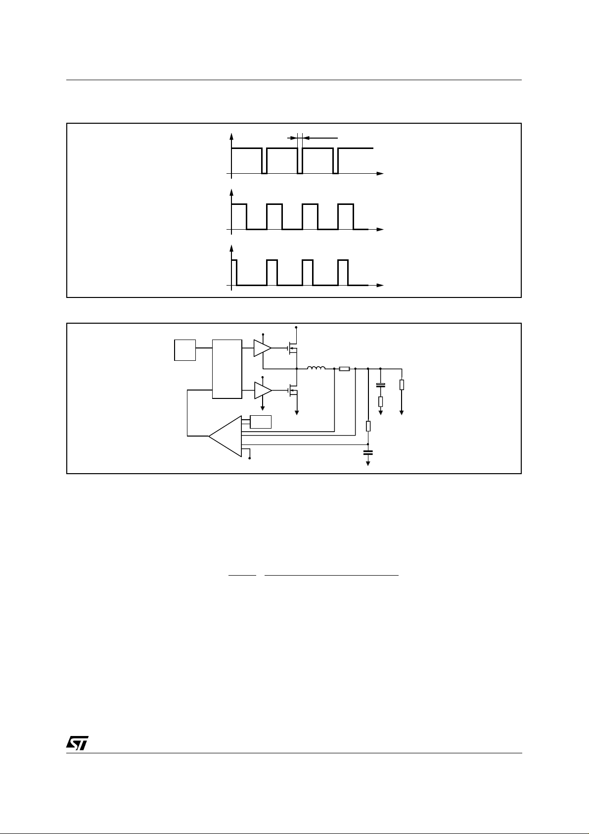
SYSTEM BLOCK DIAGRAM
5.5V
to
25V
SYNC
POWER
MANAGEMENT
& SYSTEM
SUPERVISOR
D96IN429A
June 2000
L4992
POWER
SECTION
3.3V
5.1V
12V LDO
5.1V LDO
3.39V REF
POWER GOOD
µP
MEMORY
PERIPHERALS
1/26
L4992
ABSOLUTE MAXIMUM RATINGS
Symbol Parameter Value Unit
V
IN
V
I
I
IN
I
OUT
T
J
THERMAL DATA
Symbol Parameter Value Unit
R
TH J-amb
Power Supply Voltage on V
IN
0 to 25 V
Maximum Pin Voltage to Pins 1, 24, 25, 32 -0.5 to (VIN +5) V
Input Current Except V13IN and V
IN
-1 to +1 mA
Output Current Digital Output -15 to +15 mA
Junction Temperature -55 to 150 °C
Thermal Resistance Junction -Ambient 60 °C/W
PIN CONNECTION
BLOCK DIAGRAM
6
I5SNS
5
V5SNS
7
COMP5
1
H5STRAP
32
H5GATE
31
H5SRC
30
R5GATE
29
PGND5
REG5
3
4
W5SW
2
VIN
12VREF
SGND
13
(Top view)
H5GATE
R5GATE
H5SRC
PGND5
PGND3
R3GATE
H3SRC
H3GATE
32 3031 29 28 27 26 25
H5STRAP
(*)TO BE CONNECTED TO PIN13
+
SLOPE
VREF
Hside
REG5 REG5
Lside
COMPARATOR
VREF BUFFER
-
+
-
+
-
CONTROL
SWITCH
ERROR SUMMING
∑
LOGIC
LINEAR
REGULATOR
-
+
+
-
OVER CURRENT
COMPARATOR
ZERO CROSSING
COMPARATOR
PULSE SKIPPING
COMPARATOR
V5SNS
VREF
1
2
VIN
3
REG5
4
V5SW
5
V5SNS
6
I5SNS
7
COMP5
8
SOFT5
910
11 12 13 14 15 16
VREF
CRST
RUN5
PWROK
SOFT5
8
SOFT
I5SNS V5SNS
+
-
+
-
+
-
OVERVOLT
COMPARATOR
4.7V
RUN3 RUN5 PWROK NOSKIP CRST
POWER MANAGEMENT
&
SYSTEM SUPERVISOR
16 11 10 14 9
SGND
COMPARATOR
OSC
NOSKIP
SOFT3
17
SOFT
I3SNSV3SNS
UNDERVOLT
24
H3STRAP
23
(*)
22
REG12
21
V13IN
20
V3SNS
19
I3SNS
18
COMP3
17
SOFT3
D96IN377
RUN3
OVER CURRENT
COMPARATOR
+
-
ZERO CROSSING
COMPARATOR
+
-
PULSE SKIPPING
COMPARATOR
+
-
ERROR SUMMING
VREF
+
+
∑
+
-
VREF
CONTROL
LOGIC
13V UV Comp
+
-
OSCILLATOR &
SYNCHRONIZATION
13V
Hside
Lside
+
-
SLOPE
D96IN375
REG12
LDO
19
I3SNS
20
V3SNS
18
COMP3
24
H3STRAP
25
H3GATE
26
H3SRC
27
R3GATE
28
PGND3
21
V13IN
22
REG12
15
OSC
2/26

PIN FUNCTIONS
N. Name Description
1 H5STRAP +5.1V section bootstrap capacitor connection
2V
IN
3 REG5 +5V regulator supply. Used mainly for bootstrap capacitors. It should be bypassed to ground.
4 V5SW Alternative device supply voltage. When the +5.1V section is operating, the device is no
5 V5SNS This pin connects to the (-) input of the +5.1V internal current sense comparator
6 I5SNS This pin connects to the (+) input of the +5.1V internal current sense comparator
7 COMP5 Feedback input for the +5.1V section.
8 SOFT5 Soft-start input of the +5.1V section. The soft-start time is programmed by an external
9 CRST Input used for start-up and shut-down timing. A capacitor defines a time of 2ms/nF.
10 PWROK Power-good diagnostic signal. This output is driven high when both switching sections are
11 RUN5 Control input to enable/disable the 5.1V section. A high level (>2.4V) enables this section, a
12 VREF Internal +3.39V high accuracy voltage generator. It can source 5mA to external load. Bypass
13 SGND Signal ground. Reference for internal logic circuitry. It must be routed separately from high
14 NOSKIP Pulse skipping mode control. A high level (>2.4V) disables pulse skipping at low load current,
15 OSC Oscillator frequency control: connect to 2.5V to select 300KHz operation, to ground or to 5V
16 RUN3 Control input to enable/disable the +3.3V section. A high level (>2.4V) enables this section, a
17 SOFT3 Soft-start input for the 3.3V section. The soft-start time is programmed by an external
18 COMP3 Feedback input for the +3.3V section
19 I3SNS This pin connects to the (+) input of the +3.3V internal current sense comparator
20 V3SNS This pin connects to the (-) input of the +3.3V internal current sense comparator
21 V13IN 12V regulator input supply voltage, included between 13 and 20V. This voltage can be
22 REG12 12V regulator output voltage. It can source up to 150mA to an external load
23 SGND To be connected to pin 13
24 H3STRAP +3.3V section bootstrap capacitor connection
25 H3GATE Gate- driver output for the +3.3V high-side N-MOS
26 H3SRC +3.3V high-side N-MOS source connection
27 R3GATE Gate- driver output for the +3.3V low- side N-MOS (synchronous rectifier).
28 PGND3 Current return for +3.3V section drivers
29 PGND5 Current return for +5.1V section drivers
30 R5GATE Gate-driver output for the +5.1V low-side N-MOS (synchronous rectifier).
31 H5SRC +5.1V high-side N-MOS source connection
32 H5GATE Gate-driver output for the +5.1V high-side N-MOS
Device supply voltage. From 5.5 to 25V
longer powered through V
but through this pin.
IN
capacitor connected between this pin and SGND. Approximately, 1ms/nF @ full load.
enabled and running properly, after a delay defined by the CRST capacitor.
low level (<0.8V) shuts it down
to ground with a 4.7µF capacitor to reduce noise.
current returns.
a low level (<0.8V) enables it.
for 200KHz operation. A proper external signal can synchronize the oscillator
low level (>0.8V) shuts it down.
capacitor connected between this pin and GND. Approximately, 1ms/nF @full load.
supplied by a flyback winding on +3.3V inductor
L4992
3/26
L4992
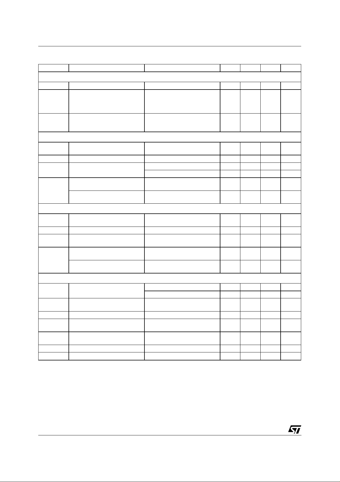
ELECTRICAL CHARACTERISTICS
IN
= 12V; TJ = 25°C; V
(V
OSC
= GND; unless otherwise specified.)
Symbol Parameter Test Condition Min. Typ. Max. Unit
DC CHARACTERISTICS
V
IN
I
2
I
2
+5.1V PWM CONTROLLER SECTION
V
5OUT
- V
V
6
V6 - V
V
5
Input Supply Voltage 5.5 25 V
Operating Quiescent Current R5GATE = R3GATE = OPEN
H5GATE = H3GATE = OPEN
RUN3 = RUN5 = REG5
(DRIVERS OFF)
Stand-By Current RUN3 = RUN5 = GND
V
V
= 12V
IN
= 20V
IN
50
60
(*) V5SNS Feedback Voltage VIN = 5.5 to 20V;
V
- V
I5SNS
Over-Current Threshold Voltage VSOFT5 = 4V 80 100 120 mV
5
Pulse Skipping Mode
5
Thereshold Voltage
VIN > 6.8V 14 26 38 mV
< 5.8V 7 13 19 mV
V
IN
= 0 to 70mV
V5SNS
Over Voltage Threshold ON
V5SNS
Under Voltage Threshold ON
V5SNS
4.85 5.13 5.25 V
5.35 5.55 5.77 V
4.54 4.69 4.87 V
1.35 mA
100
120
+3.3V PWM CONTROLLER SECTION
V
(*) V3SNS Feedback Voltage VIN = 5.5 to 20V;
3OUT
V19 - V
- V
V
19
Over Current Threshold Voltage VSOFT3 = 4V 80 100 120 mV
20
Pulse Skipping Mode Threshold
20
V
I3SNS
VIN = 5.5 to 20V; 14 26 38 mV
Voltage
V
20
Over Voltage Threshold ON
V3SNS
Under Voltage Threshold ON
V3SNS
- V
= 0 to 70mV
V3SNS
3.285 3.39 3.495 V
3.55 3.7 3.85 V
3.02 3.14 3.27 V
µA
PWM CONTROLLERS CHARACTERISTICS (BOTH SECTIONS)
F
OSC
V
15
T
OFF
T
OV
T
UV
, I
I
8
, V
V
8
(*) Guaranteed by design, not tested in production
4/26
Switching Frequency Accuracy OSC = REG5/2 255 300 345 kHz
OSC = 0 or REG5 170 200 230 kHz
Voltage Range for 300kHz
Operation
Dead Time 300 375 450 ns
Overvoltage Propagation Time V5SNS to PWROK or
V3SNS to PWROK
Undervoltage Propagation Time V5SNS to PWROK or
V3SNS to PWROK
Soft Start Charge Current 3.2 4 4.8 µA
17
Soft Start Clamp Voltage 4 V
17
2.4 2.6 V
1.25 µs
1.5 µs
L4992
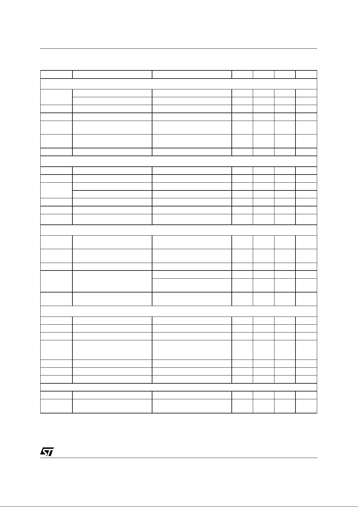
ELECTRICAL CHARACTERISTICS
(Continued)
Symbol Parameter Test Condition Min. Typ. Max. Unit
HIGH AND LOW SIDE GATE DRIVER (BOTH SECTIONS)
I25, I
I32, I
R
R
V
V
T
H
L
OH
OL
CC
Source Output Peak Current C
27,
30
Sink Output Peak Current C
R
Resistance (or Impeda nce ) Driver OUT HIGH 7 Ω
DSON
R
resistance (or Impedance) Driver OUT LOW 5 Ω
DSON
Output High Voltage HSTRAP = REG5
= 1nF 0.2 0.5 A
LOAD
= 1nF 0.2 0.5 A
LOAD
4.40 5.3 5.61 V
I
= 10mA; HSRC = GND
SOURCE
Output Low Voltage HSTRAP = REG5
I
= 10mA HSRC = GND
SINK
Cross-Conduction Delay 30 75 130 ns
0.5 V
12V LINEAR REGULATOR SECTION
V
21
V
22
I
22
V
CP
Input Voltage Range 13 20 V
Output Voltage I22 = 0 to 120mA 11.54 12.0 12.48 V
Current Limiting V
Short Circuit Current V
Input Voltage Clamp I
"One Shot" Activation Threshold V
= 12V 120 mA
REG12
= 0V 150 mA
REG12
= 100µA16 V
CLAMP
Falling 12.88 13.7 14.52 V
13IN
"One Shot" Pulse 1.5 µs
INTERNAL REGULATOR (VREG 5) AND REFERENCE VOLTAGE
V
3
I
3
V
12
I
12
VREG5 Output Voltage VIN = 5.5 to 20V
I
= 0 to 5mA
LOAD
Total Current Capability VREG5 = 5.3V
V
= 6V
REG5
4.5 5.3 5.61 V
25
70
Switch-Over Threshold Voltage 4.3 4.53 4.7 V
Reference Voltage 3.35 3.39 3.43 V
Source Current at Reference
= 5.5 to 20V
V
IN
I
= 1 to 5mA
LOAD
3.32 3.39 3.46 V
5mA
Voltage
mA
POWER GOOD AND ENABLE FUNCTION
V16, V
, V
V
16
T
10
, T
T
27
SYNCHRONIZATION
RUN3, RUN5, Enable Voltage HIGH LEVEL 2.4 V
11
RUN3, RUN5, Disable Voltage LOW LEVEL 0.8 V
11
Power Good Delay C
Shutdown Delay Time before
30
Low Side Activation
(Except Over-Voltage Fault)
CRST Timing Rate 2 ms/nF
Power Good High Level I
Power Good LowLevel I
Synchronisation Pulse Width 400 ns
Synchronisation Input Voltage
(Falling Edge Transition)
= 100nF 160 200 240 ms
CRST
C
= 100nF, 160 200 240 ms
CRST
= 40µA 4.1 V
PWROK
= 320µA 0.4 V
PWROK
5V
5/26

L4992
DETAILED FUNCTIONAL DESCRIPTION
In the L4992 block diagram six fundamental functional blocks can be identified:
3.3V step-down PWM switching regulator (pins 17 to 20, 24 to 27).
5.1V step-down PWM switching regulator (pins 1, 4 to 8, 30 to 32).
12V low drop-out linear regulator (pins 21,22).
5V low drop-out linear regulator (pin 3).
3.3V reference voltage generator (pin 12).
Power Management section (pins 9 to 11, 14,16).
The chip is supplied through pin VIN (2), typically by a battery pack or the output of an AC-DC adapter,
with a voltage that can range from 5.5 to 25V. The return of the bias current of the device is the signal
ground pin SGND (13), which references the internal logic circuitry.
The drivers of the external M OSFET’s have their separate current return for each section, namely the
power ground pins PGND3 (28) and PGND5 (29). Take care of keeping separate the routes of signal
ground and the two power ground pins when laying out the PCB (see "Layout and grounding" section).
The two PWM regulators shar e the internal oscillator, pr ogr ammable or s yn chronizable through pin OSC
(15).
+3.3V AND +5.1V PWM REGULATORS
Each PWM regulator includes control circuitry as well as gate-drive circuits for a step-down DC-DC con-
verter in buck topology using synchronous rectification and current mode control.
The two regulators are independent and almost identical. As one can see in the Block Diagram, they
share only the oscillator and the internal supply and differ f or the pre- set output v oltages and f or t he c ontrol circuit that links the +3.3V section to the operation of the 12V linear regulator (see the relevant section).
Each converter can be turned on and off independently: RUN3 and RUN5 are control inputs which disable the relevant section when a low logic level (below 0.8 V) is applied and enable its operation with a
high logic level (above 2.4 V). When both input s are low the device is in stand- by condition and its current consumption is extremely reduced (less than 120µA over the entire input voltage range).
Oscillator
The oscillator, which does not require any external timing component, controls the PWM switching frequency. This can be either 200 or 300 kHz, depending on the logic s tate of the control pin OSC, or else
can be synchronized by an external oscillator.
If OSC is grounded or connected to pin REG5 (5V) the oscillator works at 200kHz. By connecting OSC to
a 2.5 V voltage, 300 kHz operation will be selected. I nstead, if pin OSC is fed with an ex ternal signal like
the one shown in fig. 1, the oscillator will be synchronized by its falling edges.
Considering the spread of the oscillator, synchronization can be guaranteed for frequencies above
230kHz. Even though a maximum frequency value is in pr actice imposed by efficiency considerations it
should be noticed t hat increasing frequency too much arises problem s (noise, subharmonic oscillation,
etc.) without significant benefits in terms of external component size reduction and better dynamic performance.
The oscillator imposes a time interval (300 ns min.), during which the high-side MOSFET is definitely
OFF, to recharge the bootstrap capacitor ( see "MOSFET’s Drivers" section). This, implies a limit on the
maximum duty cycle (88.5% @ fsw = 300kHz, 92.6% @ fsw = 200kHz, worst case) which, in turn, imposes a limit on the minimum operating input voltage.
PWM regulati on
The control loop does not employ a tradit ional error amplifier in favour of an error summing comparator
which sums the reference voltage, the feedback signal, the voltage drop across an external sense resistor and a slope compensation ramp (to avoid subharmonic oscillation with duty cycles greater then 50%)
with the appropriate signs.
The output latch of both controllers is set by every pulse coming from the oscillator. That turns off the
low-side MOSFET (synchronous rectifier) and, after a short delay (typ. 75 ns) to prevent cross-conduction, turns on the high-side one, thus allowing energy to be drawn from the input source and stored in the
inductor.
6/26
L4992
DETAILED FUNCTIONAL DESCRIPTION
Figure 1:
Figure 2:
Synchronization signal and operation.
OSC
5V
0V
H5GATE
H3GATE
L4992 Control Loop.
CLOCK
SRQ
E.S.
_
Q
+
+
-
+
(continued)
HSTRAP
REG5
SLOPE
COMP.
VREF
400ns min.
VIN
L
D97IN574
Rsense
t
t
t
Co
Ro
ESR
Rf
Cf
The error summing, by comparing the above mentioned signals, determines the moment in which the
output latch is to be reset. The high-side MOSFET is then turned off and the synchronous rectifier is
turned on after the appropriate delay (typ. 75 ns), thus making the inductor current recirculate. This state
is maintained until the next oscillator pulse.
With reference to the schematic of fig. 2, the open-loop transfer function of such a kind of control system,
under the assumption of an ideal slope compensation, is:
F(s) = A⋅
R
R
O
sense
⋅
(1 +
1 + s ⋅ ESR ⋅ C
s ⋅ R
O CO
) ⋅ (1 +
O
s ⋅ R
F CF
)
where A is the gain of the error summing comparator, which is 2 by design.
The system is inherently very fast since it tends to correct output voltage deviations nearly on a cycle-by-
cycle basis. Actually, in case of line or load changes, few switching cycles can be sufficient for the transient to expire.
The operation above illustrated is modified during particular or anomalous conditions. Leaving out other
circumstances (described in "Protections" section) for the moment, consider when the load current is low
enough or during the first switching cycles at start-up: the inductor current may become discontinuous,
that is it is zero during the last part of each cycle. In such a case, a "zero current comparator" detects the
event and turns off the synchronous rectifier, avoiding inductor current reversal and reproducing the
natural turn-off of a diode when reverse biased. Both MOSFET’s stay in off state until the next oscillator
pulse.
7/26
L4992
DETAILED FUNCTIONAL DESCRIPTION
(continued)
Synchronous rectification.
Very high efficiency is achieved at high load current with the synchronous rectification technique, which
is particularly advantageous because of the low output voltage. The low-side MOSFET, that is the synchronous rectifier, is selected with a very low on -resistance, so that the paralleled Schottky diode is not
turned on, except for the small time in which neither MOSFET is conducting. The effect is a considerable
reduction of power loss during the recirculation period.
Although the Schottky might appear to be redundant, it is not in a system where a very high efficiency is
required. In fact, it s lower threshold prevent s the lossy body-diode of the synchronous rectifier MOSFET
from turning on during the above mentioned dead-time. Both conduction and reverse recovery losses are
cut down and efficiency can improve of 1-2% in some cases. Besides a small diode is sufficient since it
conducts for a very short time.
As for the 3.3V section only, the synchronous rectifier is also involved in the 12 V linear regulator operation (see the relevant section). See also the "Power Management" to see how both synchronous rectifiers are used to ensure zero voltage output in stand-by conditions or in case of overvoltage.
Pulse-skippi ng operation.
To achieve high efficiency at light load current as well, under this condition the regulators change their
operation (unless this feature is disabled): they abandon PWM and enter the so-called pulse-skipping
mode, in which a single switching cycle takes place every many oscillator periods.
The "light load condition" is det ected when the v oltage across the external sense resistor (V
Rsense
) does
not exceed 26mV while the high-side MOSFET is conducting. When the reset s ignal of the output latch
comes from the error summing comparator while V
reset is driven as soon as V
reaches 26mV. This gives some extra energy that maintains the output
Rsense
is below this value, it is ignored and the actual
Rsense
voltage above its nominal value for a while. The oscillator pulses now set the output latch only when the
feedback signal indicates that the output voltage has fallen below its nominal value. In this way, most of
oscillator pulses is skipped and the r esulting s witching frequency is much lower, as expressed by the following relationship:
2
R
K ⋅
sense
L
⋅ I
where K = 3.2 ⋅ 10
=
f
ps
3
and fps is in Hz. As a result,
the losses due to switching and to gate-drive,
⋅ V
out
Figure 3:
out
⋅
1
V
out
−
V
in
Pulse-skipping threshold vs. input
voltage (+5.1V section only).
which mostly account for power dissipat ion at low
output power, are considerably reduced.
The +5.1V section can work with the input voltage
very close to the output one, where the current
waveform may be so flat to prevent pulse-skipping
from being activated. To avoid this, the pulse-skip-
Vth
26 mV
ping threshold (of the +5.1V section only) is
roughly halved at low input voltages, as shown in
fig. 3. Under this condition, in the above formula
the constant K becomes 12.8 ⋅ 10
3
.
13 mV
When in pulse-skipping, the output voltage is
some ten mV higher than in PWM mode, just be-
5.5V 5.8V 6.3V 20V
Vin
cause of its mode of operation. If this "load regulation" effect is undesirable for any reason, the pulse
skipping feature can be disabled (see "Power
Management" section) to the detriment of efficiency at light load.
MOSFET’s drivers
To get the gate-drive voltage for the high-side N-channel MOSFET a bootstrap technique is employed. A
capacitor is alternately charged through a diode from the 5V REG5 line when the high-side MOSFET is
OFF and then connected to its gate-source leads by the internal floating driver to turn the MOSFET on.
The REG5 line is used to drive the synchronous rectifier as well, and therefore the use of low-threshold
8/26

L4992
DETAILED FUNCTIONAL DESCRIPTION
(continued)
MOSFET’s (the so-called "logic-level" devices) is highly recommended.
The drivers are of "dynamic" type, which means they do not give origin to current consumption when
they are in static conditions (ON or OFF), but only during transitions. This featur e is aimed at minimizing
the power consumption of the device even during stand-by when both low-side MOSFET’s are ON.
Protections
Each converter is fully protected against fault conditions. A monitoring system checks for overvoltages of
the output, quickly disabling both c onverters in case such an event occurs. This condition is latched and
to allow the device to start again either the supply voltage has to be removed or both RUN3 and RUN5
pins have to be driven low.
Undervol tage condit ions are de tected as wel l but do n ot cau se int errupt ion of t he op erat ion of the conve rters. O n ly PWROK si gnal (a t p in 10) reveal s t h e anoma ly with a low outp ut level .
If the chip overheats (above 135 °C typ.) the device stops operating as long as the temperature falls below a
safe value (105 °C typ.). The overtemperature condition is signalled by a low level on PWROK as well.
A current limitation comparator prevents f rom excessive current in case of overload or short-circuit. It intervenes as the voltage VRsense exceeds 100 mV, turning off the high-side switch before the error summing does. By the way, this also gives the designer the ability to program the maximum operating current
by selecting an appropriate sense resistor.
This pulse-by-pulse limitation gives a quasi-constant current characteristic. If a "folded back" characteristic, like the one shown in Fig. 4a, is desired the external circuit of Fig. 4b can be used. The circuits
acts on the current limitation and is extremely simple and cheap. The advantage of such a technique i
that a short circuit will cause a current much lower than the maximum to flow. Th e stress of the power
components will be very litt le and no overheating will occur. The part values shown in Fig. 4b produce
IFOLD = 1A in the Demo Board (see the relevant section).
Inrush current at start-up is reduced with soft-start. An external capacitor (one for each converter) is
charged by an internal 4µA current generator and its linearly ramping volta ge increases the setpoint of
the current limit comparator, starting from zero up t o the f inal value of 100 mV. Thus duty cycle reaches
gradually its steady-state value and dangerous current peaks as well as overshoots of the out put voltage
are avoided.
+12 V LINEAR REGULATOR
The +12V Linear regulator is capable of delivering up to 120 mA to an external load through pin REG12.
It is supplied from pin V13IN which accepts voltages included in the range of 13 to 20V.
If the application works with input volt ages included between 14 and 20V, the supply for the regulator
can be obtained directly from the input source. If such is not the case, the most convenient way to get
the supply is to use an auxiliary winding on the 3.3 V section inductor with a catch diode, Ds, and a filter
capacitor, Cs, as shown in fig. 5. This winding delivers energy t o pin V13IN during the r ecirculation period of each switching cycle with a voltage determined by the turns ratio n and little dependent on the input voltage.
Figure 4.
V
IN
V
REF-VF
V
-0.1
O
I
FOLDImax
(a)
32(25)
31(26)
30(27)
L4992
I
O
6(19)
5(20)
1N4148
12
L
6.8KΩ
(3.9KΩ)
(b)
R
sense
100Ω
5V(3.3V)
D98IN815
C
O
9/26

L4992
DETAILED FUNCTIONAL DESCRIPTION
(continued)
An auxiliary winding could be used also on the choke of the +5.1V section, either to power the +12V linear regulator or to derive a further supplemental output, however the 3. 3 V section has been provided
with some features aimed at ensuring a proper operation under all circumstances.
For a correct operation of the regulator, the voltage at pin V13IN must not be too low. The flyback connection of the two windings ensures a well regu lated voltage, provided t here is good m agnetic coupling.
The coupled inductors configuration, however, is not able to sustain the auxiliary voltage if the main output is lightly loaded: the secondary voltage drops and the system goes out of regulation.
To overcome this problem, when the V13IN voltage f alls below a certain threshold (13.7 V +/- 5%) because of too light a load on the 3.3V section, the relevant synchronous rectifier is turned on for 1.5 µs
max. during the interval in which the inductor current is zero ("one-shot" feature, see fig. 6). In this way,
the inductor current reverses and draws from the output capacitor energy which is forward transferred to
the auxiliary output.
In case the 3.3V section is wor king at f ull load and the linear regulator is lightly loaded, the voltage at pin
V13IN can exceed the expected value. In fact, Ds and Cs act as a peak-holding circuit and V13IN is influenced by the voltage spikes at switching transients. An internal clamp limits the voltage but, in case of
intervention, the chip power dissipation will rise.
When the 3.3V regulator is disabled, the linear regulator is disabled as well and is plac ed in a low-power
mode to reduce device consumption.
Figure 5:
12V regulator supply with auxiliary winding.
D
S
n
1
3.3V
to V13IN
C
S
Figure 6:
"One shot" feature to sustain V13IN voltage.
H3GATE
1.5µs
L3GATE
IL
V13IN
13.7V
D97IN575
D97IN576A
t
t
t
t
10/26

L4992
DETAILED FUNCTIONAL DESCRIPTION
(continued)
+5 V LINEAR REGULATOR & +3.3 V REFERENCE VOLTAGE GENE RATOR
This low drop-out regulator power s almost all the internal circuitry, that is the +3.3V reference voltage
generator, amplifiers, comparators, digital logic, and MOSFET drivers. Its output is externally available
through pin REG5.
The typical external use of this generator is to c harge the boot strap capacitors used to produce the gatedrive voltage for the high-side MOSFET’s of both PWM converters.
At start-up and when the 5V section is not operating, this regulator is powered by the chip input voltage.
To reduce power consumption, the linear regulator is turned off and the REG5 pin is internally connected
to the 5V PWM regulator output via V5SW pin, when the 5V PWM regulator is active and its output voltage is above the switchover threshold, 4.5V.
The 5V regulator is always active, even if both PWM regulators are disabled, as long as power is applied
to the chip.
The 3.3V reference voltage generator, which is active only when either PWM converter is enabled, provides comparison levels for threshold detection and device operat ion. It is allowed to source up to 5mA
to an external load from its buffered output, externally available through pin VREF.
If either REG5 or VREF does not deliver the correct voltage, the device is shut down.
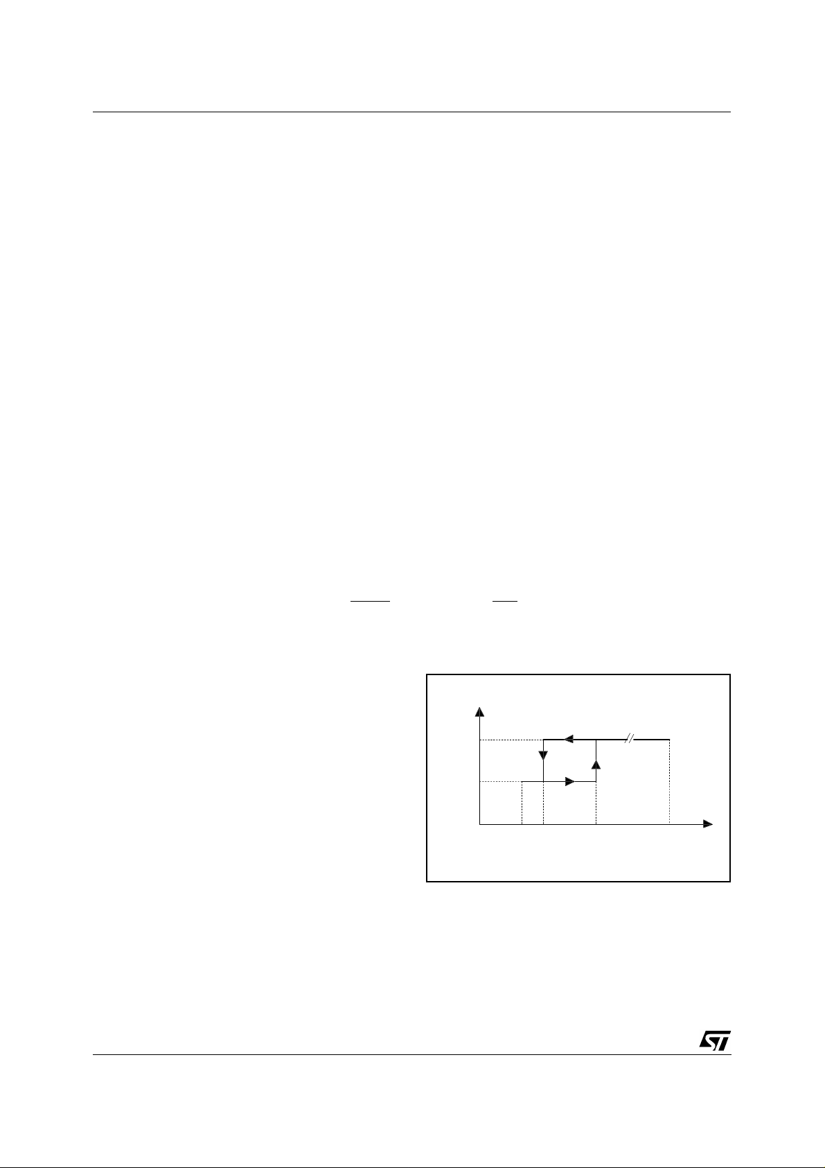
POWER MANAGEMENT
The L4992 is provided with some control pins suitable to perform some functions which are commonly
used or sometimes required in bat tery-operated equipment. Besides, it features controlled timing sequences in case of turn-on/ off and device shutdown for a safe and reliable behaviour under all conditions.
As above mentioned, RUN3 and RUN5 pins allow to disable separately both PWM converters by means
of logic signals (likely coming from a µP) as mentioned earlier.
NOSKIP can disable the pulse-skipping feature: when it is held high neither of the PWM regulators is allowed to enter this kind of operation.
The PWROK output signal drives low immediately when either PWM regulator output falls below its own
undervoltage threshold or when either of them is disabled. It is high when both regulator run properly.
A capacitor connected between CRST and ground fixes a time, in the order of 2ms/nF, which delays the
transition low-high of PWROK. This happens at start-up or after recovering an undervoltage condition,
provided both RUN3 and RUN5 are high. The delay starts from the moment in which the output voltage
has reached its correct value for both sections.
The same delay intervenes also in another circumstance: when a section is disabled (because its RUN is
driven low or owing to a thermal shutdown), the relevant synchronous rectifier is turned on after the
above delay in order to make sure that the load is no longer supplied.
This delay, however, does not intervene in case of overvoltage: the synchronous rectifier is immediately
turned on after the shutdown, thus acting as a built-in "crowbar".
All these timing sequences are illustrated in Fig 7.
11/26

L4992
DETAILED FUNCTIONAL DESCRIPTION
Figure 7:
L4992 controlled timing sequences.
RUN3
VOUT3
RUN5
VOUT5
CRST
PWROK
a) TURN-ON TIMING SEQUENCE
(continued)
t
t
t
t
t
t
RUN3
t
VOUT3
t
H3GATE
t
R3GATE
t
CRST
t
PWROK
t
RUN5
t
VOUT5
t
H5GATE
t
RUN3
VOUT3
H3GATE
R3GATE
CRST
PWROK
RUN5
VOUT5
H5GATE
R5GATE
c) SHUTDOWN TIMING SEQUENCE (2)
R5GATE
t
t
VOUT3
t
H3GATE
t
R3GATE
t
CRST
t
PWROK
t
VOUT5
t
H5GATE
t
R5GATE
t
b) SHUTDOWN TIMING SEQUENCE (1)
d) OVP TIMING SEQUENCE
D97IN577
t
t
t
t
t
t
t
t
12/26

L4992
DESIGN PROCEDURE
Basically, the application circuit topology is fixed, and the design procedure concerns only the selection
of the component values suitable for the voltage and current requirements of the specific application.
The design data one needs to know are therefore:
Input voltage range: the minimum (V
tion is expected to operate;
Maximum load current for each of the three sections:
- I
for the +3.3V section;
out3
- I
for the +5.1V section:
out5
- I
for the +12V section;
out12
Maximum peak-to-peak ripple amplitude of the output voltage for each switching section:
for the +3.3V section;
- V
rpp3
- V
for the +5.1V section;
rpp5
The operating frequency fsw (200/300 kHz or externally synchronized).
It is worth doing some preliminary con siderations. The selection of the switching frequency depends on
the requirements of the application. If the aim is to minimize the size of the external components, 300
kHz will be chosen. For low input voltage applications 200 kHz is preferred, since it leads to a higher
maximum duty cycle.
As for the switching regulators, the inductance value of the output filter affects the inductor current ripple:
the higher the inductance the lower the ripple. This implies a lower current sense resistor value (for a
given I
), lower core losses and a lower output voltage ripple (for a given output capacitor) but, on the
out
other hand, more copper losses and a worse transient behaviour due t o load ch anges. Usually the maximum ripple peak-to-peak amplitude (which occurs at V
load current. It is convenient to introduce a ripple factor coefficient, RF, that is therefore a number between 0.15 and 0.5.
As for the linear regulator, its input voltage V
winding should be dimensioned to get this voltage with a certain margin (say, 14V). Conversely, an
higher input voltage leads to higher losses inside the regulator, to the detriment of efficiency, and to
higher total current on the +3.3V inductor. Besides it implies a higher turns ratio and therefore a worse
magnetic coupling, which affect energy transfer during flyback.
) and the maximum (V
inmin
inmax
should not fall below 13V and therefore the auxiliary
inlin
) voltage under which the applica-
inmax
) is chosen between 15% and 50% of the full
SWITCHING REGULATORS
+5.1V Induct or
To define the inductor, it is necessary to determine firstly the inductance value. Its minimum value is
given by:
and a value L5 > L5
should be selected.
min
L
5min
=
5.1
V
in max
(
⋅
V
max
in
f
⋅
⋅
sw
− 5.1
I
out5
)
⋅ RF
Core geometry selection is connected to the requirements of the specific application in terms of space
utilization and other practical issues like ease of mounting, availability and so on. As to the material, the
choice should be directed towards ferrite, molypermalloy or Kool M
®
µ
, to achieve high efficiency. These
materials provide low core losses (ferrite in particular), so t hat the design can be concentrated on preventing saturation and limiting copper losses.
Saturation must be avoided even at maximum peak current:
I
L5pk
= I
out5
+
5.1
2
⋅
V
in max
⋅
⋅
f
L5 ⋅ V
sw
− 5.1
in max
)
(
To limit copper losses, the winding DC resistance, RL, should be as low as possible (in the range of mΩ).
AC losses can usually be neglected. A practical criterion to minimize DC resistance could be to use the
largest wire that fits the selected core.
Anyway the best solution, whenever possible, is to use an off-the-shelf inductor whic h meets the requir ements in terms of inductance and maximum DC current. Nowadays there is a broad range of products
13/26

L4992
DESIGN PROCEDURE
(continued)
offered by manufacturer, also for surface mount assemblies.
+3.3 V Transformer
The primary winding carries the secondary power as well, thus the total primary average current is:
V
⋅ I
inlin
I
= I
out3
+
where V
tot3
is the voltage generat ed during the recirculation of the primary and fed into t he input of the
inlin
+12V linear regulator. The turns ratio 1:n of the transformer is chosen so that V
3.3
out12
is above 13V. To re-
inlin
duce the turns ratio in order to minimize stray parameters, the secondary is referred to the 3.3V output,
and therefore the minimum value is given by:
V
− 3.3 + V
min
3.3
inlin
=
n
f
where Vf is the forward drop ac ross the rectifier ( assume 1V to be conservative). Make sure the secondary is connected with the proper polarity (see fig. 6).
The minimum primary inductance value can be expressed as:
2
−
)
⋅ I
out12
− 3.3
in
3.3
in
−
3.3) − n
in
⋅
Vin ⋅ I
out12
]
)
3
⋅
=
4
L
3pmin
where RF, to get positive values for L
3.3 ⋅ (V
Vin ⋅ fsw ⋅ [I
, must satisfy the inequality:
3pmin
RF
⋅ RF ⋅ (V
tot3
n
>
I
tot3
⋅
V
in
(
⋅
V
and where Vin can be either V
With a primary inductance L
inmin
3p
> L
or V
3pmin
, whichever gives the higher value for L
inmax
3pmin
.
the primary peak current, whic h must not saturat e the magnetic
core, will be:
−
)
I
L3pk
=
I
tot3
+
2 ⋅
3.3 ⋅ (V
f
sw
⋅
in max
L
3p
3.3
+ n ⋅ I
⋅
V
in max
out12
As to the transformer realization, the considerations regarding to the +5.1V inductor can be here repeated.
Power MOSFET’s and Schottky diodes
Since the gate drivers of the L4992 are powered by a 5V bus , the use of logic-level MOSFET’s is highly
recommended, especially for high current applications. Their breakdown voltage V
greater than V
The R
DS(ON)
with a certain margin, so the selection will address 20V or 30V devices.
inmax
can be selected once the allowable power dissipation has been established. By selecting
(BR)DSS
must be
identical power MOSFET’s as the main switch and the synchronous rectifie r, the total power t hey dissipate does not depend on the duty cycle. Thus, if P
power), the required R
where I
cient of R
is either I
out
DS(ON)
tot3
(typically, α = 5
(@ 25 °C) can be derived from:
DS(ON)
DS(ON
)
or I
R
, according to the section under consideration, α is the temperature coeffi-
out5
-3
⋅
10
°C-1 for these low-voltage classes) and ∆T the admitted tempera-
is this power loss (few percent of the rated output
ON
P
2
⋅ (1 + α
out
ON
⋅
∆T)
=
I
ture rise.
It is worth noticing, however, that generally the lower R
leads to a higher gate drive consumption. In fact, each switching cycle, a charge Q
, the higher is the gate charge Qg, which
DS(ON)
moves from the in-
g
put source to ground, resulting in an equivalent drive current:
⋅
I
= Q
g
f
sw
g
14/26

L4992
DESIGN PROCEDURE
(continued)
which affects efficiency at low load currents. Besides, this current is drawn from the REG5 line whose
source capability, I
FET total gate charge (@ Vgs = 5V);
assuming four identical MOSFET’s.
(25mA min), must not be exceeded, thus a further constraint concernes the MOS-
SRC
I
SRC
≤
Q
g
,
⋅
f
4
SW
The Schottky diode to be placed in parallel to the synchronous rectifier must have a reverse voltage
VRRM greater than Vinmax. Since it conducts for less than 5% of t he switching period, the cur rent r ating
can be much lower than Iout. The selection criterion should be:
V
(schottky) < Vf(body-diode) @ I = I
f
Lpk
Sense Resistors
The sense resistor of each section is selected according to their respective maximum output current. The
current sense comparator limits the inductor peak current and therefore the maximum DC output current
is the peak value less half of the peak-to-peak ripple. The intervention threshold is set at 100 mV for both
sections, thus the resistor values should be:
R
sense5
R
sense3
=
=
100
I
L5pk
100
I
L3pk
[m
[m
Ω]
Ω]
Since the comparator threshold that triggers pulse-skipping mode is 26mV, the output current at which
the system enters this kind of operation is approximately one fourth of the maximum output current.
The sense resistors values are in the low milliohms thus it is important to take correctly the current sense
signals. Make sure that the Kelvin connections between the current sense pins of the IC and the sense
resistor do not carry the output current.
Input Capacitors
A pulsed current (with zero average value) flows through the input capacitor of a buck converter. The AC
component of this current is quite high and dissipates a considerable amount of power on the ESR of the
capacitor:
P
Cin
= ESR
V
⋅ (Vin − V
out
2
⋅
⋅
I
out
2
V
in
out
)
It is easy to find that PCin has a maximum equal to (1/2) ⋅ Iout (@ Vin=2 ⋅ Vout, that is, 50% duty cycle).
The input capacitor of each section, therefore, should be selected for a RMS ripple current rating as high
as half the respective maximum output current.
The capacitance value is not very important but in reality a minimum value must be ensured for stability
reasons. In fact, switching regulators exhibit a negative input impedance that, at low frequencies, is:
2
V
in
−
=
Z
)
in(DC
thus, if the impedance of the power source is not well below the absolute value of Z
V
⋅ I
out
out
at frequencies
in(DC)
up to the bandwidth of the regulator control loop, there is the possibility for oscillations. To ensure stability, the following condition must be satisfied:
L
C
in
>>⋅
ESRin ⋅ | Z
eq
in
(DC)
|
where Leq is the inductance of the circuit upstream the s witching regulator input and ESRin is related to
the input capacitor itself.
The use of high performance electrolytic capacitors is recommended. If a higher cost is of no concern,
OS-CON capacitors are an excellent choice because they offer the smallest size for a given ESR or current rating. Tantalum capacitors do not tolerate pulsed current, so their use is not advisable.
15/26

L4992
DESIGN PROCEDURE
(continued)
Output Capacitors
The output capacitor selection is based on the output voltage ripple requirements. This ripple is related to the
curren t r ippl e t hr ough th e ind uct or an d is alm ost e nt ire ly due t o the ESR of t he ou tp ut cap aci tor . Th ere fore,
the goal is to achieve an ESR lower than a certain value, regardless of the actual capacitance value.
The maximum current ripple of the +5.1V section is:
∆
= 2 ⋅ (I
I
L5
L5pk
- I
out5
)
considering the values obtained in the paragraph "+5.1 V Inductor".
As for the +3.3V, the maximum ripple is given by:
∆
I
= n ⋅ I
L3
where VIN is V
inmin
or V
, as selected in the "+3.3V transformer" section.
inmax
Anyhow, the maximum ESR will be:
out12
⋅
Vin − 3.3
ESR
⋅ (
V
+
∆
rppx
I
Lx
3
4
3.3
⋅
fsw ⋅ L3p ⋅ V
V
V
in
≤
x
)
−
3.3
in
in
where the subscript x refers to either section.
In pulse-skipping operation, the capacitive component of the output ripple is comparable to the resistive
one, thus both should be considered:
(R)
V
= 0.025
rppx
L
(C)
V
rppx
= 3.1
⋅
10
x
−
6
⋅
⋅
C
outx
If specification on the output ripple under pulse-skipping condition is also given, C
2
R
sensex
ESR
X
⋅
R
sense
x
1
⋅
V
in min
1
−
V
out
1
−
V
out
and ESRX must
outx
comply with it as well.
Further constraints on the minimum output capacitance can arise from specifications regarding the maxi-
mum undershoot, ∆V
-
, or overshoot, ∆V
out
C
>
out
∆
V
−
out
⋅ (V
+
, due to a step-load change ∆I
out
2
∆
⋅
I
L
in min
out
⋅
D
max
; C
V
−
out
out
)
>
∆
L ⋅ ∆I
+
V
out
:
out
2
out
V
⋅
out
whichever is greater, and where D
is the maximum duty cycle and the quantities are relevant either to
max
the +3.3V or +5.1V section.
High performance capacitors should be employed to reduce the capacitance needed for a given ESR, to
avoid paralleling several parts with a considerable waste of space. Although ex cellent elec trolytic capacitors are available, OS-CON or tantalums may be preferred especially if very compact design is required,
or in case of surf ace mount assemblies. Multilayer ceramic capacitors with extremely low ESR are now
available, but they have a large spread of the capacitance value, so they should be paralleled with another more stable, high-ESR capacitor.
Miscellaneous components
The feedback loop has virtually un limited bandwidth, thus a filter is necessary to make the system insensitive to the switching frequency ripple and, in gener al, to prevent noise from disturbing the correct operation of the error summing comparator. Anyway, the cut-off frequency of this filter can be very high, so
that line and load transient response is extremely fast. This filter is a simple R-C type where resistance
and capacitance can be chosen for a typical 3dB cut-off frequency of 60 kHz.
As to the bootstrap diodes, even though small signal p-n diodes might be effectively used, it is preferable
to employ low-power Schottky rectifiers, since that increase slightly the gate drive voltage, in favour of efficiency. The bootstrap capacitor can be a 100nF film capacitor.
The soft-start capacitors determin e the time during which the current limitation circuit moves gradually the
setpoi nt from ze r o up to 100 mV in order to lim it the cu rrent inf low at start-up. Thi s r am p lasts appr ox im ately
1 ms per nF of s oft-start capaci tance (10 to 100 nF typical values), but the a ctual time necessary to the ou tput voltage to reach the steady-state value depends on the load current and the output filter capacitance.
There are some critical points of the IC that may require by-pass capacitors to prevent nois e from dis-
16/26

L4992
DESIGN PROCEDURE
(continued)
turbing the circuit. These points are t he reference voltage VREF, the IC supply pin VIN, the REG5 line
and the alternative supply pin V5SW. Use film capacitors suitable for AC decoupling.
+12 V LINEAR REGULATOR
Catch Diode
The diode which steers the current generated by the secondary winding of the +3.3V transformer should
be a p-n fast-recovery one, with a breakdown voltage greater than:
V
RR
= (V
- 3.3) + n ⋅ (V
inlin
in max
- 3.3)
with a certain safety margin. The diode has to withstand a pulsed current whose peak value is approximately:
I
13pk
≅ I
out12
V
in min
⋅
V
in min
− 3.3
,
while its RMS value is given by:
out12
⋅
V
in min
−
3.3
The DC value is obviously I
out12
I
= I
13RMS
.
V
in min
√
Filter Capacitors
The most stringent requirement on the input f ilter c apacitor (connected between V13IN and ground) is its
RMS ripple current rating, which should be at least:
I
13AC
= I
out12
⋅
− 3.3
V
in
min
3.3
√
The working voltage should be higher than the voltage generated when t he regulator is lightly loaded.
Also for this part the use of high quality electrolytic or OS-CON capacitors is advised.
LAYOUT AND GROUNDING
The electrical design is only the first step in the development of a switching converter. Since currents
ranging from µAmperes to some Amperes, both DC and switched, live together on the same circuitboard, the PCB layout is vital for a correct operation of the circuit but is not an easy task.
A proper layout process generally includes careful component placing, proper gr ounding, correct traces
routing, and appropriate trace widths. Fortunately, since low voltages are involved in this kind of applications, isolation requirements are of no concern.
Refer r in g to li ter ature for a de t a iled analys is of this m a t ter , only few impo r tant po in t s will be here r emind ed.
1) All current returns (signal ground, power ground, etc.) should be mutually isolated and should be con-
nected only at a single ground point. Ground planes may be extremely useful both to arrange properly
current returns and to minimize radiation (see next 2 points), even though they cannot solve every
problem
2) Noise coupling between adjac ent circuit ry can be r educed minimizing the ar ea of t he loop where cur-
rent flows. This is particularly important where there are high pulsed currents, that is the circuit including the input filter capacitor, the power switch, the synchronous rectifier and the output capacitor. The
next priority should be given to the gate drive circuits.
3) Magnetic field radiation (and stray inductance) can be reduced by keeping all traces which carry
switched currents as short as possible.
4) The Kelvin-connected traces of current sense should be kept short and close together.
5) For high current paths, the traces could be doubled on the other side of the PCB whenever possible:
this will reduce both the resistance and the inductance of the wiring.
6) In general, traces carrying signal currents should run far from traces carrying pulsed currents or with
quickly swinging voltages. From this viewpoint, particular c are should be t aken of t he high im pedance
paths (feedback input, current sense traces... ). It could be a good idea to route signal traces on one
17/26

L4992
DESIGN PROCEDURE
(continued)
PCB side and power traces on the other side.
7) Use heavy copper traces: this will reduce their resistance, increasing overall efficiency and will im-
prove their heat-sinking ability.
L4992 EVAL-KIT
The L4992 EVAL KIT is a fully assembled and tested demonstration board that implements a standard
application circuit, configured according to the following specifications:
Input Voltage Range: 6 to 25 V
3.3V Output: I
5.1V Output: I
12 V Output: I
= 3 A, V
out3
= 3 A, V
out5
out12
rpp3
rpp5
= 120 mA
≤ 30 mV
≤ 50 mV
Switching frequency: fsw = 300 kHz
The electrical schematic, illust rated in fig. 9, shows that some pull-up/down resistor are added to the
components strictly needed in a real application. Along with a quad dip-switch, they allow to set manually
the logic signals that control the chip operation. These signals are in the present case:
- Switch 1: RUN5 (0= 5.1V OFF, 1= 5.1V ON)
- Switch 2: NOSKIP (0= pulse-skipping ON, 1= pulse-skipping OFF)
- Switch 3: OSC (0= 200 kHz, 1= 300 kHz)
- Switch 4: RUN3 (0= 3.3V OFF, 1= 3.3V ON)
The demonstration board is delivered with the switches configured as illustrated in fig. 8.
Figure 8:
Default switches configuration
0
1
1234
Switches 1 and 4 enable/disable the t wo PWM sections (switch 4 manages the +12V linear regulator as
well). They must be set on 1 to turn on the regulators.
Please note that as l ong as each regulator is disabled, the relevant low-side MOSFET is in ON state.
Hence, if the load is capable of sourcing current, it will be short-circuited to ground through the choke
and the low-side MOS.
Although the default switching frequency is 300 kHz (switch 3 set on 1) and the passive components
have been selected for this frequency, the demo board will work satisfactorily at 200 kHz as well. Actually, at 200 kHz the regulators exhibit the maximum efficiency and the maximum extension of the input
voltage range downwards. On the other hand, the output ripple is greater and the dynamic behaviour
slightly worse.
The demostration board, as it is, does not provide an interface for synchronization. Anyway, it is possible
to synchronize the oscillator (with an appropriate signal: 5V amplitude pulses, spaced out by 400 ns
min.), provided the switch is set on 1, simply by feeding the signal into the middle of the divider R8-R9. In
this way, synchronization can be achieved at a frequency higher than 300 kHz. To synchronize the oscillator to a frequency between 200 and 300 kHz, heavier interventions on the board are needed.
18/26

L4992
DESIGN PROCEDURE
Figure 9a:
V
OUT1
5.1V/3A
Evaluation Board Circuit.
C3
R3
C9 C11 C12 C13 C14
(continued)
L1R1
D1Q1Q3
C16 C7
R5 R6
S3 S4
V
=6 to 25V
IN
+-
C1 C5
D3
29 30 31 32 1 2 3 24 25 26 27 28
6
5
4
7
11
14
C6 C2
D4
C15
L4992
PWROK
221013129178
21
19
20
18
16
15
REG12
C18
Q2
Q4C8D2
C17
D5
T1
R8R7
S2S1 R9
D96IN426A
V
R2
C4
C10
OUT2
3.3V/3A
R4
V
OUT3
12V/0.12A
Table 1:
L4992 EVAL-KIT parts list
Component Refer. Value Description
Resistors R1 25mΩ 1%, 0.5W. DALE. p.n. WSL-2512R0251
R2 20mΩ 1%, 0.5W. DALE. p.n. WSL-2512R0201
R3, R4 270Ω 1%,SMD
R5, R6, R7, R8, R9 1MΩ SMD
Capacitors C1, C2 100µF 20V. SANYO OS-CON. p.n. 20SA100K
C3, C4 220µF 10V. SANYO OS-CON. p.n. 10SA220K
C5, C6, C12, C13 100µF SMD
C7, C8, C15, C16 1µF SMD
C9, C10, C11 10nF SMD
C14, C18 4.7µF 16V. Tantalum. SMD
C17 15µF 25V. SANYO OS-CON. p.n. 25SC15M
Magnetics L1 10µH 2.65A. SUMIDA. p.n. CDR125-100
T1 10µH 1:4 ratio. TRANSPOWER. p.n. TTI5902
MOSFET’s Q1, Q2, Q3, Q4 Si9410DY SILICONIX
Diodes D1, D2 TMBYV10-40 ST. MELF package
D3, D4 TMMBAT46 ST. MINIMELF package
D5 SMBYW01-200 ST.SOD6 package
Switches S1, S2, S3, S4 - Quad dip-switch
19/26

L4992
DESIGN PROCEDURE
Figure 9b:
PCB and component Layout of the Evaluation Board of Figure 9a.
(continued)
Top Layer + Silk (56 x 61mm)
Power Ground Plane
Signal Ground Plane
Bottom Layer
20/26

L4992
DESIGN PROCEDURE
(continued)
Pulse-skipping operation is enabled by de fault in order to maximize efficiency also in low load current
range. The transition bet ween PWM and pulse-skipping occurs approximately below 1A, however there
is a region in which the two operation modes coexist rather than a definite boundary. That can be seen
on the scope as an irregularity of the waveforms but does not hav e m uch influence both on output ripple
and efficiency.
Those who do not appreciate asynchronous operation of t he puls e-skipping mode can disable it for both
regulators, by setting switch 2 on 1. That maintains PWM operation up to very low output currents where,
however, the regulation becomes incompatible with the switching frequency. This means that the minimum ON-time of the high-side MOSFET is too long for the thruput energy level at the operating frequency. Thus the control system begins skipping conduction cycles to avoid the output voltage drifting
upwards.
Table 1 shows the complete L4992 EVAL KIT parts list. Critical components characteristics are given in
detail.
DEMO BOARD EVALUATION
The following diagrams and tables show the typical performance of the demonstration board in terms of
efficiency, line regulation and load regulation. The 12V linear regulator and REG5 are also characterized.
Table 2:
+3.3V Maximum Efficiency RUN3 = RUN5 = HIGH, NOSKIP = LOW
+5.1V Maximum Efficiency RUN3 = LOW, NOSKIP = LOW
PWM Regulators: Optimum Efficiency
Parameter Test Condition Value Unit
Vin = 6V, Iout = 0.5 A, f
Vin = 6V, Iout = 1A, f
Vin = 6V, Iout = 1A, f
Vin = 6V, Iout = 1A, f
SW
SW
SW
= 200 kHz
SW
= 300 kHz
= 200 kHz
= 300 kHz
95.2
94.6
96.4
95.8
%
%
Table 3:
+3.3V Line Regulation RUN5 = LOW, NOSKIP = LOW, 6 < Vin < 20V
+5.1V Line Regulation RUN3 = LOW, NOSKIP = LOW, 6 < Vin < 20V
+3.3V Load Regulation RUN5 = LOW, NOSKIP = LOW, 5 mA < Iout < 3A
+5.1V Load Regulation RUN3 = LOW, NOSKIP = LOW, 5 mA < Iout < 3A
PWM regulators: Line and Load Regulation.
Parameter Test Condition Value Unit
Iout = 0.1 A, f
Iout =1A, f
Iout = 0.1A, f
Iout = 1A, f
Vin = 6 V, f
Vin = 15V, f
Vin = 6 V, f
Vin = 15V, f
= 200 kHz
SW
= 200 kHz
SW
= 200 kHz
SW
= 200 kHz
SW
= 200 kHz
SW
= 200 kHz
SW
= 200 kHz
SW
= 200 kHz
SW
2
mV
15
mV
3
20
mV
85
70
mV
90
75
21/26

L4992
DEMO BOARD-EVALUATION
Figure 10:
5.1V Output (RUN3=LOW, RUN5 =
HIGH, OSC = GND, NOSKIP = LOW)
V
O
(V)
Vin=20V
5.12
5.10
Vin=6V
5.08
5.06
Vin=15V
5.04
5.02
0.001 0.005 0.01 0.05 0.1 0.5 1 5 IO(A)
Figure 12:
Demo Board Efficiency vs Output Cur-
rent
EFF.
(%)
90
Vin=6V
(continued)
D97IN579
D96IN420
Figure 11:
V
O
(V)
3.38
3.36
3.34
3.32
3.30
0.001 0.005 0.01 0.05 0.1 0.5 1 5 IO(A)
Figure 13:
EFF.
(%)
90
3.3V Output (RUN3=HIGH, RUN5 =
LOW, OSC = GND, NOSKIP = LOW)
D97IN580
Vin=6V
Vin=15V
Vin=20V
Demo Board Efficiency vs Output Cur-
rent
D96IN421
Vin=6V
80
70
60
50
0.001 0.005 0.01 0.05 0.1 0.5 1 5 IO(A)
Figure 14:
EFF.
(%)
90
80
70
60
Vin=20V
Vin=15V
VO=5.1V
f
=200KHz
SW
RUN3=GND
NOSKIP=GND
Demo Board Efficiency vs Output Cur-
rent
D96IN422A
Vin=6V
Vin=20V
VO=3.3V
=200KHz
f
Vin=15V
SW
RUN5=GND
NOSKIP=GND
80
70
60
50
0.001 0.005 0.01 0.05 0.1 0.5 1 5 IO(A)
Figure 15:
EFF.
(%)
90
80
70
60
Vin=20V
Vin=15V
VO=5.1V
fSW=300KHz
RUN3=GND
NOSKIP=GND
Demo Board Efficiency vs Output Cur-
rent
D96IN423A
Vin=6V
Vin=20V
VO=3.3V
=300KHz
f
Vin=15V
SW
RUN5=GND
NOSKIP=GND
22/26
50
0.001 0.005 0.01 0.05 0.1 0.5 1 5 IO(A)
50
0.001 0.005 0.01 0.05 0.1 0.5 1 5 IO(A)

L4992
DEMO BOARD-EVALUATION
Figure 16:
Demo Board Overall Efficiency (Iout3
= 3A, REG12 = OPEN, OSC = GND)
EFF.
(%)
93
92
Vin=6V
91
90
89
Vin=20V
88
87
0.001 0.005 0.01 0.05 0.1 0.5 1 5 I
Figure 18:
Switching Frequency vs Output Cur-
rent (pulse skipping)
f
s
(KHz)
(continued)
D97IN581
D96IN427A
OUT5
Figure 17:
Demo Board Overall Efficiency (Iout5
= 3A, REG12 = OPEN, OSC = GND)
EFF.
(%)
93
Vin=6V
92
91
Vin=20V
90
(A)
89
0.001 0.005 0.01 0.05 0.1 0.5 1 5I
Figure 19:
Switching Frequency vs Output Cur-
D97IN582
OUT3
(A)
rent (pulse skipping)
f
s
(KHz)
D96IN428A
100
10
1
0.1
0.001 0.005 0.01 0.05 0.5
Figure 20:
V
OUT
(V)
5.05
5.00
4.95
4.90
Vin=6V
Vin=20V
VO=3.3V
REG12=OPEN
OSC=2.5V
IO(A)0.1
REG5 Regulator Characteristic (Vin =
6V, RUN3 = RUN5 = LOW, Tj = 25°C)
D97IN583
100
10
1
0.1
0.001 0.005 0.01 0.05 0.5
Figure 21:
V
OUT
(V)
12
10
8
6
4
2
Vin=6V
Vin=20V
VO=5.1V
OSC=2.5V
IO(A)0.1
12V Linear Regulator Characteristic
(V13IN = 15 V, RUN 3 = HIG H, Tj = 25 °C)
D97IN584
4.85
0 20406080100I
OUT
(mA)
0
0 50 100 150 200 I
OUT
(mA)
23/26

L4992
APPLICATION ID EAS
Figure 22:
V
OUT1
5.1V/3A
R3
Application with Split Supply
L1R1
C3
C9 C11 C12 C13 C14
D1Q1Q3
C16 C7
R5 R6
S3 S4
C1 C5
29 30 31 32 1 2 3 24 25 26 27 28
6
5
4
7
11
14
D3
C15
L4992
C6 C2
D4
PWROK
221013129178
REG12
C18
Q2
Q4C8D2
21
19
20
18
16
15
12V BUS
5V BUS
C17
D5
T1
R8R7
S2S1 R9
D98IN813
V
R2
C4
C10
OUT2
3.3V/3A
R4
V
OUT3
12V/0.12A
Figure 23:
Low output voltage.
L4992
22 7(18)
12V
C18
RB BALANCES ZCD COMPARATOR
<5.1V
V
R
sense
R
B
(V
O
<3.3V)
O
MIN.
LOAD
6(19)
5(20)
R
A
R3(R4)
C9
(C10)
D98IN814
24/26

L4992
DIM.
MIN. TYP. MAX. MIN. TYP. MAX.
A 1.60 0.063
A1 0.05 0.15 0.002 0.006
A2 1.35 1.40 1.45 0.053 0.05 5 0.057
B 0.30 0.37 0.45 0.012 0.015 0.018
C 0.09 0.20 0.004 0.008
D 9.00 0.354
D1 7.00 0.276
D3 5.60 0.220
e 0.80 0.031
E 9.00 0.354
E1 7.00 0.276
E3 5.60 0.220
L 0.45 0.60 0.75 0.018 0.024 0.030
L1 1.00 0.039
K 0°(min.), 7°(max.)
mm inch
OUTLINE AND
MECHANICAL DATA
TQFP32
D
D1
D3
1724
25
B
32
1
16
E3
9
8
E1
E
0.10mm
.004
Seating Plane
e
L1
L
A1
B
C
A
A2
K
TQFP32
25/26

L4992
Information furnishe d is beli eved to be accu rate and reliable. However, STMicroelec tronics assumes no res ponsibility for the consequences
of use of such i nformation nor for any i nfringement of patents or ot her rights of third par ties which may result from its use. No license i s
granted by impli cation or otherwis e under any patent or patent righ ts of STMicroelect ronics. Specifica tion mentioned in this publication are
subject to change without notic e. This public ation supers edes and replaces all information prev iously supplied. STMic roelec tronic s products
are not authorized for use as critical components in life support devices or systems without express written approval of STMicroelectronics.
The ST logo is a registered trademark of STMicroelect roni cs
© 2000 STMicroelectronics – Printed in Italy – All Rights Reserved
STMicroelectronics GROUP OF COMPANIES
Australia - Brazil - China - Finland - France - Germany - Hong Kong - India - Italy - Japan - Malaysia - Malta - Morocco -
Singapore - Spain - Sweden - Switzerland - United Kingdom - U.S.A.
http://www.st.com
26/26
 Loading...