

L4990
CURRENT-MODECONTROLPWM
SWITCHINGFREQUENCYUP TO 1MHz
LOW START-UPCURRENT < 0.45mA
HIGH-CURRENT OUTPUT DRIVE SUITABLE
FOR POWER MOSFET(1A)
FULLY LATCHED PWM LOGIC WITH DOU-
BLE PULSESUPPRESSION
PROGRAMMABLEDUTY CYCLE
100% AND 50% MAXIMUM DUTY CYCLE
LIMIT
PROGRAMMABLESOFTSTART
PRIMARY OVERCURRENT FAULT DETEC-
TION WITH RE-START DELAY
PWMUVLO WITH HYSTERESIS
IN/OUTSYNCHRONIZATION
DISABLELATCHED
INTERNAL 100ns LEADING EDGE BLANK-
ING OF CURRENT SENSE
PACKAGE:DIP16ANDSO16W
DESCRIPTION
This primary controller I.C., developedin BCD60II
technology, has been designed to implement off
L4990A
PRIMARY CONTROLLER
MULTIPOWER BCD TECHNOLOGY
DIP16 SO16W
ORDERING NUMBERS:
line or DC-DC power supply applications using a
fixedfrequency current mode control.
Based on a standard current mode PWM controller this device includes some features as programmable soft start, IN/OUT synchronization,
disable (to be used for over voltage protection
and for power management), precise maximum
Duty Cycle Control, 100ns (typ) leading edge
blanking on current sense, pulse by pulse current
limit and overcurrent protection with soft start intervention.
L4990/L4990A(DIP16)
L4990D/L4990AD (SO16W)
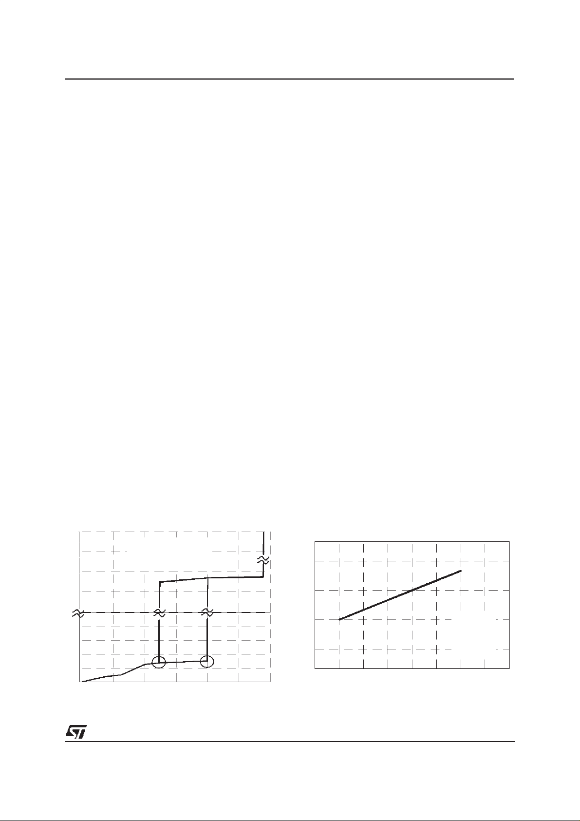
BLOCK DIAGRAM
RCT
3
DC
14
DIS
2.5V
13
ISEN
1.2V
SS
7
July 1999
+
-
-
+
OVER CURRENT
+
-
DIS
BLANKING
1V R
SYNC DC-LIM
TIMING2
T
PWM
FAULT
SOFT-START
2R
12
SGND COMP
25V
16V/10V
VREF OK
CLK
DIS
V
CC
Vref
+
PWM UVLO
-
SQ
R
2.5V
+
E/A
-
6
13V
VREF
48151
D98IN1002
9
V
C
10
OUT
11
PGND
5
VFB
1/24
L4990 - L4990A
ABSOLUTE MAXIMUM RATINGS
Symbol Parameter Value Unit
V
CC Supply Voltage (I
I
OUT
Output Peak Pulse Current 1.5 A
Analog Inputs & Outputs (6,7) -0.3 to 8 V
Analog Inputs & Outputs (1,2,3,4,5,15,14 13) -0.3 to 6 V
P
tot
T
j
T
stg
(*) maximum package power dissipation limits must be observed
Power Dissipation @ T
Junction Temperature, Operating Range -25 to 125
Storage Temperature, Operating Range -55 to 150
PIN CONNECTION
< 50mA) (*) selflimit V
CC
=70°C1W
amb
C
°
C
°
SYNC
RCT
DC
VREF
VFB
COMP
SS
V
CC
1
2
3
4
5
6
7 OUT
15
14
13
12
11
10
8V
D95IN197
N.C.16
DC-LIM
DIS
ISEN
SGND
PGND
9
C
THERMAL DATA
Symbol Parameter Value Unit
R
th j-amb
R
th j-amb Thermal Resistance Junction to Ambient
Thermal Resistance Junction to Ambient DIP16 80 °C/W
SO16
120 °C/W
PIN FUNCTIONS
N. Name Function
1 SYNC Synchronization. A synchronization pulse terminates the PWM cycle and discharges Ct
2 RCT Oscillator pin for external C
3 DC Duty Cycle control
4 VREF 5.0V +/-1.5% reference voltage
5 VFB Error Amplifier Inverting input
6 COMP Error Amplifier Output
7 SS Soft start pin for external capacitor Css
8V
9V
CC
C
Supply for internal ”Signal” circuitry
Supply for Power section
10 OUT High current totem pole output
11 PGND Power ground
12 SGND Signal ground
13 ISEN Current sense
14 DIS Disable. It must never be leftfloating. Tie to SGND if not used.
15 DC-LIM Connecting this pin to Vref, DC is limitedto 50%. If it is left floating or grounded no limitation is
imposed
16 NC Not connected
components
t,Rt
2/24
L4990 - L4990A
ELECTRICALCHARACTERISTICS
CC
= 15V; Tj=0 to 70°C; unless otherwisespecified.)
(V
Symbol Parameter Test Condition Min. Typ. Max. Unit
REFERENCE SECTION
V
O
T
S
Output Voltage Tj=25°C; IO= 1mA 4.925 5.0 5.075 V
Line Regulation V
Load Regulation I
= 12 to 20V 2.0 15 mV
CC
= 1 to 20mA 5.0 20 mV
O
Temperature Stability 0.4 mV/°C
Total Variation Line, Load,Temperature 4.875 5.0 5.125 V
I
OS
Short Circuit Current Vref = 0V 30 150 mA
Power Down/UVLO V
= 8.5V; I
CC
= 0.5mA 0.2 0.5 V
sink
OSCILLATOR SECTION
Initial Accuracy T
Accuracy R
Initial Accuracy T
Accuracy R
Duty Cycle pin 3 = 0,7V, pin 15 = Vref
Duty Cycle R
=25°C; RT= 4.42kΩ;
j
C
= 1nF; pin 15 Vref
T
= 4.42KΩ;VCC= 12 to 20V;
T
C
= 1nF; pin 15 = Vref
T
=25°C; RT= 4.42KΩ;
j
C
= 1nF; pin 15 OPEN
T
= 4.42KΩ;VCC= 12 to 20V;
T
C
= 1nF; pin 15 OPEN
T
pin 3 = 0.7V, pin 15 = OPEN
= 4.42kΩCT= 1nF
T
pin 3 = 3.2V, pin 15 = Vref
pin 3 = 3.2V, pin 15 = OPEN
285 300 315 kHz
279 300 321 kHz
280 295 310 kHz
275 295 315 kHz
0
0
45
90
Duty Cycle Accuracy pin 3 = 2.02V,pin 15 = OPEN 37 40 43 %
Oscillator Ramp Peak 3.0 V
Oscillator Ramp Valley 1.0 V
ERROR AMPLIFIER SECTION
Input Bias Current V
V
I
G
OPL
Input Voltage V
Open Loop Gain V
SVR Supply Voltage Rejection V
OL Output Low Voltage I
V
OH Output High Voltage I
V
I
O
Output SourceCurrent V
Output Sink Current V
to GND 0.2 1.0 µA
FB
COMP=VFB
= 2 to 4V 60 90 dB
COMP
CC = 12 to 20V 85 dB
= 2mA, VFB= 2.7V 1.1 V
sink
= 0.5mA, VFB= 2.3V 5 6 V
source
> 4V,VFB= 2.3V 0.5 1.3 mA
COMP
= 1.1V,VFB= 2.7V 2 6 mA
COMP
2.42 2.5 2.58 V
Unit Gain Bandwidth 2 4 MHz
S
R
Slew Rate 8 V/µs
PWM CURRENT SENSE SECTION
I
b
I
S
Input Bias Current I
Maximum Input Signal V
=0 3 15 µA
sen
= 5V 0.92 1.0 1.08 V
COMP
Delay to Output 100 ns
Gain 2.85 3 3.15 V/V
SOFT START
I
SSC
I
SSD
V
SSSAT
V
SSCLAMP
SS Charge Current 14 20 26
SS Discharge Current VSS = 0.6V 200
SS Saturation Voltage DC = 0% 0.6 V
SS Clamp Voltage 7 V
LEADING EDGE BLANKING
Internal Masking Time 100 ns
%
%
%
%
A
µ
A
µ
3/24
L4990 - L4990A
ELECTRICALCHARACTERISTICS
(continued.)
Symbol Parameter Test Condition Min. Typ. Max. Unit
OUTPUT SECTION
V
OL
V
OH
V
OUT CLAMP
Output Low Voltage IO= 250mA 1.0 V
Output High Voltage IO= 20mA; VCC= 12V 10 10.5 V
= 200mA; VCC= 12V 9 10 V
I
O
Output Clamp Voltage IO= 5mA; VCC = 20V 13 V
Collector Leakage V
Fall Time C
Rise Time C
UVLO Saturation V
CC = 20V VC = 24V 100 200 µA
= 1nF
O
C
= 2.5nF
O
= 1nF
O
C
= 2.5nF
O
CC =0VtoV
CCON;Isink
= 10mA 1.0 V
20
35
50
70
60 ns
100 ns
SUPPLY SECTION
V
CCON
V
CCOFF
V
hys Voltage AfterTurn-onHysteresis
I
S
I
op
I
q
I
SH
V
Z
Startup voltage
Minimum Operating Voltage L4990
Start Up Current Before Turn-on at:
Operating Current CT=1nF,RT=4.42kΩ,CO=1nF 12 18 mA
Quiescent Current (After turn on), Co =0nF
Shutdown Current 100 270 450
Zener Voltage I8= 20mA 21 25 30 V
V
=V
CC
C
= 1nF, RT= 4.42kΩ,
T
CCON
- 0.5V
L4990
L4990A157.8
9
L4990A
L4990
L4990A
7
5.5
0.5
100 270 450
16
8.4
10
7.6
17
9
11
8.2
6
0.8
7.0 10 mA
SYNCHRONIZATION SECTION
Master Operation
V
1
I
1
Clock Amplitude I
Clock Source Current Vclock = 3.5V 7 mA
= 0.8mA 4 V
SOURCE
Slave Operation
V
1
Sync Pulse Low Level 1 V
High Level 3.5 V
I
1
Sync Pulse Current VSYNC = 3.5V 0.8 mA
OVER CURRENT PROTECTION
V
t
Fault Threshold Voltage 1.1 1.2 1.3 V
DISABLE SECTION
Shutdown threshold 2.4 2.5 2.6 V
ns
ns
µ
µ
V
V
V
v
V
v
A
A
FUNCTIONAL DESCRIPTION
The I.C. contains a standard PWM current mode
control section with improved performance with
respectto the UC384Xfamily.
Enhanced features include start-up bias current
reduced to < 270µA (typ), improved E/A performance (4MHz B/W, 1.3mA Source Current, highslew rate) accurate 1MHz oscillator, and also reduced propagation delays in the critical path from
Current Sense to Output.
4/24
ADDITIONALFEATURES
SoftStart (SS)
An external capacitor is charged by an internal
constant current source (20µA) to generate a SS
signal which clamps the E/A output
The SS pin doubles as a Fault Reset Delay function as describedbelow.
Current Limit/ Reset Delay
An internal high-speed current limit comparator
L4990 - L4990A
referenced to 1.2V detects primary over-current
conditions. On detection of an overcurrent fault
the output is immediately shutdown and the fault
is also latched. A Fault Reset Delay is implemented by discharging the external Soft Start
(SS) timing capacitor before resetting the fault
latch and initiating a softstart cycle.
In case of a continuous fault condition the SS capacitor is charged to 5V before being discharged
again, to ensure that the fault frequency does not
exceed the programmedsoft start frequency.
Duty CycleLimit
A simple connectionbetween the DC-LIM and the
available Vref activatesan internal T- FlipFlop limiting the DC to about 50%. If this pin is not connected or grounded, the limit of the duty cycle is
extended to about 100%
Duty CycleControl
Duty Cycle DC is externally programmed by setting a voltage between 1V (0% DC) and 3V
(100% DC) at the DC pin. The programmed voltage is compared with the oscillator C
capacitor
T
charging waveform to determine the maximum
ON-time in each period. This function gives a fine
control of DC.
If this pin is floating the maximum duty cycle depends on DC-LIM status.
Synchronization
A SYNC pin eases Synchronization of the IC to
the external world ( e.g. another IC working in
parallelor to TV/monitorsyncsignal).
In TV/monitor applications the timing components
,CTare set for a frequency lower than the
R
T
minimum TV sync frequency.When the TV circuit
has powered-up it takes over and the system frequencyis that of the SYNC. Duty Cycle is controllableusing the DC function.
In parallel operation of several IC’s no Master/Slavedesignationis requiredas the higherfrequency IC is automaticallythe master. Controllers
to be synchronized have their SYNC pins tied together and each SYNC pin operatesas a bidirectional circuit. The first IC to drive its SYNC pin is
the master and it initiates a discharge of the C
timing capacitor of every controller. The Sync input signal is edge-triggered and sets an internal
”sync latch” which ensures full discharge of C
.
T
DisableFunction
The DIS pin performs a logic level latched-shutdown function. When pulled above 2.5V it shuts
down the complete IC with a standby current of
<270µA(typ).
To reset the IC the V
pin must be pulled-down
CC
belowthe lower UVLO threshold (10V).
LeadingEdge Blanking (LEB)
An LEB interval of 100ns has been incorporated
into the IC to blank out the current sense signal
during the first 100ns from switch turn-on.
This provides noise immunity to turn-on spikes
and reduces external RC filteringrequirementson
the current-sensesignal.
T
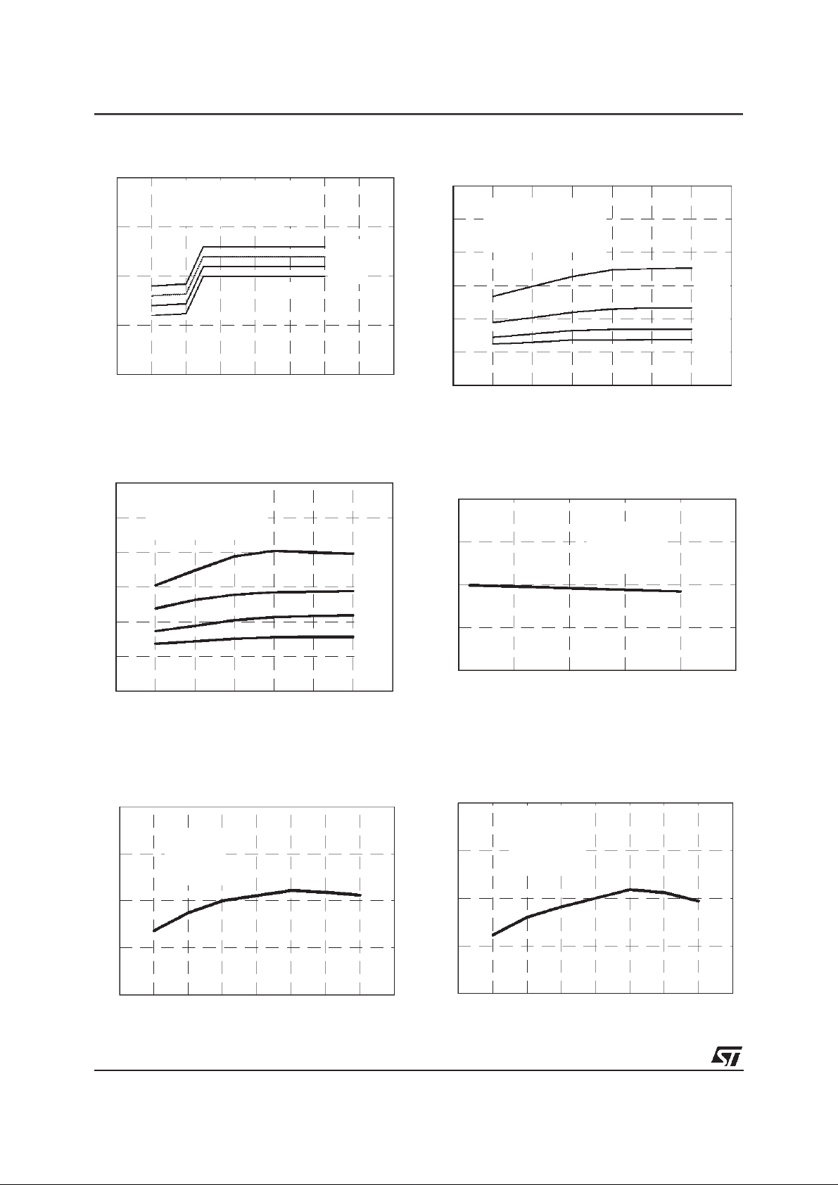
Figure 1. Quiescentcurrent vs. input voltage.
(X = 7.6V and Y = 8.4V for L4990A)
Iq [mA]
30
20
8
6
1
0.8
0.6
0.4
0.2
0
0 4 8 12162024
V14 = 0, OSC=disabled
Tj = 25°C
X
Vcc [V]
Y
Figure2. Quiescentcurrentvs. input voltage
(after disable).
Iq [uA]
300
270
240
210
8 1012141618202224
Vcc [V]
V14 = Vref
Tj = 25°C
5/24
L4990 - L4990A
Figure 3. Quiescentcurrent vs. input voltage.
Iq [m A ]
9.0
V14 = 0, V5 = Vref
8.5
8.0
7.5
7.0
8 1012141618202224
igure5. Quiescentcurrent vs. input voltage
F
Iq [mA]
36
30
24
Rt = 4 .5 Kohm ,Tj = 2 5°C
1M hz
500Khz
300Khz
100Khz
Vcc [V]
and switching frequency.
Co = 1nF, Tj = 25°C
DC = 100%
1MHz
igure4. Quiescentcurrentvs. input voltage
F
and switching frequency.
Iq [mA]
36
30
24
18
12
6
0
8 10121416182022
Co = 1nF, Tj = 25°C
DC = 0%
1MHz
500KHz
300KHz
100KHz
Vcc [V]
Figure6. Referencevoltage vs. load current.
Vref [V]
5.1
5.05
Vcc=15V
Tj = 25°C
18
12
500KHz
300KHz
100KHz
6
0
8 10121416182022
Vcc [V]
Figure 7. Vref vs. junction temperature.
Vref [V])
5.1
5.05
5
4.95
Vcc = 15V
Iref = 1mA
5
4.95
4.9
0 5 10 15 20 25
Iref [mA]
Figure8. Vref vs. junctiontemperature.
Vref [V]
5.1
Vcc = 15V
5.05
5
4.95
Iref= 20mA
4.9
-50 -25 0 25 50 75 100 125 150
Tj (°C)
6/24
4.9
-50 -25 0 25 50 75 100 125 150
Tj (°C)
L4990 - L4990A
Figure 9. Vref SVRR vs. switchingfrequency.
SVRR (dB)
120
80
40
0
1 10 100 1000 10000
fsw (Hz)
Vcc=15V
Vp-p=1V
Figure 11. Outputsaturation.
Vsat = V [V]
2.5
1.5
10
2
Vcc = 15V
Tj= 25°C
Figure10. Output saturation.
Vsat = V [V]
16
14
12
10
10
Vcc = 15V
Tj = 25°C
8
6
0 0.2 0.4 0.6 0.8 1 1.2
Isource [A]
Figure12. UVLO Saturation
Ipin10 [mA]
50
40
30
Vcc < Vccon
beforetu rn-on
1
0.5
0
0 0.2 0.4 0.6 0.8 1 1.2
Isink [A]
Figure13.Timingresistorvs.switchingfrequency.
fsw(KHz)
5000
2000
Vcc =15V,V15=0V
Tj= 25° C
1000
50 0
20 0
10 0
50
20
5.6nF
2.2nF
100p F
220pF
470pF
1nF
10
10 20 30 40
Rt (kohm)
20
10
0
0 200 400 600 800 1,000 1,200 1,400
Vpin10 [mV]
Figure14. Switchingfrequencyvs. temperature.
fsw (KHz)
320
Rt= 4.5Kohm, Ct = 1nF
310
300
290
280
-50 -25 0 25 50 75 100 125 150
Vcc = 15V, V15=Vref
Tj (°C)
7/24
L4990 - L4990A
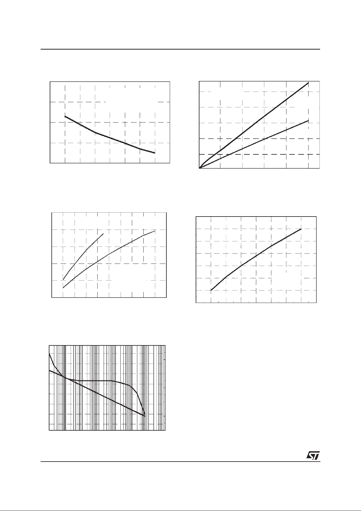
Figure 15. Switchingfrequencyvs. temperature.
fsw (KHz)
320
Rt= 4.5Kohm, Ct = 1nF
310
300
290
280
-50 -25 0 25 50 75 100 125 150
Vcc = 15V,V15= 0
Tj (°C)
Figure 17. Maximum Duty Cycle vs Vpin3.
DC ControlVoltage Vpin3 [V]
3.5
V15 = Vref
3
2.5
V15 = 0V
Figure16. Dead time vs Ct.
Dead time[ns]
1,500
Rt=4.5Kohm
V15= 0V
1,200
900
V15= Vref
600
300
246810
TimingcapacitorCt [nF]
Figure18.Delaytooutputvsjunctiontemperature.
Delayto output (ns)
130
120
110
100
2
Rt = 4.5Kohm,
1.5
Ct = 1nF
1
0 102030405060708090100
Duty Cy cle [%]
Figure 19. E/A frequencyresponse.
G [dB]
150
100
50
0
0.01 0.1 1 10 100 1000 10000 100000
f(KHz)
Phase
140
120
100
80
60
40
20
90
80
70
60
-50 -25 0 25 50 75 100 125 150
Tj(°C)
PIN10=OPEN
1Vpulse
onPIN13
8/24

L4990 - L4990A
APPLICATIONINFORMATION
Detailed Pin Functions Description
Pin 1. SYNC (In/Out Synchronization). This func-
tion allows the IC’s oscillator either to synchronize
other controllers(master) or to be synchronizedto
an externalfrequency(slave).
As a master, the pin delivers positive pulses during the ramp-down of the oscillator (see pin 2). In
slave operationthe circuitis edgetriggered. Refer
to fig. 21 to see how it works. When several IC
Figure 20. Synchronizingthe L4990.
SYNCSYNC
1
L4990 L4990
VREF
4
2
R
T
C
T
(a) (b) (c)
1
2
RCTRCT
R
OSC
L4981A
(MASTER)
16
1817
C
OSC
work in parallel no master-slave designation is
needed because the fastest one becomes automaticallythe master.
During the ramp-up of the oscillator the pin is
pulled low by a 600µA generator. During the
ramp-down, that is when the pulse is released,
the 600µA pull-downis disconnected.The pin becomes a generator whose source capability is
typically 7mA (with a voltage still higher than
3.5V).
In fig. 20, some practical examplesof synchroniz-
ing the L4990 are given.
R
T
VREF
L4990
(SLAVE)
1
VREFSYNC
4
2
RCT
RCT
R
T
C
C
T
T
D97IN494A
4
L4990
(MASTER)
SYNC
12
SYNC
R
L4981A
(SLAVE)
16
OSC
17 18
C
OSC
Pin 2.
pacitor (C
operating frequency f
C
RCT (Oscillator). A resistor (R
), connectedas shown in fig. 21 set the
T
is charged through RTuntil its voltage reaches
T
of the oscillator.
osc
) and a ca-
T
3V, then is quickly internally discharged. As the
voltage has dropped to 1V it starts being charged
again
Figure 21. Oscillator and synchronizationinternalschematic.
V
4
REF
R1
CLAMP
R
T
RCT
2
D1
C
T
50Ω
R2R3
+
-
SYNC
1
600µA
D97IN500B
D
R
CLK
Q
9/24

L4990 - L4990A
The frequency can be established with the aid of
fig. 13 diagrams or considering the approximate
relationship:
1
⋅ (0.693 ⋅ RT+ K
= VREF
15
= GND/OPEN
15
(1)
T)
(2)
where K
≅
f
osc
C
T
is defined as:
T
90, V
=
K
T
160 V
and is linked to the duration of the falling edge of
the sawtooth:
≅ 30 ⋅ 10-9+KT⋅CT(3)
T
d
T
is also the duration of the sync pulses deliv-
d
ered at pin 1 and defines the upper extreme of
the duty cycle range, D
(seepin 15 for Dxdefini-
x
tion and calculation).
In case V
is connected to VREF, however, the
15
switching frequency of the system will be as
high as half f
osc
.
If the IC is to be synchronizedto an externaloscillator, R
and CTshould be selected for a f
T
osc
lower than the master frequency in any condition
(typically, 10-20% ), depending on the tolerance
and CTitself.
of R
T
Pin 3. DC (Duty Cycle Control). By biasing this
pin with a voltagebetween 1 and 3 V it is possible
to set the maximumduty cycle between 0 and the
upper extremeD
If D
is the desired maximum duty cycle, the
max
(seepin 15).
x
voltage V3 to be appliedto pin 3 is:
(2-Dmax)
=5-2
V
3
is determined by internal comparison be-
D
max
(4)
tween V3 and the oscillator ramp (see fig. 22),
thus in case the device is synchronized to an external frequency f
(and therefore the oscillator
ext
amplitude is reduced),(4) changesinto:
= 5− 4 ⋅ exp
V
3
D
−
max
⋅ CT⋅
R
T
(5)
f
ext
A voltage below 1V will inhibit the driver output
stage. This could be used for a not-latcheddevice
disable, for example in case of overvoltage protection (seeapplication ideas).
If no limitation on the maximum duty cycle is required (i.e. D
MAX=DX
), the pin has to be left floating. An internal pull-up holds the voltage above
3V. Should the pin pick up noise (e.g. during ESD
tests), it can be connected to V
REF
through a
4.7kΩresistor.
Figure22. Duty cycle control.
V
REF
4
R1
DC
3
R2
R
Pin 4.
T
RCT
2
C
T
VREF (Reference Voltage). An internal
TO PWM LOGIC
+
-
D97IN501A
generatorfurnishesan accurate voltage reference
(5V±1.5%) that can be used to supply an external
circuit(consider some ten mA).
A small film capacitor (1 µF typ.), connected between this pin and SGND, is recommended to
preventswitchi ngnoise from affectingtherefer enc e.
Beforedeviceturn-on,thispinhasa sink currentcapabilityof 0.5mA.
Pin 5. VFB (Error Amplifier Inverting Input). The
feedback signal is applied to this pin and is compared to the E/A internal reference (2.5V). The
E/A output generates the control voltage which
fixesthe duty cycle.
The E/A features high gain-bandwidth product,
which allows to broaden the bandwidth of the
overall control loop, high slew-rate and current
capability, which improves its large signal behavior. Usually the compensationnetwork, which stabilizes the overall control loop, is connected between this pin and COMP (pin 6).
Pin 6.
COMP (Error Amplifier Output). Usually,
this pin is used for frequency compensation and
the relevant network is connected between this
pin and VFB (pin 5). Compensation networks towards ground are not possible since the L4990
E/A is a voltage mode amplifier (low output impedance). See application ideas for some example of compensationtechniques.
Pin 7.
SS (Soft-Start). At device start-up, a capacitor (Css) connected between this pin and
SGND (pin 12) is charged by an internal current
generator, ISSC, up to about 7V. During this
ramp, the E/A output is clamped by the voltage
across Css itself and allowedto rise linearly,starting from zero, up to the steady-state value imposed by the control loop. The maximum time intervalduring which the E/A is clamped, referred to
as soft-starttime,is approximately:
10/24

L4990 - L4990A
3 ⋅ R
≅
T
ss
where R
13) and I
through R
is the current sense resistor(see pin
sense
is the switch peak current (flowing
Qpk
sense
load. Usually, C
), which depends on the output
SS
⋅ I
sense
I
SSC
Qpk
⋅
C
ss
(6)
is selected for a TSSin the or-
der of milliseconds.
Figure 23. Regulationcharacteristicandre-
lated quantities
V
OUT
D.C.M. C.C.M.
T
ON
D97IN495
A
D
I
SHORTIOUT(max)
B
I
Qpk
1-2 ·I
I
Qpk(max)
C
T
ON(min)
I
OUT
Figure 24. Hiccup mode operation.
Qpk
As mentioned before, the soft-start intervenes
also in case of severe overload or short circuit on
the output. Referring to fig. 23, pulse-by-pulse
current limitation is somehoweffective as long as
the ON-time of the power switch can be reduced
(from A to B). After the minimum ON-time is
reached (from B onwards) the current is out of
control.
To prevent this risk, a comparator trips an overcurrent handling procedure, named ’hiccup’ mode
operation, when a voltageabove 1.2V (point C) is
detected on current sense input (ISEN, pin 13).
Basically,the IC isturned off and then soft-started
as long as the fault condition is detected. As a result, the operating point is moved abruptly to D,
creating a foldback effect. Fig. 24 illustrates the
operation.
The oscillation frequency appearing on the softstart capacitor in case of permanent fault, referred
to as ’hiccup” period, is approximatelygiven by:
4.5
⋅
I
SSC
≅
T
hic
1
1
I
SSD
⋅
(7)
C
ss
+
Since the system tries restarting each hiccup cycle, there is not any latchoff risk.
I
OUT
I
SEN
FAULT
SS
5V
0.5V
SHORT
7V
T
hic
D97IN496
time
11/24

L4990 - L4990A
Figure25.Turn-onandturn-offspeedsadjustment
Rg’
V
DRIVE &
CONTROL
L4990
D97IN497A
V
PGND
C
9
(V)
17
13
10
OUT
11
Rg
CC
8
13V
Rg(ON)=Rg+Rg’
Rg(OFF)=Rg
”Hiccup” keeps the system in control in case of
short circuits but does not eliminate power components overstress during pulse-by-pulse limitation (from A to C). Other external protection circuits are needed if a better control of overloadsis
required.
Pin 8.
VCC (Controller Supply). This pin supplies
the signal part of the IC. The device is enabledas
VCC voltage exceeds the start threshold and
works as long as the voltage is above the UVLO
threshold. Otherwise the device is shut down and
the current consumptionis extremelylow.
An internal Zener limits the voltage on VCC to
25V. Below this value the IC current consumption
is lowbut increasesconsiderablyif this limit is exceeded.
A small film capacitor between this pin and SGND
(pin 12), placed as close as possible to the IC, is
recommendedto filterhigh frequencynoise.
delivers a voltage internally clamped,as shown in
fig. 25. Thus it is possible to supply the driver (pin
9) with higher voltages without any problem of
damage for the gate oxide of the external MOS,
but, of course,the power dissipation on theIC will
increase.
In UVLO conditions an internal circuit (shown in
fig.26) holds the pin low in order to ensure that
the external MOS cannot be turned on accidentally. The peculiarity of this circuit is its ability to
mantain the same sink capability (typically, 20mA
@ 1V) from V
= 0V up to the start-upthreshold.
CC
When the threshold is exceeded and the L4990
starts operating, V
REFOK
is pulled high (refer to
fig. 26) and the circuitis disabled.
It is then possible to omit the ”bleeder” resistor
(connected between the gate and the source of
the MOS) ordinarily used to prevent undesired
switching-on of the external MOS because of
someleakage current.
Figure26. Pull-Down of theoutput in UVLO.
OUT
10
V
REFOK
12
SGND
D97IN538
Pin 9. VC (Supply of the Power Stage). It supplies the driver of the external switch and therefore absorbs a pulsed current. Thus it is recommended to place a buffer capacitor (towards
PGND, pin 11, as close as possible to the IC)
able to sustain these current pulses and in order
to avoid them inducing disturbances.
This pin can be connected to the buffer capacitor
directly or through a resistor, as shown in fig. 25,
to control separately the turn-on and turn-off
speed of the external switch, typically a PowerMOS. At turn-on the gate resistance is R
g
+R
and turn-offis Rgonly.
Pin 10.
OUT (Driver Output). This pin is the output of the driver stage of the external power
switch. Usually, this will be a PowerMOS, although the driver is powerful enough to drive
BJT’s (1.6A source,2Asink,peak).
The driver is made up of a totempole with a highside NPN Darlington anda low-side VDMOS, and
12/24
Pin 11.
PGND (Power Ground). The current loop
during the discharge of the gate of the external
MOS is closed through this pin. This loop should
be as short as possible to reduce EMI and run
separatelyfrom signal currentsreturn.
Pin 12
. SGND (Signal Ground). This ground references the control circuitry of the IC, so all the
ground connections of the external parts related
to control functions must lead to thispin. In laying
out the PCB, care must be taken in preventing
switched high currents from flowing through the
g’
SGND path.
Pin 13. ISEN (Current Sense). This pin is to be
connected to the ”hot” lead of the current sense
resistor R
(being the other one grounded),to
sense
get a voltage ramp which is an image of the current of the switch, (I
). When this voltage is equal
Q
to:

L4990 - L4990A
V
13pk
=
⋅
I
R
Qpk
sense
(V
=
COMP
− 1.4)
3
the conductionof the switch is terminated.
Figure 27. Internal LEB
I
3V
0
ISEN
13
1.2V
+
-
FROM E/A
OVERCURRENT
COMPARATOR
(8)
CLK
To increase the noise immunity, a ”Leading Edge
Blanking” of about 100ns is internally realized as
shown in fig. 27. Because of that, the smoothing
RC filter between this pin and R
sense
movedor, at least,considerablyreduced.
2V
+
-
PWM
COMPARATOR
+
-
D97IN503
TO
LOGIC
TO
LOGIC
PWM
FAULT
could be re-
Pin 14.
DIS (Device Disable). When the voltage
on pin 14 rises above 2.5V the IC is shut down
and it is necessary to pull VCC (IC supply voltage, pin 8) below the UVLOthresholdto allow the
device to restart. When disabled, the current consumption of the IC is as low as beforestart-up.
The pin can be driven by an external logic signal
in case of power management, as shown in fig.
28. It is also possible to realize an overvoltage
protection, as shown in the section ” Application
Ideas”.
If used, bypass this pin to groundwith a filter capacitor to avoid spurious activation due to noise
spikes. If not, it is advisable to connect the pin to
SGND, even though it might be left floating.
Pin 15.
DC-LIM(Maximum Duty Cycle Limit). The
upper extreme, Dx, of the duty cycle range depends on the voltage applied to this pin. Approximately,
R
T
D
x
≅
RT+ 230
(
9)
if DC-LIM is grounded or left floating. Instead,
connecting DC-LIM to VREF (half duty cycle option), Dx will be set approximately to:
R
≅
D
x
2 ⋅ RT+ 260
T
(10)
Figure28. Disable (Latched)
DISABLE
SIGNAL
DIS
14
+
-
C
2.5V
D
R
UVLO
Q
DISABLE
D97IN502
and the output switching frequency will be halved
with respect to the oscillator one because an internal T flip-flop (see block diagram, fig. 1) is activated.Fig. 29 shows the operation.
The half duty cycle option speeds up the discharge of the timing capacitor C
(in order to get
T
duty cycles as close as possible to 50%) so the
oscillator frequency - with the same R
and CT-
T
will be slightly higher.
The halving of frequency can be used to reduce
losses at light load in all those systems that must
comply with requirements regarding energy consumption (e.g.monitor displays).
13/24

L4990 - L4990A
Figure 29. Half dutycycle option.
V15=GND
V5=V13=GND
t
d
V2
D
X
=
t
c
tc+t
d
t
c
t
d
V15=VREF
V5=V13=GND
t
c
DEMONSTRATION BOARD
To evaluate the device performance, a demonstration board has been realized. Despite its simplicity, it exploits most of the features of the
L4990.
The board embodies an applicationbased on the
following specification of universal mains AC-DC
adapter:
Inputvoltage range: 85-270 Vac (50/60 Hz)
Outputvoltage:15 V
Outputcurrent:0.5 to 2A
Outputvoltage ripple : 300 mV (max.)
Load regulation: ± 5%(0.5 to 2 A load change)
Target efficiency @ Iout = 2 A: ; 80% over the
input voltagefull range
Some preliminary decisions, concerning topology,
operating mode, switching frequency, maximum
duty cycle allowed and control technique, have
been made.
As for topology, at this power level and output
voltage, flyback is the most advantageous one,
mainly because of its simplicity, which means low
parts count,low cost and inherent high efficiency.
A peculiar design choice aiming at optimizing the
overall system concerns the operating mode: the
converter will work in continuouscurrent mode at
low input voltages, when input current is greater,
and in discontinuous mode at higher input volt-
V10
V2
t
c
2·tc+t
d
D97IN498
V10
D
=
X
ages.Numerous benefits originate from that.
Compared to discontinuous current mode, con-
tinuous operation involves lower peak currents
(typ. -40%) at the same throughput power. This
implies less stress for all powercomponents.
The transformer inductance is higher and, therefore, a smallerair gap is required for a given core:
this increasesprimary-to-secondary coupling and,
as a consequence, reduces leakage inductance
and improves energy transfer. Both efficiency and
load regulation will take advantage of that.
Another point in favor is a reduction of the minimum output power that the system is able to deliver keeping the output well regulated.
Few components are required in addition for
slope compensation.
Actually, continuous mode flyback suffers also
from a poor dynamic behavior during load transients because of the narrow bandwidth of the
control loop due to stability problems. However,
great dynamic performance is not required to ACDC adapters,so this problem is of no concern.
The boundary between the two operating modes
has been set at about 150 Vac (@ Iout=2A).
The selection of the switching frequency is a matter of trade-off between achieving a small transformersize and high efficiency. 200 kHz seems to
be a goodcompromise.
In this application, the wide input voltage range
requires a large duty cycle sweep. The higher is
the maximum duty cycle, the larger is the operat-
14/24

L4990 - L4990A
ing conditionsrange, in termsof input voltageand
output current, that the converter is able to cover
but, on the other hand, the higher is the peak current on the secondary side.
As to this point, the L4990 turns out to be particularly useful since it allows to set any maximum
duty cycle greater (and lower) than 50% with very
good precision. In the present case, a maximum
duty cycle of 60% for steady state operation has
been selected and an extra 5% is allowed to take
transients into account.
Since it is not requested a very tight tolerance on
the output, the feedback employs a primary side
voltage sensing technique to reduce cost and
complexity of the circuit. The same technique has
been used to protect against outputovervoltages.
The electric schematic is shown in fig. 30. The
PCB layout is shown in figg. 31 and 32. Table 1
and 2 summarize typical system performance,
while table 3 lists the relevant bill of material,
where details are given only for critical components and/orwhereuseful.
Warning:
the NTC for inrush current limitation is
not assembled,thus use caution when connecting
the demo board to the mains directly. The use of
a variac or an isolation transformer is recommended.
Table 1. System efficiency.
I
=1A I
(Vac) V
V
in
out
(V) Effic. % V
out
out
(V) Effic. %
out
85 14.93 83.7 14.53 84.3
110 14.95 82.5 14.55 84.9
220 14.95 81.4 14.57 85.2
270 14.96 76 14.59 81.6
Table 2. System performance.
Line regulation Vin= 85 to 270 Vac
Load regulation
I
= 0.5A to 2A
out
Maximum effic. V
Output ripple V
Minimum load V
Transition Volt. From C.C.M to D.C.M
I
= 0.5A
out
= 85 Vac
V
in
V
= 270 Vac
in
= 190 Vac
in
I
=2A
out
= 85 to 270 Vac
in
I
=2A
out
= 270 Vac
in
V
< 20V
out
I
=2A
out
=2A
30mV
0.95V
0.90V
86.2%
< 200mV
150mA
160V
Figure 30. AC-DC adaptor electric schematic
NTC
L4990
7
DC-LIM SGND
C5 C6
B1
C1
R15R2
R6
8146
1512
C15
R12 R19C8
R13
C3
R3
VCVCCDISCOMPVFB
OUT
10
ISEN
13
11
PGND
R23
C14
85
to
270
Vac
R1
R5
R8
C4
DCC
R9
VREF
R10
C10
R4
C7
59
3
4
2
RCT SS
Q2
R22
R20
R21
C11
R7
R24
C12
R16
T1
D4
D3
D2R14
Q1
R11
D1
C2
C13
D97IN499B
15V/2A
R17
GND
15/24

L4990 - L4990A
Table 3. Components List of the Fig. 30 AC-DCadaptorelectricschematic.
Component Reference Value Description
Resistors R1 1.6k
R2 9.1kΩ 2%, 1/8W
R3, R14 10Ω 5%, 1/8W
R4 360kΩ 2%, 1/8W
R5 27kΩ 2%, 1/8W
R6 200kΩ 2%, 1/8W
R7 4.7Ω 2%, 1/8W
R8, R9 4.7k
R10 5.6k
R11 1
R12, R13 24k
R15 330Ω 5%, 1/8W
R16 - Not used
R17 390Ω 5%,1W, 2 paralleled resistors (not used)
R19 100kΩ 5%, 1W
R20, R21 470kΩ 2%, 1/8W
R22 200Ω 5%, 1/8W
R23 2k
R24 1k
Capacitors C1 100µF 400V, NCC-SMH or equiv.
C2 330µF 25V, NCC-LXF or equiv., 3 paralleled capacitors
C3 47µF 25V, electrolytic
C4 1µF 10V,electrolytic
C5 1nF J precision
C6, C15 10nF
C7, C14 330pF
C8 330pF 160V, polypropilene
C9 100nF
C10 220nF
C11 100pF ceramic
C12 - Not used
C13 4.7nF 630V
Transformer T1 380µH Core: EFD25, Philips, 3F3 ferrite (or equivalent)
Transistors Q1 STP5NA80 ST, TO220 package
Q2 2N2222 ST (or equivalent)
Diodes B1 DF04M GI (or equivalent)
D1 STPS20100CT ST, Shottky, TO220 package
D2, D3 1N4148 ST (or equivalent)
D4 BYT11-600 ST, F126 package
Fuse Fuse T2A250V ELU (or equivalent)
NTC NTC - Not used (see warning)
Ω
Ω
Ω
Ω
Ω
Ω
Ω
2%, 1/8W
2%, 1/8W
2%, 1/8W
2%, 1/2W, metallic film (low inductance)
2%, 1/2W
2%, 1/8W
5%, 1/8W
Primary: 46 T, litzwire 20 x 0.1, interleaved assembly
Secondary: 6 T, 4 paralleled litz wire 20 x 0.1
Auxiliary: 7 T (evenly spaced), ∅ 0.2 mm GAP ~ 0.7mm
16/24

Figure 31. AC-DC adaptor PCB layout (1.25 :1 scale) - Component Side.
L4990 - L4990A
Figure 32. AC-DC adaptor PCB layout (1.25 :1 scale) - Back Side.
17/24

L4990 - L4990A
Layout hints.
Generally speaking a proper circuitboard layout is vital for correct operation but is
not an easy task. Careful component placing, correct traces routing, appropriate traces widths and,
in case of high voltages,compliancewith isolation
distances are the major issues. The L4990 eases
this task by putting two pins at disposal for separate current returns of bias (SGND) and switch
drive currents (PGND) The matter is complexand
only fewimportant points will be herereminded.
1) All current returns (signal ground, power
ground, shielding, etc.) should be routed separately and should be connectedonly at a single
groundpoint.
2) Noise coupling can be reduced by minimizing
and the inductance of the wiring.
4) Magnetic field radiation (and stray inductance)
can be reduced by keeping all traces carrying
switchedcurrents as short as possible.
5) In general, traces carrying signal currents
should run far from traces carrying pulsed currents or with quickly swinging voltages. From
this viewpoint, particular care should be taken
of the high impedance points (current sense input, feedback input, ...). It could be a good idea
to route signal traces on one PCB side and
power traceson the other side.
6) Provide adequate filtering of some crucial
points of the circuit, such as voltage references, IC’s supplypins, etc.
the area circumscribed by current loops. This
applies particularly to loops where high pulsed
currentsflow.
3) For high current paths, the traces should be
doubled on the other side of thePCBwhenever
possible: this will reduce both the resistance
APPLICATION IDEAS
Herefollows a seriesofideas/suggestionsaimedat
either improving performance or solving common
applicationproblems of L4990-basedsupplies.
Figure 33. Isolated MOSFET Drive & Current TransformerSensing in 2-switch Topologies.
V
ISOLATION
V
C
9
BOUNDARY
IN
10
L4990
13
1112
PGND
SGND
Figure 34. Low consumption start-up
2.2MΩ 33KΩ
22V
V
47KΩ
REF
OUT
ISEN
V
IN
STD1NB50-1
8
4
L4990
12 11
D97IN504
T
V
CC
SELF-SUPPLY
WINDING
18/24
D97IN505A

Figure 35. Bipolar Transistor Drive
V
8
L4990
CC
11
V
C
9
PGND
Figure 36. Typical E/A compensationnetworks.
10
13
OUT
ISEN
D97IN506
L4990 - L4990A
V
IN
From V
O
2.5V
+
1.3mA
R
i
VFB
R
C
d
f
R
f
COMP
+
5
EA
6
2R
R
12
SGND
Error Amp compensation circuit for stabilizing any current-mode topology
except
for boost and flyback converters operating with continuous inductor current.
EA
+
1.3mA
2R
12
R
SGND
D97IN507
From V
R
P
C
P
O
R
i
C
R
d
f
VFB
R
COMP
2.5V
+
5
-
f
6
Error Amp compensation circuit for stabilizing current-mode boost and flyback
topologies operating with continuous inductor current.
19/24

L4990 - L4990A
Figure 37. Feedback with optocoupler
COMP
6
L4990
V
OUT
5
VFB
Figure 38. Slope compensationtechniques
V
REF
4
R
T
RCT
2
C
R
I
R
SLOPE
SENSE
T
ISEN
OPTIONAL
13
L4990
12
SGND
I
R
SLOPE
R
SENSE
R
T
OPTIONAL
V
REF
RCT
C
T
ISEN
TL431
D97IN508
4
2
L4990
13
12
SGND
SGND
D97IN509A
L4990
12
10
13
OPTIONAL
OUT
ISEN
RR
R
SLOPE
C
R
SLOPE
SENSE
Figure 39. Protection against overvoltage/feedbackdisconnection (latched)
20/24
DIS
R
START
V
CC
8
14
L4990
12 11
SGND
PGND
D97IN510
V
Z
2.2K
DIS
R
START
V
CC
14
L4990
12 11
SGND
8
PGND
D98IN904

L4990 - L4990A
Figure 40. Protection against overvol-
Figure41. Device shutdown on overcurrent
tage/feedbackdisconnection(not
latched)
I
≅
R
1
D97IN512A
pk max
R
2
VREF
DC
4
3
R
START
V
12
CC
8
L4990
11
D97IN511A
PGND
L4990
SGND
1211
4
14
13
OPTIONAL
VREF
DIS
ISEN
Figure 42. Constant power in pulse-by-pulsecurrentlimitation(flybackdiscontinuous)
V
IN
80 ÷
PGND
400V
L4990
DC
OUT
SGND
10
R
FF
ISEN
13
1211
L
p
R·L
p
RFF= 5·10
R
R
SENSE
6
R
SENSE
R
R
SENSE
2.5
SENSE
I
R
2
1-
•
R
1
I
pk
D97IN513
Figure 43. Voltage mode operation.
DC
3
10K
COMP
6
L4990
12 13
SGND ISEN
D97IN570A
REFERENCES
[1] EfficientactiveClamp for Off-line ApplicationsusingL4990and L6380 (N.Tricomi, G. Gattavari,
C. Adragna, PCIM96 - NURBERG).
[2] 25WOff-Line AutorangingBattery Charger with L4990 (AN889)
[3] 300WSecondary Controlled Two-SwitchForwardConverter with L4990 (AN890)
[4] SMPSwith L4990 for Multisync Monitors(AN891)
[5] HighperformanceVRM using L4990A,for Pentium Pro processor(AN908).
21/24

L4990 - L4990A
DIM.
MIN. TYP. MAX. MIN. TYP. MAX.
a1 0.51 0.020
B 0.77 1.65 0.030 0.065
b 0.5 0.020
b1 0.25 0.010
D 20 0.787
E 8.5 0.335
e 2.54 0.100
e3 17.78 0.700
F 7.1 0.280
I 5.1 0.201
L 3.3 0.130
Z 1.27 0.050
mm inch
OUTLINE AND
MECHANICAL DATA
DIP16
22/24

L4990 - L4990A
DIM.
MIN. TYP. MAX. MIN. TYP. MAX.
A 2.35 2.65 0.093 0.104
A1 0.1 0.3 0.004 0.012
B 0.33 0.51 0.013 0.020
C 0.23 0.32 0.009
D 10.1 10.5 0.398 0.413
E 7.4 7.6 0.291 0.299
e 1.27 0.050
H 10 10.65 0.394 0.419
h 0.25 0.75 0.010 0.030
L 0.4 1.27 0.016 0.050
K0°(min.)8° (max.)
mm inch
0.013
OUTLINE AND
MECHANICAL DATA
SO16 Wide
L
A
B
D
16
1
e
9
E
8
K
hx
H
45
A1
C
23/24

L4990 - L4990A
Information furnished is believed to be accurate and reliable. However, STMicroelectronics assumes no responsibility for the consequences
of use of such information nor for any infringement of patents or other rights of third parties which may result from its use. No license is
granted by implication or otherwise under any patent or patent rights of STMicroelectronics. Specification mentioned in this publication are
subject to change without notice. This publication supersedes and replaces all information previously supplied. STMicroelectronics products
are not authorized for use as critical components in life support devices or systems without express written approval of STMicroelectronics.
The ST logo is a registered trademark of STMicroelectronics
1999 STMicroelectronics – Printed in Italy – All Rights Reserved
STMicroelectronics GROUP OF COMPANIES
Australia - Brazil - China - Finland - France - Germany - Hong Kong - India - Italy - Japan - Malaysia - Malta - Morocco -
Singapore - Spain - Sweden - Switzerland - United Kingdom - U.S.A.
http://www.st.com
24/24
 Loading...