

Datasheet L4987CPT87, L4987CPT120, L4987CPT50, L4987CPT30 Datasheet (SGS Thomson Microelectronics)
L4987
VERY LOW DROP VOLTAGE REGULATORS
WITH INHIBIT AND DROPOUT CONTROLFLAG
■ VERYLOWDROPOUTVOLTAGE(0.25V
TYP.)
■ DROPOUTCONTROLFLAG
■ VERYLOW QUIESCENTCURRENT
(TYP.90 µA IN OFF MODE,500µAINON
MODE)
■ OUTPUT CURRENT UP TO200 mA
■ LOGIC-CONTROLLEDELECTRONIC
SHUTDOWN
■ OUTPUT VOLTAGESOF 3V,5V 8.7V 12V
■ INTERNAL CURRENTAND THERMAL LIMIT
■ ONLY2.2µF FORSTABILITY
■ AVAILABLEIN ± 2%SELECTIONAT25
■ SUPPLYVOLTAGEREJECTION:70 dB (TYP.)
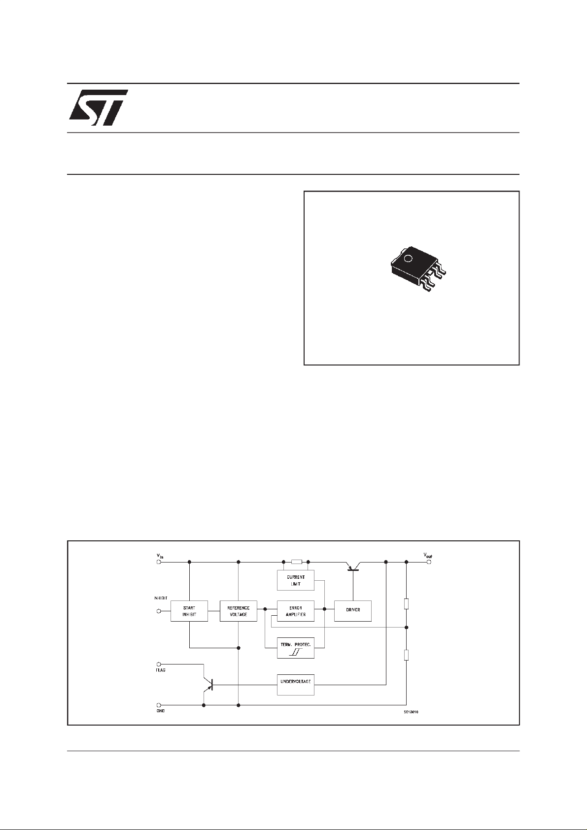
DESCRIPTION
The L4987 is a very low drop regulatoravailable
in PPAK. The very low drop-voltage(0.5V Max at
200 mA) and the very low quiescent currentmake
it particularly suitable for low noise, low power
applications,and in battey powered systems. The
input dump protection up to 40V makes it ideal for
automotive applications. a shutdown Logic
Control function is available (pin2, TTL
compatible). This means that when the device is
used as a local regulator, it is possible to put a
o
C
SERIES
PPAK
part of the boad in standby, decreasing the total
power consumption. The regulator employs an
output pin (open collector) providing a logic signal
when the pass transistor is in saturation at low
input voltage, this signal can be used to prevent
the pop-up phenomenon in the car radio. In
battery powered systems (the cellular phone,
notebook) it is possible to use the flag to monitor
the battery charge status through the dropout of
the regulator.
SCHEMATIC DIAGRAM
October 1998
1/11
L4987 SERIES
ABSOLUTE MAXIMUM RATINGS
Symbol Parameter Value Unit
V
DC Input Voltage 40 V
i
OutputCurrent Internally limited mA
I
o
PowerDissipation Internally limited mW
P
tot
Storage Temperature Range - 40 to 150
T
stg
OperatingJunctionTemperatureRange - 40 to 125
T
op
Absolute Maximum Rating are those values beyond wich damage to the device may occur. Functional operation under these conditions is
not implied.
THERMALDATA
Symbol Parameter DPAK/PPAK Unit
R
thj-cas e
R
thj-amb
Thermal Resistance Junction-case
Thermal Resistance Junction-ambient
8
100
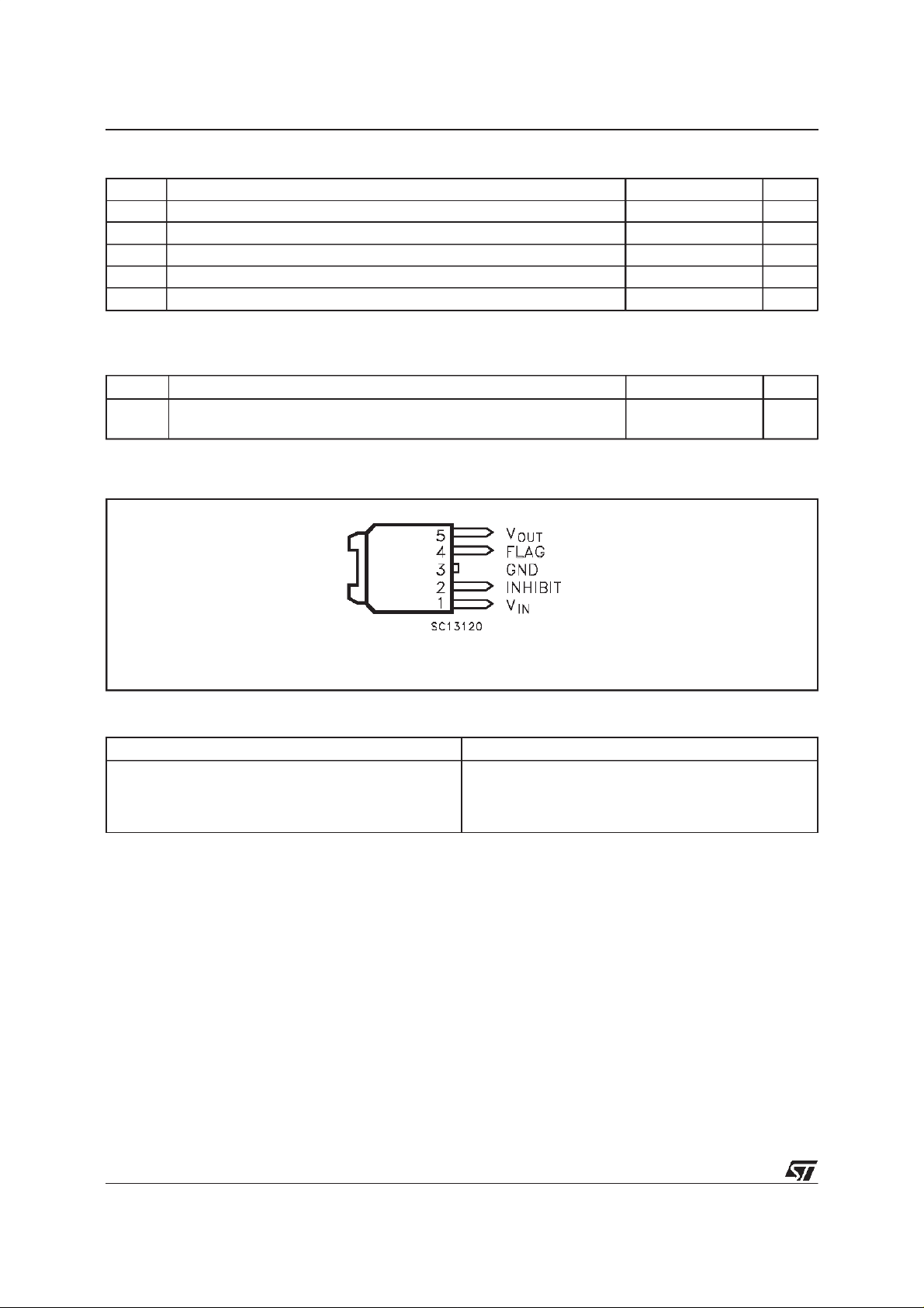
CONNECTION DIAGRAM (top view)
o
o
o
C/W
o
C/W
C
C
ORDERING NUMBERS
L4987CPT30(*)
L4987CPT50(*)
L4987CPT87(*)
L4987CPT120(*)
(*) Available even in tape& reel
2/11
Type Output Voltage
3V
5V
8.7 V
12 V

L4987 SERIES
ELECTRICAL CHARACTERISTICS FOR L4987CPT30
= 5 mA, Tj=25oC, Ci= 0.1 µF, Co= 2.2 µF unless otherwisespecified)
I
OUT
(refer to the test circuits, V
=6V,
I
Symbol Parameter Test Conditions Min. Typ. Max. Unit
OutputVoltage Io=200 mA, Vi=6V
V
I
∆
∆V
o
OperatingInput Voltage Io=200 mA 3.62 18 V
V
i
OutputCurrentLimit 250 A
out
LineRegulation Vi= 4.3to 18 V, Io=0.5mA 2.4 14 mV
V
o
LoadRegulation Vi= 4.1V Io= 0.5to 200 mA 3 20 mV
o
Quiescent Current ON MODE
I
d
=200 mA, Vi= 6 V -40<TJ<125oC
I
o
= 4.3to 18 V Io=0mA
V
i
= 4.3to 18 V Io=200 mA
V
i
OFF MODE V
SVR Supply VoltageRejection
=5 mA Vi=5.3V±1V
I
o
f = 120Hz
f=1KHz
f = 10KHz
Dropout Voltage Io=200 mA
V
d
Control Input Logic Low -40< TJ< 125oC0.8V
V
il
Control Input Logic High -40 < TJ< 125oC2 V
V
ih
Control Input Current 10
I
i
OutputBypassCapacitance
C
O
=200 mA -40< TJ<125oC
I
o
ESR = 0.5 to 10ΩI
-40 < T
Control Flag OutputLow Vi-Vo<V
V
fl
Control Flag OutputHigh
I
fh
I
=200 mA
o
Vi> 3.62V Voh=15V 10 µA
i
< 125oC
J
power, Ifl=6mA
cesat
2.94
2.88
=12V 90 180
= 0 to 200mA
o
210
33.06
3.12
0.7
1.5
1
6
80
75
60
0.25 0.5
0.7
0.5 V
Leakage Current
V
V
mA
mA
A
µ
dB
dB
dB
V
V
A
µ
F
µ
3/11

L4987 SERIES
ELECTRICAL CHARACTERISTICS FOR L4987CPT50
= 5mA, Tj=25oC, Ci= 0.1 µF, Co= 2.2 µF unless otherwise specified)
I
OUT
(refer to the test circuits, V
=8V,
I
Symbol Parameter Test Conditions Min. Typ. Max. Unit
OutputVoltage Io=200 mA, Vi=8V
V
I
∆
∆V
o
OperatingInput Voltage Io=200 mA 5.7 18 V
V
i
OutputCurrentLimit 250 A
out
LineRegulation Vi= 6.3to 18 V, Io=0.5mA 3 20 mV
V
o
LoadRegulation Vi= 3.6V Io= 0.5to 200 mA 3 20 mV
o
Quiescent Current ON MODE
I
d
=200 mA, Vi= 8 V -40<TJ<125oC
I
o
= 6.3to 18 V Io=0mA
V
i
= 6.3to 18 V Io=200 mA
V
i
OFF MODE V
SVR Supply VoltageRejection
=5 mA Vi=7.3V±1V
I
o
f = 120Hz
f=1KHz
f = 10KHz
Dropout Voltage Io=200 mA
V
d
Control Input Logic Low -40< TJ< 125oC0.8V
V
il
Control Input Logic High -40 < TJ< 125oC2 V
V
ih
Control Input Current 10
I
i
OutputBypassCapacitance
C
O
=200 mA -40< TJ<125oC
I
o
ESR = 0.5 to 10ΩI
-40 < T
Control Flag OutputLow Vi-Vo<V
V
fl
Control Flag OutputHigh
I
fh
I
=200 mA
o
Vi> 5.85V Voh=15V 10 µA
i
< 125oC
J
power, Ifl=6mA
cesat
4.9
4.8
=12V 90 180
= 0 to 200mA
o
210
55.1
5.2
0.7
1.5
1
6
76
71
58
0.3 0.5
0.7
0.5 V
Leakage Current
V
V
mA
mA
A
µ
dB
dB
dB
V
V
A
µ
F
µ
4/11
L4987 SERIES
ELECTRICAL CHARACTERISTICS FOR L4987CPT87
= 5mA, Tj=25oC, Ci= 0.1 µF, Co= 2.2 µF unless otherwise specified)
I
OUT
(refer to the test circuits, V
= 11.7V,
I
Symbol Parameter Test Conditions Min. Typ. Max. Unit
OutputVoltage Io=200 mA, Vi=11.7V
V
I
∆
∆V
o
OperatingInput Voltage Io=200 mA 9.55 18 V
V
i
OutputCurrentLimit 250 A
out
LineRegulation Vi=10to18V, Io=0.5mA 4 24 mV
V
o
LoadRegulation Vi=10V Io= 0.5to 200 mA 3 20 mV
o
Quiescent Current ON MODE
I
d
=200 mA, Vi=11.7V -40<TJ<125oC
I
o
=10to18V Io=0mA
V
i
=10to18V Io= 200mA
V
i
OFF MODE V
SVR Supply VoltageRejection
=5 mA Vi=11V±1V
I
o
f = 120Hz
f=1KHz
f = 10KHz
Dropout Voltage Io=200 mA
V
d
Control Input Logic Low -40< TJ< 125oC0.8V
V
il
Control Input Logic High -40 < TJ< 125oC2 V
V
ih
Control Input Current 10
I
i
OutputBypassCapacitance
C
O
=200 mA -40< TJ<125oC
I
o
ESR = 0.5 to 10ΩI
-40 < T
Control Flag OutputLow Vi-Vo<V
V
fl
Control Flag OutputHigh
I
fh
I
=200 mA
o
Vi> 9.55V Voh=15V 10 µA
i
< 125oC
J
power, Ifl=6mA
cesat
8.526
8.35
=12V 90 180
= 0 to 200mA
o
210
8.7 8.874
9.05
0.5
3
1
6
71
68
55
0.3 0.5
0.7
0.5 V
Leakage Current
V
V
mA
mA
A
µ
dB
dB
dB
V
V
A
µ
F
µ
5/11
L4987 SERIES
ELECTRICAL CHARACTERISTICS FOR L4987CPT120
= 5mA, Tj=25oC, Ci= 0.1 µF, Co= 2.2 µF unless otherwise specified)
I
OUT
(refer to the test circuits, V
=15V,
I
Symbol Parameter Test Conditions Min. Typ. Max. Unit
OutputVoltage Io=200 mA, Vi=15V
V
I
∆
∆V
o
OperatingInput Voltage Io=200 mA 12.75 18 V
V
i
OutputCurrentLimit 250 A
out
LineRegulation Vi= 13.5to 18 V, Io= 0.5mA 5 30 mV
V
o
LoadRegulation Vi= 13.5V Io= 0.5to 200 mA 3 20 mV
o
Quiescent Current ON MODE
I
d
=200 mA, Vi=15V -40<TJ<125oC
I
o
= 13.5to 18 V Io=0mA
V
i
= 13.5to 18 V Io=200mA
V
i
OFF MODE V
SVR Supply VoltageRejection
=5 mA Vi=14.5 V±1V
I
o
f = 120Hz
f=1KHz
f = 10KHz
Dropout Voltage Io=200 mA
V
d
Control Input Logic Low -40< TJ< 125oC0.8V
V
il
Control Input Logic High -40 < TJ< 125oC2 V
V
ih
Control Input Current 10
I
i
OutputBypassCapacitance
C
O
=200 mA -40< TJ<125oC
I
o
ESR = 0.5 to 10ΩI
-40 < T
Control Flag OutputLow Vi-Vo<V
V
fl
Control Flag OutputHigh
I
fh
I
=200 mA
o
Vi> 12.75V Voh=15V 10 µA
i
< 125oC
J
power, Ifl=6mA
cesat
11.76
11.52
=12V 90 180
= 0 to 200mA
o
210
12 8.874
9.05
0.5
3
1
6
67
64
51
0.3 0.5
0.7
0.5 V
Leakage Current
V
V
mA
mA
A
µ
dB
dB
dB
V
V
A
µ
F
µ
6/11
L4987 SERIES
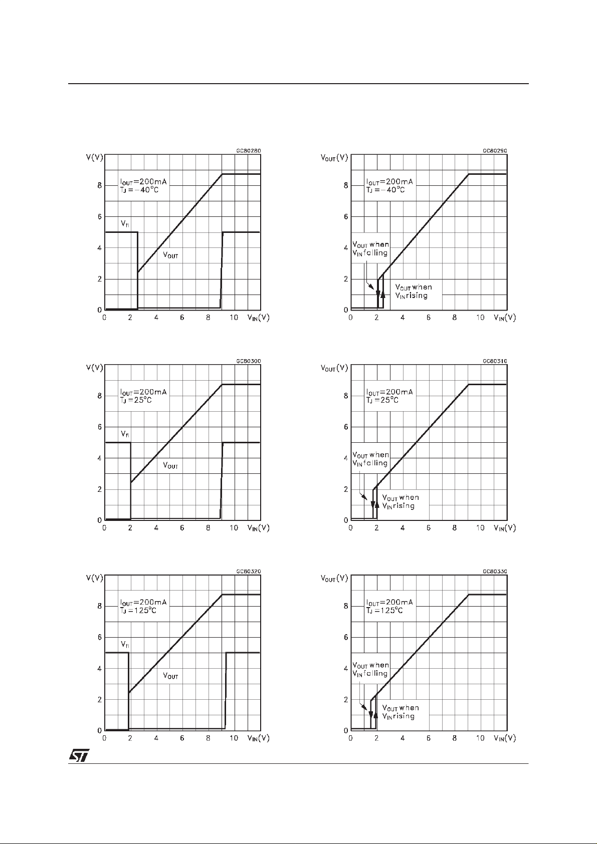
TYPICALPERFORMANCECHARACTERISTICS
Outputand Flag Voltage vs InputVoltage
Outputand Flag Voltage vs InputVoltage
(unless otherwisespecified T
OutputVoltage vs Input Voltage
OutputVoltage vs Input Voltage
=25oC, CIN=C
J
OUT
=1µF)
Outputand Flag Voltage vs InputVoltage
OutputVoltage vs Input Voltage
7/11
L4987 SERIES
APPLICATION HINT OF L4987CPT30
Howto usethe control flag
The flag produces a logic ”low” whenever the
output fall out out of regulation. An ”out of
regulationconditioncan result from:
1) Low Input Voltage (V
≤ V
IN
OUT+VDROP
)
2) CurentLimiting
3) Thermal Limiting
Figure 1 to 2 show the typical behaviour of the
output voltage and the control flag versus the
input voltageand thetemperatre.No hysteresis is
implemented;so the responseof V
OUT
and V
FLAG
are the same either when the VINramps up or
down.
The control flag is an open collector which
requires an externalpull-up resistor. This may be
connected to the regulator output (Figure 3) or
someother supply voltage(Figure 4).
Using the regulator output prevents an invalid
”high” on theflag which occurs if it is pulled up to
an external voltage while the regulator input
voltageis reducedbelow about 2V (Figue 5).
Concerning the pull-up resistor its value must be
properlychosen as suggestedbelow. When ”low”
as it is possible to see in figure 6 the control flag
voltageis:
V
FLAG(LOW)=VCE
= 0.5 = V
SUPPLY-RPULLxIFL
V
SUPPLY
while I
0.5V ≥ V
The minimum value of R
is chosen by design and, thus is known,
must be at maximum 10mA. Then
FL
SUPPLY-RPULL
x 10mA
, is, so, determined
PULL
by the following equation:
R
PULL(min)
≥ V
SUPPLY
Regarding the maximum value of R
0.5
-
mA
10
note that
PULL
its value depends of the type of logic used
(CMOS,TTL etc.), the transistor leackagecurrent
and the presence or not of a load on V
FLAG
.
The following example shows how to determine
the R
max in the case of CMOS logic, no
PULL
load and 10µA (for L4978 it is the maximum value
) of control flag leakage current.
of I
FH
Becaauseof CMOS logic:
2
≥
V
FLAG(HIGH)
3
V
SUPPLY
But:
V
FLAG(HIGH)=VSUPPLY-RPULLxIFH
2
≥
V
SUPPLY
3
so, the maximum value is determined by the
followingequation:
1
V
SUPPLY
R
PULL(MAX)
3
≤
10
A
Figure1:
8/11
Outputand Flag Voltage vs Input
Figure2:
FlagVoltage vs Input
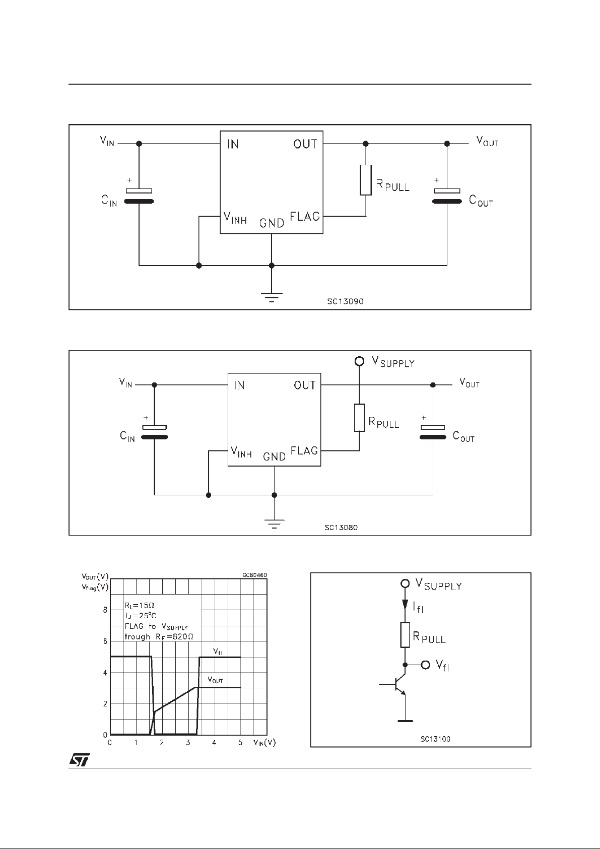
L4987 SERIES
Figure3:
TestCircuit
Figure4: Test Circuit
Figure5:
Outputand Flag Voltage vs Input
Figure6:
EquivalentOutput Circuit
9/11
L4987 SERIES
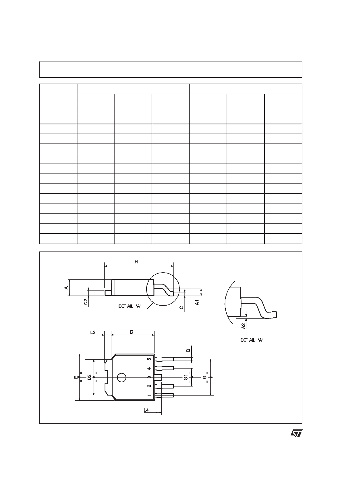
PPAK MECHANICAL DATA
DIM.
MIN. TYP. MAX. MIN. TYP. MAX.
A 2.2 2.4 0.086 0.094
A1 0.9 1.1 0.035 0.043
A2 0.03 0.23 0.001 0.009
B 0.4 0.6 0.015 0.023
B2 5.2 5.4 0.204 0.212
C 0.45 0.6 0.017 0.023
C2 0.48 0.6 0.019 0.023
D 6 6.2 0.236 0.244
E 6.4 6.6 0.252 0.260
G 4.9 5.25 0.193 0.206
G1 2.38 2.7 0.093 0.106
H 9.35 10.1 0.368 0.397
L2 0.8 1 0.031 0.039
L4 0.6 1 0.023 0.039
mm inch
10/11
0078180/B

L4987 SERIES
Information furnished is believed to be accurate and reliable. However, STMicroelectronics assumes no responsibility forthe consequences
of use of such information nor for any infringement of patents or other rights of third parties which may result from its use. No license is
granted by implication or otherwise under any patent or patent rights of STMicroelectronics. Specification mentioned in this publication are
subject to change without notice. This publication supersedes and replaces all informationpreviously supplied. STMicroelectronics products
are not authorized for use as critical components inlife support devices or systems without express written approval of STMicroelectronics.
The ST logo is a registered trademark of STMicroelectronics
1998 STMicroelectronics – Printed in Italy – All Rights Reserved
STMicroelectronics GROUP OF COMPANIES
Australia - Brazil - Canada - China -France - Germany - Italy - Japan - Korea - Malaysia - Malta - Mexico - Morocco - The Netherlands -
Singapore - Spain - Sweden - Switzerland - Taiwan - Thailand - UnitedKingdom - U.S.A.
http://www.st.com
.
11/11
 Loading...