

HALLEFFECT PICKUPIGNITION CONTROLLER
.DIRECT DRIVING OF THE EXTERNAL
POWERDARLINGTON
.
COIL CURRENT CHARGING ANGLE (dwell)
CONTROL
.
PROGRAMMECOILCURRENT PEAKLIMITATION
.PROGRAMMABLEDWELL RECOVERY TIME
WHEN 94 % NOMINAL CURRENT NOT
REACHED
.
RPMOUTPUT
.PERMANENTCONDUCTION PROTECTION
.
OVERVOLTAGE PROTECTION FOR EXTERNAL DARLINGTON
.
INTERNALSUPPLYZENER
.REVERSEBATTERY PROTECTION
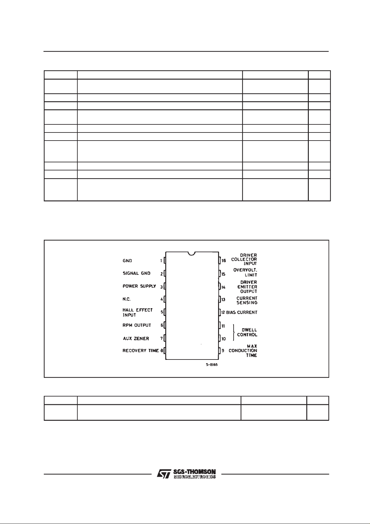
DES CRIPTION
TheL497is anintegratedelectronicignitioncontrollerforbreakerlessignitionsystemsusingHalleffect
sensors.
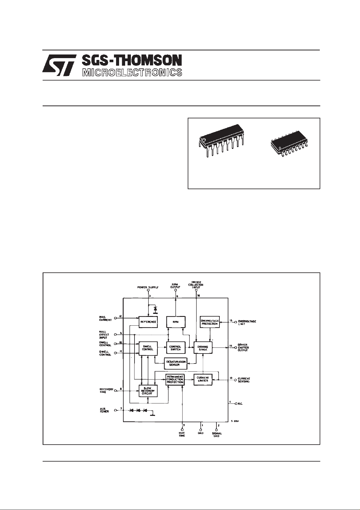
L4 97
DIP16 SO1 6
ORDERING NUMBERS : L497B(DIP16)
The device drives an NPN external darlington to
controlthecoilcurrentprovidingthe requiredstored
energywith lowdissipation.
A specialfeature of the L497 is the programmable
time for the recovery of the correctdwell ratio T
whenthecoil peakcurrentfailstoreach94 % ofthe
nominalvalue.Inthis wayonlyone sparkmayhave
anenergylessthan94 % ofthenominaloneduring
fast accelerationor coldstarts.
L497D1(SO16)
/T
d
BLOCK DI AGRAM
March 1998
1/11
L497
ABSOLUTE MAXIMUM RATINGS
Symbol Parameter Value Unit
200
800
3
300
600
15
35
1.2
0.65
V
V
I
V
I
V
T
j,Tstg
P
I
16
D.C. Supply current
3
Transient Supply Current (t
Supply Voltage Int. Limited to Vz
3
RPM Voltage 28 V
6
fall time constant = 100ms)
f
D.C. Driver Collector Current
Pulse ” ”(t <= 3ms)
Driver Collector Voltage 28 V
16
I
15
Auxiliary Zener Current 40 mA
7
D.C. Overvoltage Zener Current
Pulse ” ” t
Repetition Time > = 3ms
tr
ep
Reverse Battery Voltage if Application Circuit of Fig. 4 is used – 16 V
R
= 300µs,
fall
Junction and StorageTemperature Range – 55 to 150
Power Dissipation
tot
at T
=90°C for SO-16
aluminia
=90°C for DIP-16
T
amb
mA
mA
mA
mA
mA
mA
°C
W
W
PI N CONNECTIO N (top view)
THERMAL DATA
Symbol Parameter Value Unit
R
th j-amb
R
th j-alumin
(*) Thermal resist ance junction-aluminia w ith the device soldere d on the middle of an alum inia supporti ng substrate mesuring
15 x 20 ; 0.65 mm thicknes s.
Thermal Resistance Junction-ambient for DIP-16
(*)
Thermal Resistance Junction-alumina for SO-16
Max
Max
90
50
C/W
°
°C/W
2/11
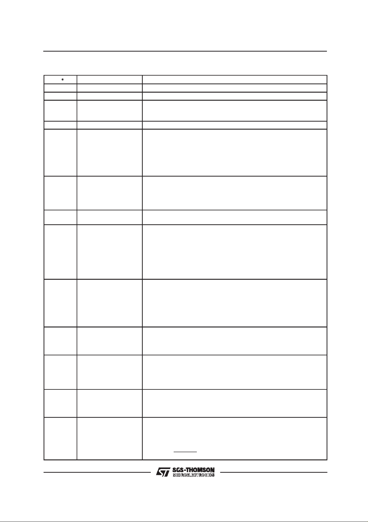
PIN FUNCTIONS (refer to fig. 4)
L497
N
°
Name Function
1 GND This pin must be connected to ground.
2 SIGNAL GND This pin must be connected to ground.
3 POWER SUPPLY Supply Voltage Input. An internal 7.5 V (typ) zener zener limits the voltage
at this pin. The external resistor R
limits the current through the zener for
5
high supply voltages.
4 N.C. This pin must be connected to ground or left open.
5 HALL-EFFECT INPUT Hall-effect Pickup Signal Input. This input is dwell control circuit output in
order to enable the current driving into the coil. The spark occurs at the
high-to-low transition of the hall-effectpickup signal.
Furthermore this input signal enables the slow recovery and permanent
conduction protection circuits. The input signal, supplied by the open
collector output stage of the Hall effect sensor, has a duty-cycle typically
about 70 %. V
is internally clamped to V3and ground by diodes
5
6 RPM OUTPUT Open collector output which is at a low level when current flows in the
ignition coil. For high voltages protection of this output, connection to the
pin 7 zener is recommended.
In this situation R
current if RPM module pad is accidentally connected to V
must limit the zener current, too, and R1limits pin 6
8
.
S
7 AUX. ZENER A 21 V (typ) General Purpose Zener. Its current must be limited by an
external resistor.
8 RECOVERY TIME A capacitor connected between this pin and ground sets the slope of the
dwell time variation as it rises from zero to the correct value. This occurs
after the detection of I
coll
94 % I
≤
, just before the low transition of the
nom
hall-effect signal pulse.
The duration of the slow recovery is given by :
= 12,9 R7C
t
src
where R
7
(ms)
src
is the biasing resistor at pin 12 (in KΩ) and C
is the delay
src
capacitor at pin 8 (inµF).
9 MAX CONDUCTION
TIME
A capacitor connected between this pin and ground determines the
intervention delay of the permanent conduction protection. After this delay
time the coil current is slowly reduced to zero.
Delay Time T
T
=16 CpR7(ms)
p
where R
is given by :
p
is the biasing resistor at pin 12 (in KΩ) and CPis the delay
7
capacitor at pin 9 (inµF).
10 DWELL CONTROL
TIMER
A capacitor C
HAll effect output is High and is discharged at the High to Low transition of
connected between this pin and ground is charged when the
T
the Hall effect signal.
The recommended value is 100 nF using a 62 KΩ resistor at pin 12.
11 DWELL CONTROL The average voltage on the capacitor CW connected between this pin and
ground depends on the motor speed and the voltage supply. The
comparison between V
dwell control. For the optimized operation of the device C
and VCTvoltage determines the timing for the
CW
=CW; the
T
recommended value is 100 nF using a 62 KΩ resistor at pin 12.
12 BIAS CURRENT A resistor connected between this pin and ground sets the internal current
used to drive the external capacitors of the dwell control
(pin 10 and 11) permanent conduction protection (pin 9) and slow recovery
time (pin 8). The recommended value is 62 KΩ.
13 CURRENT SENSING Connection for the Coil Current Limitation. The current is measured on the
sensing resitor R
and taken through the divider R10/R11. The current
S
limitation value is given by :
I
sens
= 0.32 ⋅
R
10
RS⋅ R
+ R
11
11
3/11
L497
PIN FUNCTIONS (continued)
N
°
14 DRIVER EMITTER
Name Function
Current Driver for the External Darlington. To ensure stability and precision
OUTPUT
of T
desatCc
and R9must be used. Recommended value for R9is 2 KΩ in
order not to change the open loop gain of the system.
may be added to Ccto obtain greater flexibility in various application
R
c
situations.
and Rcvalues ranges are 1 to 100 nF and 5 to 30 KΩ depending on the
C
c
external darlington type.
15 OVERVOLTAGE LIMIT The darlington is protected against overvoltage by means of an internal
zener available at this pin and connected to pin 14. The internal divider
defines the limitation value given by :
R
3/R2
22.5
16 DRIVER COLLECTOR
INPUT
V
ovp
=
+
R
3
The collector current of the internal driver which drives the external
darlington is supplied through this pin. Then the external resistor R
5.10
−3
R
22.5
+
2
the maximum current supplied to the base of the external darlington.
ELECTRICAL CHARACTERISTICS
= 14.4V, – 40 °C<Tj< 125 °C unless otherwise specified)
(V
S
Symbol Parameter Test Conditions Min. Typ. Max. Unit
V
I
V
V
V
Min Op. Voltage 3.5 V
3
Supply Current V3=6V
3
Voltage Supply 28 V
S
Supply Clamping Zener Voltage IZ3= 70 mA 6.8 7.5 8.2 V
Z3
Input Voltage Low Status
5
V
=4V
3
5
7
18 25
13
0.6 V
High Status 2.5
Input Current V5= LOW – 400 – 50
5
Darlington Driver Sat. Current I14=50mA
= 180 mA
I
14
Current Limit. Sensing Voltage VS= 6 to 16 V 260 320 370 mV
CWCharge Current VS= 5.3 to 16V
V
= 0.5V
11
– 11.0 – 9.3 – 7.8 µ
0.5
0.9
V
V
I
16–14
SENS
I
11C
T = 10 to 33ms
I
11D
CW Charge Current VS= 5.3 to 16V
= 0.5V
V
11
0.5 0.7 1.0
T = 10 to 33ms
I
11C/I11D
VS = 5.3 to 16V
= 0.5V
V
11
7.8 22.0
T = 10 to 33ms See Note 1
I
SRC
I
SENSE
T
SRC
V
Z15
T
Percentage of Output Current
Determining the Slow Recovery
Control Start (fig. 2), note 1
Duration of Altered Small Contr.
Ratio after SRC Function Start
(fig. 2)
External Darlington over V Prot.
Zener Voltage
Permanent Conduction Time V5= High
P
=1µF
C
SRC
=62K
R
7
I15=5mA
=2mA
I
15
=1µF
C
P
= 62KΩ
R
7
Ω
90 94 98.5 %
0.8 s
19
18
22.5
21.5
26
25
0.4 1.1 1.8 s
6
limits
mA
mA
V
A
µ
V
V
A
µA
V
V
4/11

ELECTRICAL CHARACTERISTICS (continued)
Symbol Parameter Test Conditions Min. Typ. Max. Unit
V
I
6 leak
V
V
6SAT
Z7
12
RPM Output Saturation Voltage I6= 18.5 mA
=25mA
I
6
RPM Output Leakage Current VS=20V 50
Auxiliary Zener Voltage I7=20mA 19 27 V
Reference Voltage 1.20 1.25 1.30 V
0.5
0.8
L497
V
V
A
µ
Notes : 1.
td/tdesaturation ratio is given by:
2.
I
sense=Icoil
whenthe external Darlingtonis in theactiveregion.
APP LICATION INFORMAT I ON
Figure1 : MainWaveforms.
td
T
1
=
1 + I
⁄ I
11C
11D
5/11

L497
DWELLANGLECONTROL
The dwell angle control circuit calculates the con-
ductiontimeD forthe outputtransistorinrelationto
the speed of rotation,to the supply voltage and to
the characteristicsof the coil.
On the negativeedgeof the Hall-effectinputsignal
thecapacitorC
currentl
11D
beginsdischargingwithaconstant
W
. Whenthesetpeakvalueof thecoilcurrent is reached,this capacitor charges with a constant currentI
11C
= 13.3 x I
, and the coil current
11D
is kept constantby desaturationofthe drivenstage
and the externaldarlington.
The capacitor C
starts charging on the posi-
T
tive.edgeof the Hall-effectinput signal with a constant current I
. The dwell angle, and conse-
10C
quentlythestartingpointof the coilcurrentconduction,isdecidedbythe comparisonbetweenV
.
V
11
10
and
A positivehysteresisis added to the dwell comparatorto avoidspuriouseffectsandC
israpidlydis-
T
charged on the negative edge of Hall-effects input
signal.
In thisway theaverage voltageon C
increasesif
W
the motor speeddecreasesand viceversa in order
t
d
tomaintainconstanttheratio
t
d
is kept constant(and not
T
atanymotorspeed.
T
D
= cost)to control
T
the power dissipationand to have sufficienttimeto
avoidlow energy sparksduringacceleration.
DESATURATIONTIMESIN STATIC
CONDITIONS
InstaticconditionsandifC
T=CW
asrecommended
andif thevaluesoftheapplicationcircuitoffig.4are
used.
t
d
=
T
1 + I
1
11C/I11D
DESATURATIONTIMESIN LOWAND HIGH
FREQUENCYOPERATION
Dueto theupperlimitofthevoltagerangeofpin11,
if the componentsof fig.4 are used, below 10 Hz
(300 RPM for a 4 cylinder engine) the OFF time
reachesitsmaximumvalue(about50 ms)andthen
the circuit graduallylosescontrolof the dwellangle
becauseD = T – 50ms.
Over200Hz(6000RPMfora 4cylinderengine)the
availabletimeforthe conductionislessthan3.5ms.
Iftheusedcoilis6 mH,6A,theOFFtimeisreduced
to zeroand the circuitlosesthe dwellanglecontrol.
TRANSIENTRESPONSE
The ignition system must deliver constant energy
evenduringtheconditionofaccelerationand decelerationofthemotorbelow80Hz/s.Theseconditions
can be simulatedby means of a signal gene-rator
with a linearlymodulatedfrequencybetween 1 Hz
and200 Hz (thiscorrespondsto a changebetween
30 and 6000 RPM for a 4cylindersengine).
CURRENT LIMIT
Thecurrentin thecoilismonitoredbymeasuringthe
currentflowing in the sensing resistor Rson
I
sense
theemitterof theexternaldarlington.I
sense
isgiven
by :
I
sens e=Icoi l+I14
WhenthevoltagedropacrossRsreachestheinternalcomparatorthresholdvaluethefeedbackloopis
activatedandI
keptconstant(fig.1)forcing the
sense
externaldarlingtonin the active region.In this condition:
I
sense=Icoil
WhenaprecisepeakcoilcurrentisrequiredRsmust
betrimmedor anauxiliaryresistordivider(R
10,R11
added:
Icpeak(A)=
0.320
RS)
⋅
R10
R11
+1
SLOWRECOVERYCONTROL (fig.2)
If I
hasnot reached 94 % of thenominalvalue
sense
justbeforethenegativeedgeoftheHall-effectinput
signal, the capacitor C
and CWare quickly dis-
src
chargedaslongasthepick-upsignalis”low”.Atthe
next positive transition of the input signal the load
currentstartsimmediately,producingthe maximum
achievable T
; then the voltage on C
desat
SRC
increaseslinearlyuntilthestandbyisreached.During
thisrecoverytimetheC
voltageis convertedinto
SRC
a current which, substratedfrom the chargingcurrentof thedwellcapacitor,producesaT
lation.This means thatthe T
untilitsvaluereaches,afteratimeT
decreasesslowly
desat
SRC
modu-
desat
,thenominal
7% value.
Thetime T
= 12.9R7 C
T
rsc
whereR
C
thecapacitorat pin 8 (in µF).
src
isgivenby:
SRC
(ms)
SRC
isthebiasingresistoratpin12(inKΩ)and
7
)
6/11

L497
Figure2 : SRC : I
HJ: Input signal
I
: Coil current
C
Failureand Time Dependenceof ActiveRegion.
coil
: Voltageon capacitor C
V
CM
DST: Percentageof imposed desaturation time.
SRC.
Figure3 : PermanentConductionProtection.
PERMANENTCONDUCTION PROTECTION
(fig.3)
The permanentconductionprotectioncircuit monitorstheinputperiod,chargingCPwitha costantcurrentwhenthe sensorsignalishigh anddischarging
it whenthesensorsignalis low.Ifthe inputremains
highfora timelongerthan T
thevoltageacrossC
P
reachesan internallyfixedvalueforcingtheslowdecrease of coil current to zero. A slow decrease is
necessaryto avoidundesiredsparks.When the input signal goes low again C
is swiftly discharged
P
and the currentcontrolloop operatesnormally.
Thedelaytime T
is givenby :
P
(sec) = 18 CPR
T
P
7
WhereR7isthebiasingresistoronpin12 (in K)and
Cp the delaycapacitorat pin 9 (in µF).
P
7/11

L497
OTHER AP PLI CAT I O N NOTES
DUM P PROTECTION
Loaddump protectionmust be implemented by an
externalzenerif this functionis necessary.In fig.4
protects the driver stage, the connection be-
DZ
2
tweenpin 6 and 7 protectsthe output transistor of
pin6.MoreoverDZ
protectsboththepowersupply
1
input(pin 3) and Hall-effectsensor.
ResistorR
isnecessaryto limitDZ1currentduring
4
loaddump.
OVERVOLTAGELIMITATION
The external darlingtoncollectorvoltage is sensed
bythe voltagedividerR
increasesrisingR
or decreasingR3.
2
Due to theactivecircuit used,an R
. Thevoltagelimitation
2,R3
oCo
seriesnet-
Figure4 : ApplicationCircuit.
work is mandatory for stabilityduring the high voltagecondition.
valuesdepend on the darlingtonused in the
R
oCo
application.
Moreover the resistor R
is suggested to limit the
13
overvoltage even when supply voltage is disconnectedduringthe highvoltagecondition.
REVERSEBATTERYPROTECTION
Duetothepresenceofexternalimpedanceatpin6,
3, 16, 15 L497 is protectedagainstreverse battery
voltage.
NEGATIVESPIKEPROTECTION
If correct operation is requestedalso during short
negativespikes,thediodeD
andcapacitorCsmust
S
beused.
8/11

DIP16PACKAGE MECHANICAL DATA
L497
DIM.
MIN. TYP. MAX. MIN. TYP. MAX.
a1 0.51 0.020
B 0.77 1.65 0.030 0.065
b 0.5 0.020
b1 0.25 0.010
D 20 0.787
E 8.5 0.335
e 2.54 0.100
e3 17.78 0.700
F 7.1 0.280
I 5.1 0.201
L 3.3 0.130
Z 1.27 0.050
mm inch
9/11

L497
SO16PACKAGEMECHANICAL DATA
DIM.
MIN. TYP. MAX. MIN. TYP. MAX.
A 1.75 0.069
a1 0.1 0.2 0.004 0.008
a2 1.6 0.063
b 0.35 0.46 0.014 0.018
b1 0.19 0.25 0.007 0.010
C 0.5 0.020
c1
D 9.8 10 0.386 0.394
E 5.8 6.2 0.228 0.244
e 1.27 0.050
e3 8.89 0.350
F 3.8 4.0 0.150 0.157
L 0.5 1.27 0.020 0.050
M 0.62 0.024
S
mm inch
45° (typ.)
8°(max.)
10/11

L497
Information furnished is believed to be accurate and reliable. However, SGS-THOMSON Microelectronics assumes no responsibility for
the consequences of use of such information nor for any infringement of patents or other rights of third parties which may result from its
use. No license is granted by implicationor otherwise under any patent or patent rights of SGS-THOMSON Microelectronics. Specification
mentioned in this publication are subject to change without notice. This publication supersedes and replaces all information previously
supplied. SGS-THOMSON Microelectronics products are not authorized for use as critical components in life support devices or systems
withoutexpress writtenapproval of SGS-THOMSON Microelectronics.
Australia - Brazil - Canada - China - France - Germany - Italy - Japan - Korea - Malaysia - Malta - Morocco - The Netherlands-
1998 SGS-THOMSON Microelectronics – Printedin Italy – AllRights Reserved
SGS-THOMSON Microelectronics GROUP OF COMPANIES
Singapore - Spain - Sweden - Switzerland - Taiwan - Thailand - United Kingdom - U.S.A.
11/11
 Loading...