

Datasheet L4973V3.3, L4973D5.1, L4973D3.3, L4973V5.1 Datasheet (SGS Thomson Microelectronics)
L4973V3.3 - L4973V5.1
3.5A STEP DOWN SWITCHING REGULATOR
UPTO3.5ASTE PDOWNCO NVERTER
OPERATING INPUT VOLTAGE FROM 8V TO
55V
3.3V AND 5.1V (±1%) FIXED OUTPUT, AND
ADJUSTABLEOUTPUTSFROM:
0V TO 50V (3.3V type)
5.1VTO 50V (5.1 type)
FREQUENCYADJUSTABLEUP TO300KHz
VOLTAGEFEED FORWARD
ZERO LOAD CURRENT OPERATION (min
1mA)
INTERNAL CURRENT LIMITING (PULSE BY
PULSEAND HICCUPMODE)
PRECISE 5.1V (1.5%) REFERENCE VOLT-
AGEEXTERNALLYAVAILABLE
INPUT/OUTPUT SYNCHRONIZATION FUNC-
TION
INHIBIT FOR ZERO CURRENT CONSUMP-
TION (100µA Typ.at V
PROTECTION AGAINST FEEDBACK DIS-
CONNECTION
THERMAL SHUTDOWN
OUTPUTOVERVOLTAGEPROTECTION
SOFTSTART FUNCTION
CC
= 24V)
L4973D3.3 - L4973D5.1
MULTIPOWERBCD TECHNOLOGY
POWERDIP(12+3+3) SO20(12+4+4)
ORDERING NUMBERS:
L4973V3.3 (Powerdip)
L4973D3.3 (SO20)
L4973V5.1 (Powerdip)
L4973D5.1 (SO20)
DESCRIPTION
The L4973 is a step down monolithic power
switching regulator delivering 3.5A at fixed voltages of 3.3V or 5.1V and using a simple external
divideroutput adjustable voltage up to 50V.
Realized in BCD mixed technology, the device
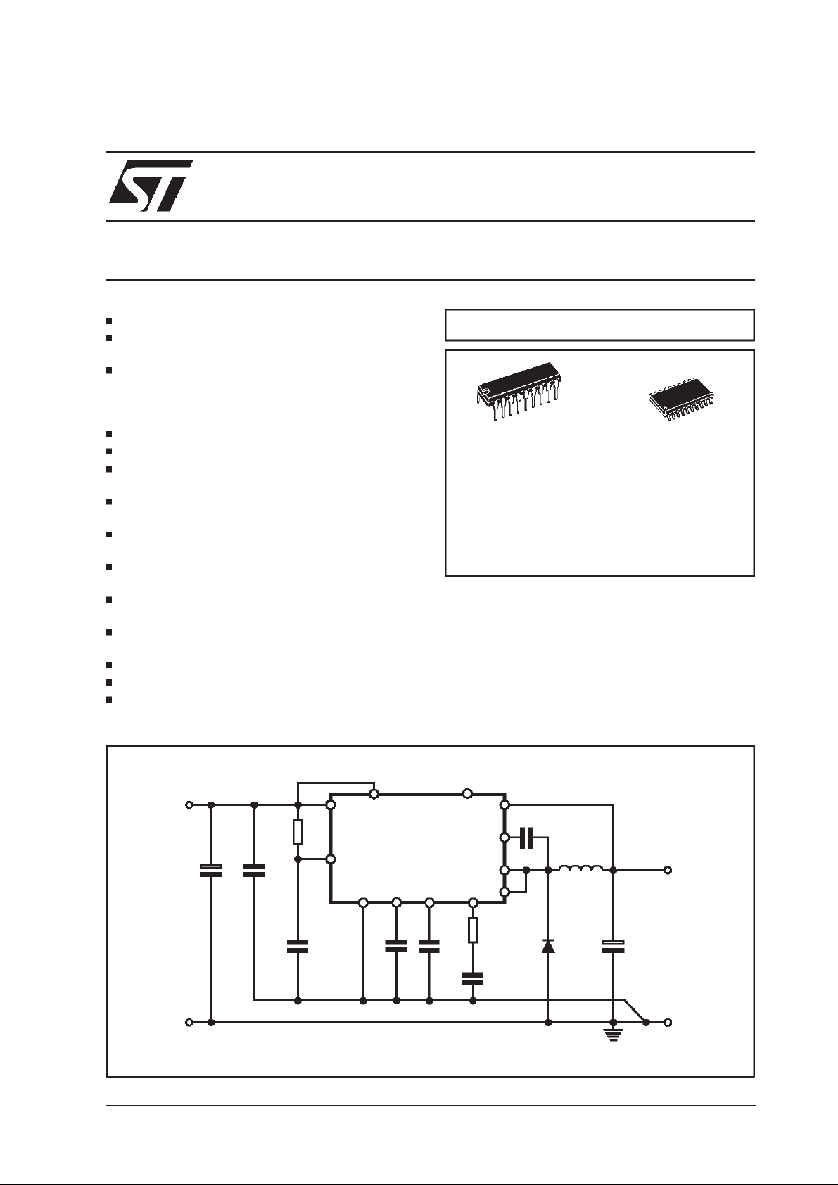
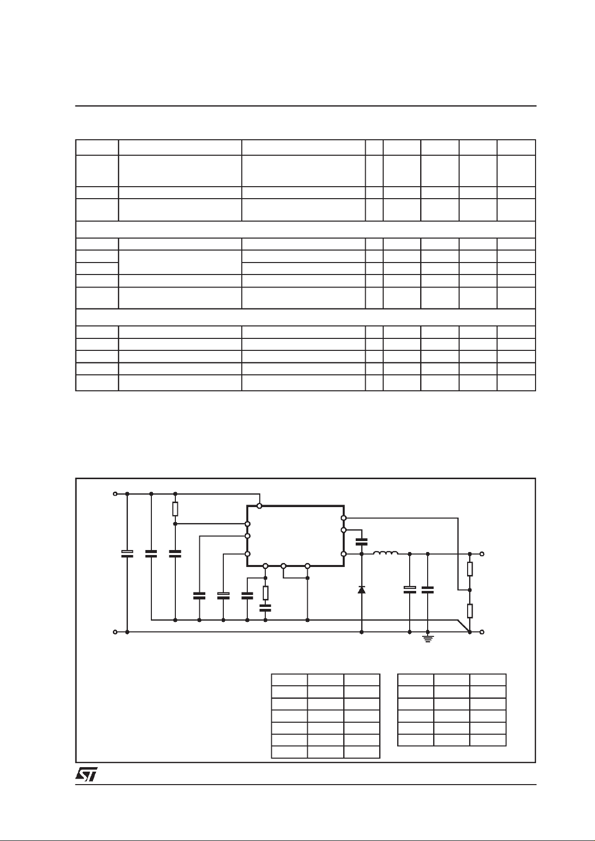
TYPICAL APPLICATIONCIRCUIT (POWERDIP)
VCC(8V to 55V)
798
R
OSC
L4973
16
April 2000
C
OSC
1
4,5,6,
13,14,15
C
IN
C2
17
C
SS
D97IN554A
10
11
12
3
2
R
C
C
COMP
COMP
BOOT
D1
L1
VO(3.3V or 5.1V)
C
OUT
1/16
L4973V3.3 - L4973V5.1 - L4973D3.3 - L4973D5.1
uses an internal power D-MOS transistor (with a
typicalRdson of 0.15ohm) to obtain very high efficiencyand very fast switching times.
Switching frequencyup to 300KHzare achievable
(the maximum power dissipation of the packages
mustbe observed).
A wide input voltage range between 8V to 55V
and output voltages regulated from 3.3V to 40V
coverthe majorityof thetoday applications.
Features of this new generation of DC-DC con-
PIN CONNECTIONS(Top view
OSC
OUT
OUT
GND
GND
GND
V
V
BOOT
1
2
3
4
5
6
7
CC
8
CC
9 INH
D94IN162A
POWERDIP (12+3+3)
17
16
15
14
13
12
11
10
)
SYNC18
SS
V5.1
GND
GND
GND
VFB
COMP
verterincludes pulse by pulse current limit, hiccup
mode for output short circuit protection, voltage
feed forward regulation, soft start, input/output
synchronization,protectionagainst feedback loop
disconnection, inhibit for zero current consumptionand thermal shutdown.
Packagesavailable are in plastic dual in line, DIP18 (12+3+3) for standard assembly, and SO20
(12+4+4)for SMD assembly.
OSC
OUT
OUT
GND
GND
GND
GND
V
CC
V
CC
BOOT INH
2
3
4
5
6
7
8
9
10
D94IN163A
20
19
18
17
16
15
14
13
12
11
SO20 (12+4+4)
SYNC1
SS
V5.1
GND
GND
GND
GND
VFB
COMP
BLOCKDIAGRAM
ZERO CURRENT
17(19)
SS
VFB
11(12)
5.1V
3.3V
12(13)
18(20)
Pin x = Powerdip
Pin (x) = S020
COMP
SYNC
2/16
INH
INHIBIT
+
E/A
-
V5.1
VREF
GOOD
SOFT
START
THERMAL
SHUTDOWN
-
PWM
+
OSCILLATOR
1(1) 2(2) 3(3)
5.1V
3.3V
(4,5,6,7,14,15,16,17)
INTERNAL
REFERENCE
HICCUP CURRENT
LIMITING
CURRENT
LIMITING
RSQ
4,5,6,13,14,15
INTERNAL
Q
V
SUPPLY
CC
DRIVER
5.1V
V
CC
8(9)7(8)16(18)10(11)
CBOOT
CHARGE
BOOT
9(10)
OUTOUTGNDOSC
D94IN161B
L4973V3 - L4973V5 - L4973D3- L4973D5
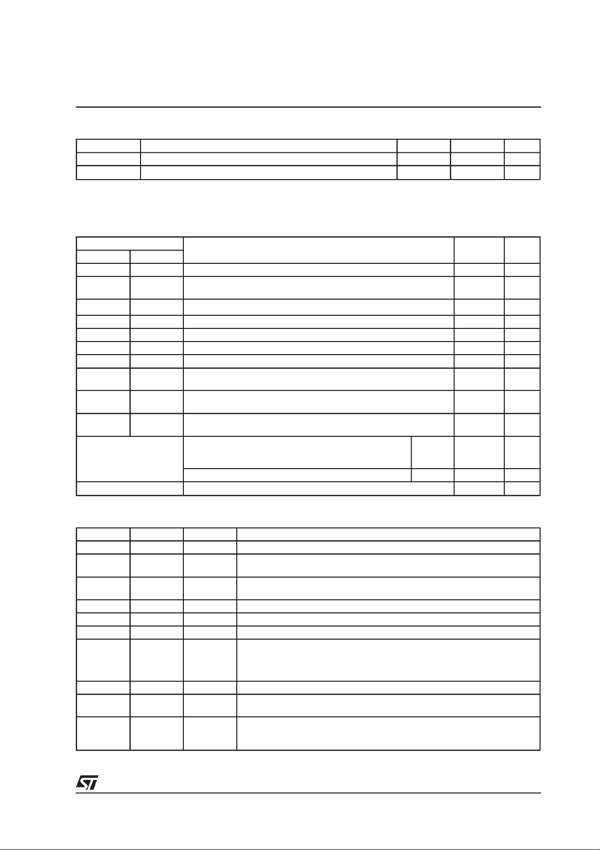
THERMALDATA
Symbol Parameter Powerdip SO20 Unit
R
th(j-pin)
R
th(j-amb)
(*) Package mounted on board.
ABSOLUTE MAXIMUM RATINGS
Thermal Resistance Junction to pin Max. 12 15 °C/W
Thermal Resistance to Ambient Max. 60 (*) 80 (*) °C/W
Symbol
DIP-18 S0-20
V
V
7,V8
2,V3
V9,V
V2,V
Input voltage 58 V
8
Output DC voltage
3
Parameter Value Unit
Output peak voltage at t = 0.1µs f=200KHz
V
I
2,I3
9-V8
V
V
V
V
9
11
17
12
I2,I
V10-V
V
10
V
12
Maximum output current int. limit.
3
8
Bootstrap voltage 70 V
Analogs input voltage (VCC= 24V) 12 V
14 V
V19 Analogs input voltage (VCC= 24V) 13 V
V
13
(VCC= 20V) 6
-0.3
V
18
V
20
(VCC= 20V) 5.5
-0.3
V
10
V
11
Inhibit Vcc
-0.3
P
T
J,TSTG
tot
Power dissipation a T
(T
=70°C no copper area)
amb
(T
=70°C 4cm copper area on PCB)
amb
Power dissipation a T
≤ 90°C
pins
=90°C SO20 4 W
pins
Junction and storage temperature -40 to 150 °C
DIP
12+3+3
1.3
PIN FUNCTIONS
Powerdip SO20 NAME DESCRIPTION
11 12 COMP E/A output to be used for frequency compensation
10 11 INH A logic signal (active high) disables the device (sleep mode operation).
9 10 BOOT A capacitor connected between thispin and the output allows to drive the
18 20 SYNC Input/Output synchronization.
7,8 8,9 Vcc Unregulated DCinput voltage
2,3 2,3 OUT Stepdown regulator output.
12 13 VFB Stepdown feedback input. Connecting the output directly to this pin results
16 18 V5.1 Reference voltage externally available.
4,5,6
13,14,15
4,5,6,7
14,15,16,17
GND Signal ground
1 1 OSC An external resistor connected between the unregulated input voltage and
If not used it must be connected to GND; if floating the deviceis disabled.
internal D-MOS.
in an output voltage of 3.3V for the L4973V3.3 and 5.1V. An external
resistive divider is required for higher outputvoltages. Foroutput voltage
less than 3.3V, seenote ** and Figure 32.
Pin 1 and a capacitor connected from Pin 1 to ground fixes the switching
frequency. (Line feed forward is automatically obtained)
-1
-5
V
V
V
V
V
V
V
V
5
W
W
2
W
3/16
L4973V3.3 - L4973V5.1 - L4973D3.3 - L4973D5.1
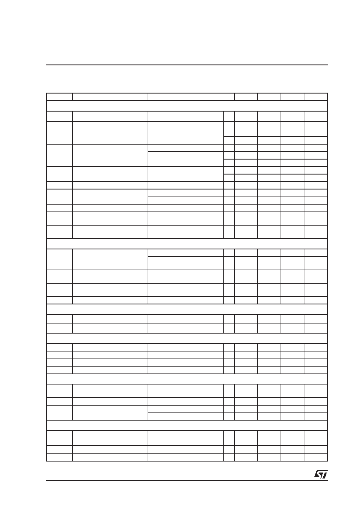
ELECTRICAL CHARACTERISTICS
R
OSC = 20K
Ω
; unless otherwisespecified)•= specificationsreferredto TJfrom0 to 125°C.
( Referto the test circuit,V
= 24V; Tj=25°C, COSC = 2.7nF;
CC
Symbol Parameter Test Conditions Min. Typ. Max. Unit
DYNAMIC CHARACTERISTICS
Input Voltage Range (*)
Output Voltage
L4973V5.1
Output Voltage
L4973V3.3
R
DSON
Maximum Limiting Current V
η Efficiency V
Switching Frequency
Supply Voltage Ripple
Rejection
Switching Frequency Stability
∆f
sw
vs, Supply Voltage
VO=V
I
= 1A 5.05 5.1 5.15 V
O
I
=0.5Ato3.5A 5.00 5.1 5.20 V
O
V
CC
I
= 1A 3.326 3.36 3.393 V
O
I
=0.5Ato3.5A 3.292 3.36 3.427 V
O
V
CC
VCC= 10.5V 0.15 0.22 Ω
I
=3.5A
O
CC = 8V to55V
O
V
O
V
i =VCC +2VRMS
VO=V
VCC= 8V to 55V 2 5 %
to 40V; I
REF
= 8V to 55V
=3.5A • 855V
O
•
4.95 5.1 5.25 V
= 8V to 40V • 3.26 3.36 3.46 V
•
•
4 4.5 5.5 A
0.35 Ω
= 5.1V; IO=3.5A 90 %
= 3.3V; IO=3.5A 85 %
•
90 100 110 KHz
60 dB
;IO=1A; f
ref
ripple
= 100Hz
REFERENCESECTION
Reference Voltage 5.025 5.1 5.175 V
I
Line Regulation I
Load Regulation V
= 0 to 20mA;
ref
V
= 8 to 55V
CC
= 0mA;
ref
V
= 8 to 55V
CC
= 0 to 5mA;
ref
V
= 0 to 20mA
CC
• 4.950 5.1 5.250 V
510mV
2
6
10
25
Short Circuit Current 30 65 100 mA
SOFT START
Soft Start Charge Current 30 45 60 µA
Soft Start Discharge Current 15 22 30 µA
mV
mV
INHIBIT
High Level Voltage
Low Level Voltage
I
source High Level V
I
source Low Level V
DC CHARACTERISTICS
Total Operating Quiescent
Current
Quiescent Current Duty Cycle= 0 2.7 4 mA
Total stand-by quiescent
current
ERROR AMPLIFIER
High Level Output Voltage 11.0 V
Low Level Output Voltage 0.65 V
Source Bias Current 1 2 3 µA
Source Output Current 200 300 600 µA
4/16
•
3.0 V
INH
INH
=3V
= 0.8V
•
•
10 16 50 µA
•
10 15 50 µA
0.8 V
Duty Cycle= 50% 4 6 mA
V
CC = 24V; V
V
CC = 55V; V
= 5V 100 200 µA
INH
= 5V 150 300 µA
INH
ELECTRICAL CHARACTERISTICS (continued)
Sink Output Current 200 300 µA
Supply Voltage Ripple
Rejection
VCOMP = VFB
C
=4.7µF 1-5mA load
REF
current
DC Open Loop Gain R
Transconductance I
L = ∞ 50 60 dB
= -0.1 to 0.1mA;
comp
V
=6V
comp
OSCILLATORSECTION
Ramp valley 0.78 0.85 0.92 V
Ramp peak V
CC = 8V 1.9 2.1 2.3 V
V
CC = 55V 9 9.6 10.2 V
Maximum Duty Cycle 95 97 %
Maximum Frequency Duty Cycle= 0%; R
13KΩ;C
OSC
SYNC FUNCTION
High Input Voltage VCC= 8V to55V 3.5 V
Low Input Voltage V
Slave Sink Current 0.15 0.25 0.45 mA
Master Output Amplitude I
Output Pulse Width no load, V
= 8V to55V 0.9 V
CC
= 3mA 4 4.5 V
source
L4973V3 - L4973V5 - L4973D3- L4973D5
60 80 dB
2.5 mS
=
OSC
= 820pF;
= 4.5V 0.20 0.35 µs
sync
500 KHz
(*) Pulse testingwith a low dutycycle.
(**) The maximum power dissipation of thepackage must be observed.
Figure1. EvaluationBoard Circuit
V
CC
C1 C2R2C7
C3 C4 C5
C1=1000µF/63V
C2=220nF/63V
C3=470nF
C4=1µF/50V
C5=220pF
C6=22nF
C7=2.7nF
C8=220nF/63V
C0=100µF/40V(C9,C10,C11)
C12=Optional (220nF)
L1=150µHK
R1=9.1K
R2=20K
D1=GI SB560
77310 - 40Turns - 0.9mm
OOLµ
7,8
1
17
16
(DIP18)
L4973
11
10
13,14,15
R1
C6
(V) R3(KΩ) R4(KΩ)
V
O
3.3
5.1
12
15
18
24
12
4,5,6
2,3
D97IN515B
L4973 V3.3
0
2.7
12
16
20
30
9
C8
D1
L1
3
x
C0
C12
V
R3
R4
O
L4973 V5.1
VO(V) R3(KΩ) R4(KΩ)
4.7
4.7
4.7
4.7
4.7
5.1
12
15
18
24
6.2
9.1
12
18
0
4.7
4.7
4.7
4.7
5/16

L4973V3.3 - L4973V5.1 - L4973D3.3 - L4973D5.1
TypicalPerformance (Using EvaluationBoard) fsw = 100kHz
Output Voltage
Figure1a:
Output
Ripple
3.3V 20mV 81.5(%) 3mV 6mV
5.1V 20mV 86.7(%) 3mV 6mV
12V 30mV 93.5 (%) 3mV (V
Efficiency
Line Regulator
I
= 3.5A VCC= 8 to 50V
o
CC =15 to 50V) 4mV
Load Regulator
VCC=35V IO= 1 to 3.5A
EvaluationBoard (Components Side)
Figure1b:
6/16
EvaluationBoard (SolderSide)

Figure1c: Application Circuit (see fig.1 part list)
V
CC
L4973V3 - L4973V5 - L4973D3- L4973D5
INH SYNC
7,8 10 18 9
1
17
C1 C2R2C7
C3 C4 C5
16
11
Figure1d: Application Circuit (see fig. 1 part list)
V
CC
7,8 10 18 9
1
17
C1 C2R2C7
16
11
L4973V5.1
4,5,6
13,14,15
R1
C6
D97IN665A
INH SYNC
L4973V3.3
4,5,6
13,14,15
C8
2,3
12
D1
L1
3
x
C0
Vo
C12
C8
12
2,3
L1
Vo
C3 C4 C5
Figure2:
QuiescentDrain Currentvs. Input
Voltage(0% DutyCycle)
Ibias
(mA)
5.0
Tamb=25°
0% DC
C
4.5
4.0
3.5
3.0
2.5
2.0
0 1020304050VCC(V)
200KHz-R2=22K
C7=1.2nF
D97IN633A
100KHz-R2=20K
C7=2.7nF
0Hz
R1
C6
D97IN664A
D1
3x
C0
C12
Figure3: Quiescent Drain Currentvs. Junction
Temperature
Ibias
(mA)
200KHz-R2=22K
4.0
100KHz-R2=20K
3.5
3.0
0% DC
VCC= 35V
0Hz
2.5
-50 0 50 100 Tj(°C)
D97IN634
C7=1.2nF
C7=2.7nF
7/16

L4973V3.3 - L4973V5.1 - L4973D3.3 - L4973D5.1
Figure4: Stand by Drain Currentvs. input
Voltage
Ibias
(µA)
V
=5V
inh
150
25°C
100
125°C
50
0 1020304050VCC(V)
D97IN635A
Figure6: ReferenceVoltage vs. Input Voltage
(Pin 16)
V
REF
(V)
5.15
Tj=25°
Pin 16
C
D97IN636A
Figure5: Reference Voltage vs. Junction
Temperature(Pin 16)
V
REF
D97IN637
(V)
Pin 16
5.15
Vcc=35V
5.1
5.05
5.0
-40 0 40 80 Tj(°C)-20 20 60 100
Figure7:
ReferenceVoltage vs. ReferenceInput
Current
V
REF
(V)
5.2
D97IN638
5.1
5.05
5.0
0 1020304050VCC(V)
Figure8:
Inhibit Current vs. Inhibit Voltage
(Pin 10)
Iinh
(µA)
Tj=0°C
Tj=125°C
100
50
0
Vcc=35V
Pin 10
D97IN651
Tj=25°C
Vcc=40V
5.1
5.0
4.9
0 1020304050I
Figure9:
V
Line Regulation (see fig. 1)
O
Vcc=10V
Tj=25°C
(V)
5.12
5.1
Tj=125°C
Tj=25°C
5.08
I
O
=1A
REF
D97IN639A
(mA)
8/16
-50
0 15 Vinh(V)105
5.06
0 1020304050VCC(V)

L4973V3 - L4973V5 - L4973D3- L4973D5
Figure10: LoadRegulation(seefig.1c)
VO
(V)
VCC= 35V
5.15
5.1
Tj=25°C
5.05
5.0
0123I
D97IN640
Tj=125°C
Figure12: LoadRegulation (see fig. 1d)
VO
(V)
3.35
3.34
3.33
3.32
3.31
VCC= 35V
Tj=125°C
Tj=25°C
D97IN661
(A)
O
Figure11: LineRegulation(seefig. 1d)
V
O
D97IN660A
(V)
3.35
3.34
3.33
Tj=125°C
Tj=25°C
3.32
=1A
I
3.31
3.3
0 1020304050VCC(V)
O
Figure13: Switching Frequency vs.R2 and C7
(fig. 1)
fsw
(KHz)
500
200
100
50
20
10
0.82nF
1.2nF
2.2nF
3.3nF
4.7nF
5.6nF
D97IN630
Tamb=25°C
3.3
0123I
Figure14:
SwitchingFrequencyvs. Input Voltage
fsw
(KHz)
Tamb=25°C
105
100
95
90
0 1020304050VCC(V)
D97IN631
(A)
O
5
0 20 40 60 80 R2(KΩ)
Figure15:
SwitchingFrequency vs. Junction
temperature(see fig. 1)
fsw
(KHz)
105
100
95
90
-50 0 50 100 Tj(°C)
D97IN632
9/16

L4973V3.3 - L4973V5.1 - L4973D3.3 - L4973D5.1
Figure16: DropoutVoltage Between pin 7,8 and
2,3
∆V
(V)
Tj=125°C
0.6
0.4
0.2
0
0123I
Figure18:
Efficiencyvs. OutputVoltage
Tj=0°C
D97IN643
Tj=25°C
(A)
O
(DiodeSTPS745D)
η
(%)
98
96
94
92
100KHz
200KHz
D97IN642
Figure17: Efficiencyvs. Output Voltage
(see fig.1)
η
(%)
98
96
100KHz
94
200KHz
92
90
88
86
0102030 V
IO=
3A
VCC= 50V
D97IN641
Figure19: Efficiencyvs. Output Current
( see fig.1c)
η
(%)
VO=5.1V
95
90
Vcc=12V
Vcc=24V
fsw= 100KHz
D97IN645
(V)40
O
90
IO=
88
3A
VCC= 35V
86
0 101520 VO(V)30525
Figure20:
Efficiencyvs. OutputCurrent
(see fig.1c)
η
(%)
Vcc=12V
90
Vcc=24V
85
Vcc=48V
80
75
0123I
VO= 5.1V
fsw= 200KHz
D97IN646
(A)
O
85
80
0123I
Figure21:
Efficiencyvs. Output Current
Vcc=48V
(see fig.1d)
η
(%)
VO= 3.3V
90
Vcc=12V
85
80
75
0123I
Vcc=24V
Vcc=48V
fsw= 100KHz
D97IN644
(A)
O
(A)
O
10/16

L4973V3 - L4973V5 - L4973D3 - L4973D5
Figure22: Efficiencyvs. Output Current
(seefig.1d)
η
(%)
90
Vcc=12V
VO=3.3V
fsw= 200KHz
85
Vcc=24V
80
Vcc=48V
75
70
0123I
D97IN662
(A)0.5 1.5 2.5 3.5
O
Figure24: Power dissipation vs. Output Voltage
(Deviceonly)
Pdiss
(W)
3.0
2.5
2.0
1.5
1.0
V
=
35V
CC
fsw= 100KHz
D97IN648
IO=3.5A
I
=3A
O
=2.5A
I
O
I
=2A
O
Figure23: Power dissipation vs.Input Voltage
(Deviceonly) (see fig.1c)
Pdiss
(W)
1.5
1.0
0.5
0
0 10 30 40 Vcc(V)20 50
I
O
=2.5A
I
O
=3A
IO=3.5A
I
=2A
O
D97IN647A
=
5.1V
V
O
fsw= 100KHz
Figure25: Pulse by Pulse Limiting Current vs.
Junction Temperature
Ilim
(A)
5.2
5
4.8
Vcc=35
4.6
D97IN652
0.5
0
0 5 15 20 VO(V)10 25 30
Figure26:
I
O
LoadTransient
(A)
3
2
1
T
2
200µs/DIV
1
T
VCC= 35V
f
= 100KHz
sw
I
=1A
O
D97IN649
V
O
(mV)
100
0
-100
4.4
4.2
-40 -20 60 80 Tj(°C)0 12020 40 100
Figure27:
V
CC
Line Transient
(V)
30
20
10
1
2
1ms/DIV
IO= 1A
= 100KHz
f
sw
D97IN650
V
O
(mV)
100
0
-100
11/16

L4973V3.3 - L4973V5.1 - L4973D3.3 - L4973D5.1
Figure28: SourceCurrent Rise and Fall Time,
pin 2, 3 (Seefig1)
Figure30:Soft Start Capacitor Selection vs. In-
ductorand V
Lomax
(µH)
fsw= 200KHz
150
100
CC max (ref. AN938)
D97IN654
Css=56nF
Css=68nF
Css=47nF
Figure29: Soft Start Capacitor Selectionvs.
Inductorand V
Lomax
(µH)
300
250
200
150
100
50
0
25 30 35 40 Vi(V)5045
fsw= 100KHz
CC max (ref. AN938)
D97IN653
Css=1µF
Css=820nF
Css=680nF
Css=470nF
Css=220nF
Css=100nF
Figure31: Open Loop Frequency and Phase of
Erroramplifier
GAIN
(dB)
50
0
-50
GAIN
D97IN663
Phase
0
45
50
0
15 20 25 30 Vi(V)4035 45 50
Figure32:
V
3.5A at V
CC
C1 C2R2C7
< 3.3V(see part list fig. 1)
O
C3C4C5
Css=33nF
Css=22nF
INH SYNC
7,8 10 18 9
1
17
L4973V3.3
R5
D97IN666A
4,5,6
13,14,15
11
R1
C6
-100
-150
-200
2,3
1216
2
10 10
V
1.5 2K 2K
2.5 7.5K 3.6K
C8
L1
D1
3
C0
3
4
10
10
PR5R3
1 3.6K 4.7K
2 4.7K 3.6K
3 5.1K 1K
Vo
x
R3
5
10
V
Phase
6
O
7
10
=3.36-1.74•
10
90
135
8
f(Hz)10
R
3
R
5
12/16

L4973V3 - L4973V5 - L4973D3 - L4973D5
Figure33: 12V to 3.3V High Performance Buck Converter(fsw= 200kHz)
INH SYNC
VCC
12V±5%
C1
560uF-25V
HFQ
Panasonic
L1 KoolMm 77120- 24 Turns-
D1 STPS1025
Figure34: SynchronizationExample
C2
220nF
R2
22k
C7
1.2nF
C3
33nF
C4
1uF
7,8 10 18 9
1
17
L4973V3.3
16
11
C5
220pF
0.9mm
R1
9k1
C6
22nF
D97IN668A
4,5,6
13,14,15
C8
220nF
2,3
12
L1
Vo=3.33V
Io=3.5A
D1
C9
470uF-25V
HFQ
Panasonic
η
(%)
92
90
88
86
84
82
80
0.0 0.5 1.0 1.5 2.0 2.5 3.0 3.5 Io(A)
V
CC2
Figure35:
V
CC
C1 C2R2C7
7,8
1
L4973 L4973
18 18
4,5,6
13,14,15
13,14,15
V
7,8
1
4,5,6
CC1
V
CC
Multioutputnot Isolated (Pin out referred to DIP12+3+3)
INH SYNC
7,8 10 18 9
1
17
16
C3 C4 C5
11
R1
C6
L4973
4,5,6
13,14,15
12
2,3
7,8
1
L4973 L4973
18 18
4,5,6
13,14,15
C8
D2
n2
L1
n1
D1
C9 C10
7,8
4,5,6
1
13,14,15
D97IN669
Vo2
Vo1
C11
VO2=V
O1
PO2< 20%P
n1+n
n
1
O1
2
D97IN667A
13/16

L4973V3.3 - L4973V5.1 - L4973D3.3 - L4973D5.1
DIM.
MIN. TYP. MAX. MIN. TYP. MAX.
a1 0.51 0.020
B 0.85 1.40 0.033 0.055
b 0.50 0.020
b1 0.38 0.50 0.015 0.020
D 24.80 0.976
E 8.80 0.346
e 2.54 0.100
e3 20.32 0.800
F 7.10 0.280
I 5.10 0.201
L 3.30 0.130
Z 2.54 0.100
mm inch
OUTLINE AND
MECHANICAL DATA
Powerdip 18
14/16

L4973V3 - L4973V5 - L4973D3 - L4973D5
DIM.
MIN. TYP. MAX. MIN. TYP. MAX.
A 2.35 2.65 0.093 0.104
A1 0.1 0.3 0.004 0.012
B 0.33 0.51 0.013 0.020
C 0.23 0.32 0.009
D 12.6 13 0.496 0.512
E 7.4 7.6 0.291 0.299
e 1.27 0.050
H 10 10.65 0.394 0.419
h 0.25 0.75 0.010 0.030
L 0.4 1.27 0.016 0.050
K0°(min.)8°(max.)
mm inch
0.013
OUTLINE AND
MECHANICAL DATA
SO20
B
e
D
1120
110
L
hx45°
A
K
A1
C
H
E
SO20MEC
15/16

L4973V3.3 - L4973V5.1 - L4973D3.3 - L4973D5.1
Information furnished is believed to be accurate and reliable. However, STMicroelectronics assumes no responsibility for the consequences
of use of such information nor for any infringement of patents or other rights of third parties which may result from its use. No license is
granted by implicationor otherwise under any patent or patent rights of STMicroelectronics. Specification mentioned in this publication are
subject to change without notice. This publication supersedes and replaces all information previously supplied. STMicroelectronics products
are not authorized for useas critical components in life support devices or systems without express written approval of STMicroelectronics.
The ST logo is aregistered trademark of STMicroelectronics
2000 STMicroelectronics– Printed in Italy – All Rights Reserved
STMicroelectronics GROUP OF COMPANIES
Australia- Brazil- China - Finland- France - Germany -Hong Kong - India - Italy- Japan - Malaysia - Malta - Morocco -
Singapore - Spain - Sweden- Switzerland- United Kingdom - U.S.A.
http://www.st.com
16/16
 Loading...