

L4963
1.5AOUTPUT LOAD CURRENT
5.1 TO 36V OUTPUTVOLTAGERANGE
DISCONTINUOUS VARIABLE FREQUENCY
MODE
PRECISE(+/–2%) ONCHIP REFERENCE
VERYHIGH EFFICIENCY
VERYFEW EXTERNAL COMPONENTS
NOFREQ. COMPENSATION REQUIRED
RESET AND POWER FAIL OUTPUT FOR MICROPROCESSOR
INTERNALCURRENT LIMITING
THERMALSHUTDOWN
DESCRIPTION
TheL4963isa monolithicpowerswitching regulator
delivering1.5Aat 5.1V.Theoutputvoltageisadjustable from 5.1V to 36V, working in discontinuous
variable frequency mode. Features of the device
include remote inhibit, internal current limiting and
thermal protection, reset and power fail outputs for
microprocessor.
L4963D
1.5ASWITCHING REGULATOR
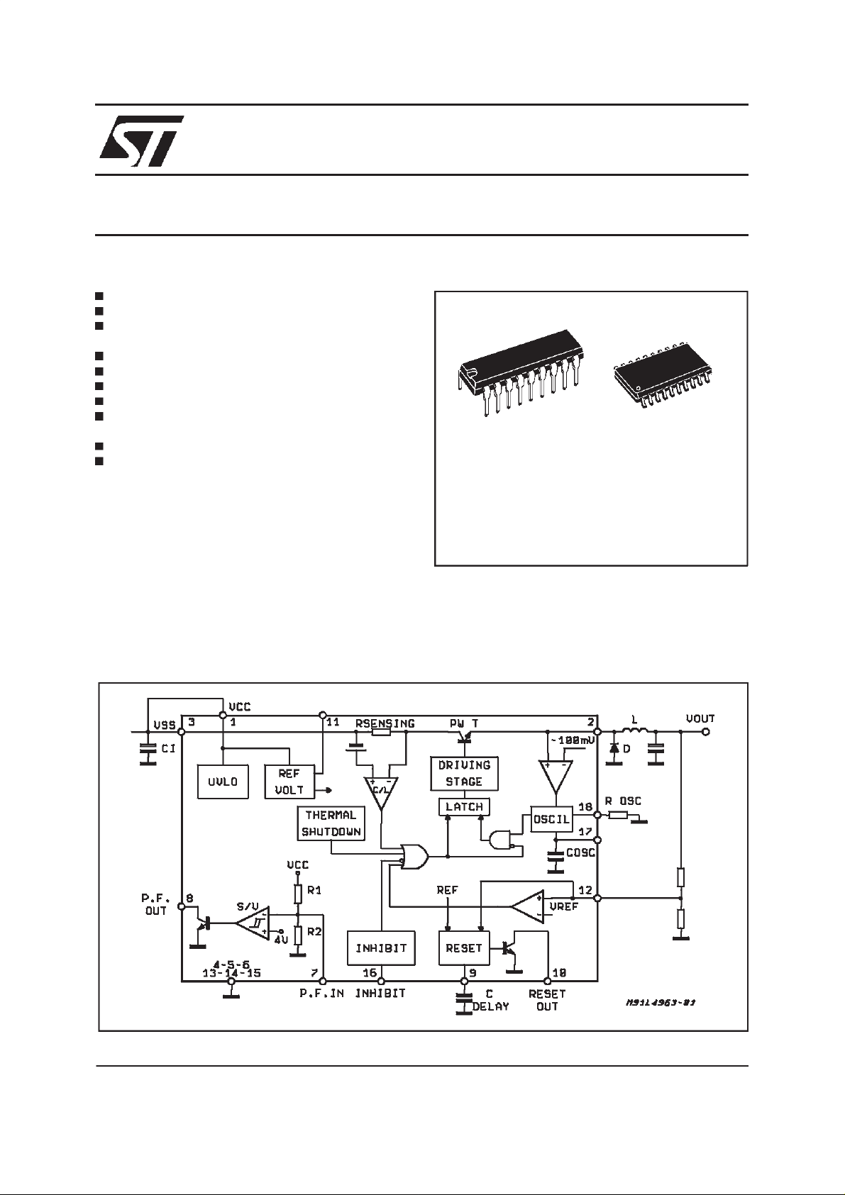
Powerdip12+3+3
ORDERING NUMBERS:
L4963W L4963D
TheL4963 is mounted in a 12+3+3lead Powerdip
(L4963) and SO20 large (L4963D) plastic packages and requiresvery few external components.
SO20
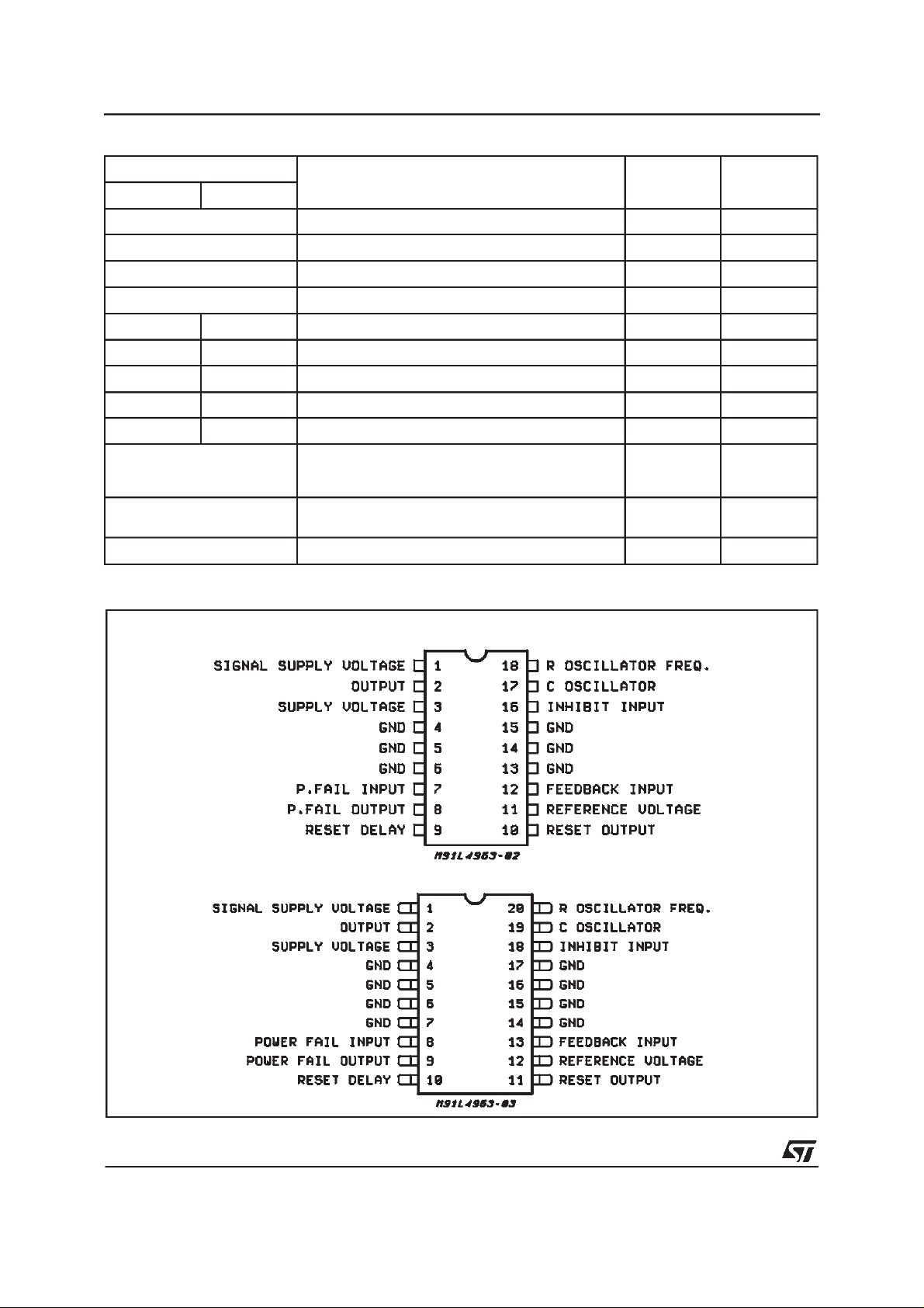
BLOCK DIAGRAM
June 2000
1/17
Thisis advanced information on a newproduct nowin development or underogin evaluation. Detailsaresubject tochange withoutnotice.
L4963 - L4963D
ABSOLUTEMAXIMUM RATINGS
Symbol
SO20 Powerdip
V
i
V
3–V2
V
2
V
2
V
8
V
9,V11
V
10
V
13,V18
V
19,V20
P
T
stg,Tj
P
tot
tot
V
7
V8,V
V
9
V12,V
V17,V
10
16
18
PIN CONNECTION(top view)
Parameter Value Unit
Input Voltage (pin 1 and pin 3 connectedtogheter)
47 V
Input to Output VoltageDifference 47 V
Negative OutputDC Voltage
Negative OutputPeak Voltage at t=0.2 µs, f=50kHz
–1 V
–5 V
Power Fail Input 25 V
Reset and PowerFail Output
V
i
Reset Delay Input 5.5 V
Feedback and Inhibit Inputs
7V
Oscillator Inputs 5.5 V
Total Power DissipationTpins ≤ 90°C (Power DIP)
=70°C no copper area on PCB)
(T
amb
=70°C, 4cm2copper area on PCB)
(T
amb
Storage & Junction Temperature
(Tamb= 70°C 6cm
2
copper area on PCB)
Total Power DissipationTpins ≤90°C (SO20L)
5
1.3
2
–40 to 150
1.45
4W
W
W
W
°C
W
Powerdip18
SO20
2/17
PIN FUNCTIONS
SO20L Power DIP Name Description
L4963 - L4963D
11
22
33
4, 5, 6, 7
14, 15, 16, 17
4, 5, 6
13, 14, 15
87
98
10 9
11 10
12 11
13 12
18 16
SIGNAL SUPPLYVOLTAGE Must be Connected to pin 3
OUTPUT Regulator output
SUPPLYVOLTAGE
Unregulated voltage input. An internal regulator
powers the internal logic.
GROUND Common ground terminal
Input of the power fail circuit. The threshold can be
POWER FAILINPUT
modified introducing an external voltagedivider
between the Supply Voltage and GND.
POWER FAILOUTPUT
RESET DELAY
RESET OUTPUT
Open collector power fail signal output. This output
is high when the supply voltage is safe.
A capacitor connected between this terminal and
ground determines the reset signaldelay time.
Open collector reset signal output. This output is
high when the output voltage value is correct.
REFERENCE VOLTAGE Reference voltage output.
Feedback terminal of the regulation loop.
FEEDBACK INPUT
The output is connected directly to this terminal for
5.1V operation; it is connected via a divider for
higher voltages.
INHIBIT INPUT
TTL level remote inhibit. A logic low level on this
input disables the device.
19 17
C OSCILLATOR
between this terminal and ground modifies the
maximum oscillator frequency.
Oscillator waveform. Acapacitor connected
20 18
R OSCILLATORFREQ.
A resistor connected between this terminal and
ground defines the maximum switching frequency.
THERMALDATA
Symbol Parameter SO20 Powerdip Unit
R
th j-pins
R
th j-amb
(*) See Fig. 28
Thermal Resistance Junction to Pins max.
Thermal Resistance Junction to Ambient (*) max. 85 80 °C/W
15 12 °C/W
3/17
L4963 - L4963D
CIRCUIT DESCRIPTION (Refer to Block Diagram)
The L4963 is a monolithicstepdownregulator providing 1.5A at 5.1V working in discontinuous variable frequency mode. In normal operation the
deviceresonatesata frequencydependingprimarily on the inductance value, the input and output
voltageand theloadcurrent.The maximumswitching howevercan be limitedby an internaloscillator,
which can be programmed by only one external
resistor.
The fondamental regulation loop consists of two
comparators, a precision 5.1V on-chip reference
anda drivelatch.Brieflytheoperationis as follows:
when the choke ends its dischargethe catch freewheeling recirculation filter diode begins to come
out of forward conduction so the outputvoltage of
the device approaches ground. When the output
voltagereaches–0.1V theinternalcomparatorsets
the latch and the power stage is turned on. Then
the inductor current rises linearly until the voltage
sensed at the feedback input reaches the 5.1V
reference.
The second comparator then resets the latch and
the output stage is turned off. The current in the
choke falls linearly until it is fully discharged, then
thecyclerepeats.Closingthe loop directlygivesan
output voltage of 5.1V.Higher output voltages are
obtained by inserting a voltage divider and this
method of control requires no frequencycompensation network. At output voltages greater than
5.1V the availableoutput current must be derated
due to the increased power dissipation of the device.
Outputoverload protection is provided by an internal current limiter.The load current is sensed by a
on-chip metal resistor connected to a comparator
whichresetsthe latch andturnsoffthe powerstage
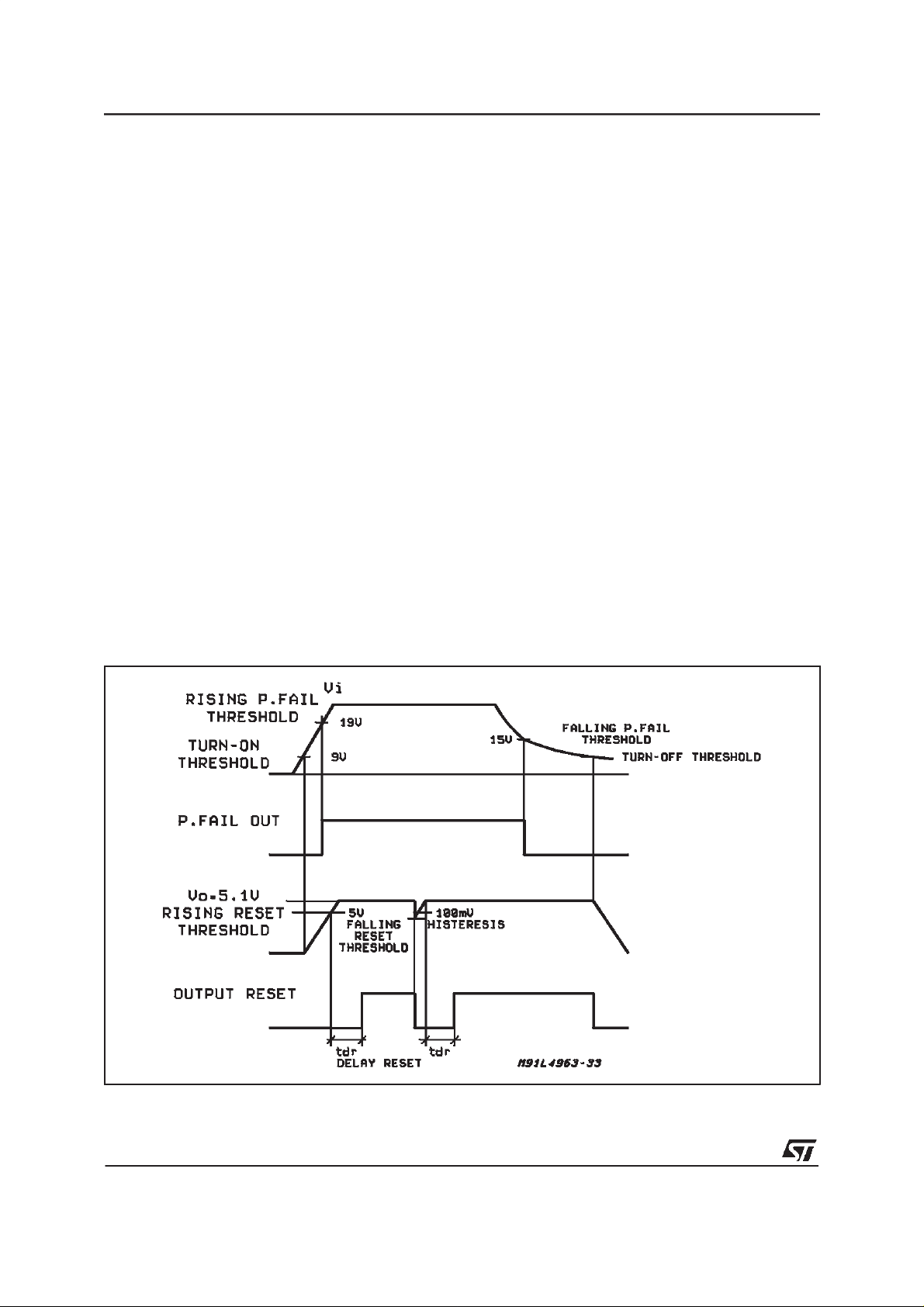
in overloadcondition. The reset circuits (see fig. 1)
generates an output high signal when the output
voltage value is correct. It has an open collector
output and the output signal delay time can be
programmed with an externalcapacitor. A powerfail circuit is also available and is used to monitor
the supply voltage. Its output goes high when the
supplyvoltagereachesapre-programmedtreshold
set by a voltage divider to its input from the supply
to ground.With the input left open the threshold is
approximately equal to 5.1V. The output of the
power fail is an open collector.
ATTLlevel inhibit isprovided for applicationssuch
as remote on/off control. This input is activated by
a low logic level and disables circuits operation.
The thermal overload circuit disables the device
when the junctiontemperatureis about150°Cand
has hysteresis to prevent unstable conditions.
Figure1:
Resetand Power Fail Function
4/17
L4963 - L4963D
ELECTRICAL CHARACTERISTIC (Referto the test circuit Vi=30VTj= 25°Cunlessotherwise specified)
Symbol Parameter Test Conditions Min. Typ. Max. Unit Fig.
DYNAMICCHARACTERISTICS
V
o
V
i
V
12
I
12
V
OS12
∆V
o
V
∆
o
V
d
I
2L
I
o
SVR
V
11
∆V
11
V
∆
11
η
T
sd
Output VoltageRange Vi= 46V Io= 0.5A
Input VoltageRange Vo=V
to 36V Io= 0.5A 9 46 V 2
ref
V
ref
36 V 2
Feedback Voltage Vi= 9 to 46V Io= 0.5A 5 5.1 5.2 V 2
Input Bias Current
i
=5V
V
17f
520µA3a
= 15V V12=6V
V
Input Offset Voltage 5 10 mV 3a
= 9 to 46V Vo=V
V
Line Regulation
Load Regulation
Dropout VoltageBetween
pin 3 and pin 2
Current Limiting
Maximum Operating Load
Current
Supply VoltageRipple
Rejection
Reference Voltage
Average Temperature
Coefficient of Ref. Volt.
V
Line Regulation Vi= 9 to 46V
ref
V
Line Regulation
ref
Efficiency I
i
Io= 0.5A
V
o=Vref
Io= 0.5 to 1.5A
I2=3A
= 20V
V
i
= 9 to 46V
V
i
V
o=Vref
= 9 to 46V Vo=V
V
i
= 2Vrms Vo=V
V
i
fripple = 100Hz Io= 1.5A
= 9 to 46V
V
i
O<I
= 0 to 125°C 0.4 mV/°C–
T
j
I
ref
= 46V R
V
i
= 1.5A Vo=V
o
Thermal Shutdown
Junction Temperature
to 28V
< 5mA
11
= 0 to 5mA
osc
ref
= 51KΩ
ref
ref
15 50 mV 2
15 45 mV 2
1.5 2 V 2
3.5 6.5 A 2
ref
1.5 A 2
50 56 dB 2
5 5.1 5.2 V 3a
10 20 mV 3a
65
69
715mV3a
65 75 % 2
145 150
C–
°
Hysteresis 30 °C–
DC CHARACTERISTICS
I
q
Quescent Drain Current
INHIBIT
V
16L
V
16H
I
16L
I
16L
Low Input Voltage Vi= 9 to 46V 0.3 0.8 V 2
High Input Voltage Vi= 9 to 46V
Input Current with Low
Input Voltage
Input Current with High
Input Voltage
V
i
= 0mA
I
o
V
16
V
16
= 46V
= 0.8V
=2V
V
16=V12
V
16=Vref
V12= 5.3V
= 0 14 20 mA 3a
11 16 mA 3a
2 5.5 V 2
50 100
A2
µ
10 20 µA2
5/17
L4963 - L4963D
ELECTRICAL CHARACTERISTIC
(Continued)
Symbol Parameter Test Conditions Min. Typ. Max. Unit Fig.
RESET
V
12
V
12
V
9D
V
9F
–I
9SO
I
9SI
I
10
V
10
Rising Threshold Voltage Vi= 9 to 46V
Falling Threshold Voltage Vi= 9 to 46V
Delay Rising Thereshold
Voltage
V
7
= OPEN
Delay Falling Thereshold
Voltage
Delay Source Current V9= 4.7V V12= 5.3V
V
–150
V
–150
4.3 4.5 4.7 V 3b
1 1.5 2 V 3b
70 110 140
V
ref
–100
V
ref
–200
Delay Sink Current V9= 4.7V V12= 4.7V 10 mA 3b
Output Leakage Current Vi= 46V V7= 8.5V
50
Output Saturation Volt. I10= 15mA; VI= 3 to 46V
V
ref
ref
ref
–50
V
ref
–250
0.4 V 3b
mV 3b
mV 3b
A3b
µ
A3b
µ
POWERFAIL
V
R
V
F
V
7
V
7
V
s
I
s
Rising Threshold Voltage Pin7 = open
Falling Threshold Voltage Pin7 = open 14.25 15 15.75 V 3c
Rising Threshold Voltage Vi= 20V
Falling Threshold Voltage Vi= 20V 3.325 3.5 3.675 V –
Output Saturation Volt. Ia=5mA
Output Leakage Current Vi= 46V 50 µA3c
17.5 19 20.5 V 3C
4.14 4.5 4.86 V –
0.4 V 3c
OSCILLATOR
f Oscillator Frequency RT= 51K
f
Oscillator Frequency
V
= 9 to 46V
I
= 0 to 125°C
T
j
= 51KΩ
R
T
Ω
46 60 79 kHz –
42 83 kHz –
6/17

Figure2: TestCircuit
Figure3: DC TestCircuit
Figure3a
L4963 - L4963D
Figure3b
7/17

L4963 - L4963D
Figure3c
Figure4: QuiescentDrain Current vs. Supply
Voltage(0% Duty Cycle)
Figure6:
QuiescentDrain Current vs. Junction
Temperature(0% Duty Cycle)
Figure 5:
QuiescentDrain Current vs. Supply
Voltage(100% Duty Cycle)
Figure7: QuiescentDrain Current vs. Junction
Temperature(100% Duty Cycle)
8/17

L4963 - L4963D
Figure8:
Figure10:
ReferenceVoltagevs. V
Line TransientResponse
i
Figure9: ReferenceVoltagevs. T
j
Figure11: LoadTransient
Figure12: SupplyVoltageRippleRejection vs.
Frequency
Figure13:
DropoutVoltageBetween pi3 and 2
vs. Current at pin2
9/17

L4963 - L4963D
Figure14: DropoutVoltageBetween pin3 and 2
vs. JunctionTemperature
Figure16: Power Dissipation (device only) vs. In-
put Voltage(Powerdip Package Only)
Figure 15: MaximumAllowablePowerDissipation
vs. Ambient Temperature(Powerdip
PackageOnly)
Figure17: Power Dissipation (device only) vs.
Output Voltage(PowerdipPackage
Only)
Figure18:
10/17
Voltageand Current Waveformat pin2
Figure19: Efficiencyvs. Output Current (Power-
dip Package Only)

L4963 - L4963D
Figure20:
Efficiencyvs. OutputVoltage(Power-
dip Package Only)
Figure21:
CurrentLimit vs. JunctionTempera-
tureV
= 30V
i
Figure 22: Current Limit vs. Input Voltage Figure 23: Oscillator Frequencyvs. R2 (seefig.26)
Figure24:
OscillatorFrequencyvs. Junction
Temperature
Figure25:
OscillatorFrequencyvs. Input Voltage
11/17

L4963 - L4963D
Figure26: EvaluationBoard Circuit
PARTLIST
CAPACITOR
C1 1000µF 50V EKR (*)
C2 2.2mF 16V
C3 1000µF 40V with low ESR
C4 1µF 50V film
RESISTOR
R1
1KΩ
Resistor Values for Standard Output Voltages
Diode:
V
O
12 4.7KΩ 6.2KΩ
15 4.7KΩ 9.1KW
18 4.7KΩ 12KW
24 4.7KΩ 18KW
BYW98
R6 R5
Core:L= 40µHMagnetics58121-A2MPP34Turns
R2
R3
R4
R5, R6
(*) Minimum 100µFifViisa preregulated offlineSMPS output or 1000µF if a 50Hztransformer plus rectifiers is used.
51KΩ
1KΩ
1KΩ
see table
0.9mm(20AWG)
12/17

L4963 - L4963D
Figure27: P.C.Board and ComponentLayoutof the Circuitof fig. 26 (Powerdip Package)(1:1 scale).
Figure28: ThermalCharacteristics
Figure29: Junction to Ambient ThermalResis-
tancevs. Area on BoardHeatsink
(SO20)
13/17

L4963 - L4963D
Figure30: AMinimal 5.1 Fixed Regulator— VeryFew Componentsare Required
Figure31: AMinimal Componentscount for V
=12V
O
14/17

L4963 - L4963D
DIM.
MIN. TYP. MAX. MIN. TYP. MAX.
a1 0.51 0.020
B 0.85 1.40 0.033 0.055
b 0.50 0.020
b1 0.38 0.50 0.015 0.020
D 24.80 0.976
E 8.80 0.346
e 2.54 0.100
e3 20.32 0.800
F 7.10 0.280
I 5.10 0.201
L 3.30 0.130
Z 2.54 0.100
mm inch
OUTLINE AND
MECHANICAL DATA
Powerdip 18
15/17

L4963 - L4963D
DIM.
MIN. TYP. MAX. MIN. TYP. MAX.
A 2.35 2.65 0.093 0.104
A1 0.1 0.3 0.004 0.012
B 0.33 0.51 0.013 0.020
C 0.23 0.32 0.009 0.013
D 12.6 13 0.496 0.512
E 7.4 7.6 0.291 0.299
e 1.27 0.050
H 10 10.65 0.394 0.419
h 0.25 0.75 0.010 0.030
L 0.4 1.27 0.016 0.050
K0°(min.)8°(max.)
mm inch
OUTLINE AND
MECHANICAL DATA
SO20
B
e
D
1120
110
L
hx45°
A
K
A1
C
H
E
SO20MEC
16/17

L4963 - L4963D
Information furnished is believed to be accurate and reliable. However, STMicroelectronics assumes no responsibility forthe consequences
ofuse of such information nor for any infringement of patents or otherrights of third parties which may result from its use. No license is granted
by implication or otherwise under any patent or patent rights of STMicroelectronics. Specification mentioned in this publication are subject to
change without notice. This publication supersedes and replaces all information previously supplied. STMicroelectronics products are not
authorized for use as criticalcomponents in life support devices or systems without express written approval of STMicroelectronics.
The ST logo is a registeredtrademark of STMicroelectronics
2000 STMicroelectronics – Printed in Italy– All Rights Reserved
STMicroelectronics GROUP OF COMPANIES
Australia - Brazil - China - Finland - France - Germany - Hong Kong - India - Italy - Japan - Malaysia - Malta - Morocco -
Singapore - Spain- Sweden - Switzerland - UnitedKingdom - U.S.A.
http://www.st.com
17/17
 Loading...