

L4955
5A ULDO LINEAR REGULATORS FAMILY
UP TO 5A OUTPUTCURRENT
2% PRECISEOUTPUT VOLTAGES
±
FASTTRANSIENTRESPONSE
0.75VTYP. DROP OUT VOLTAGEAT 5A
OPERATINGINPUT VOLTAGEFROM 4.5V
ADJUSTABLEVERSION:
= 1.26V
• V
O
• INHIBIT(I
POWERGOOD
•
PROGRAMMABLECURRENT LIMIT
•
= 120µA TYP.)
Q
• HEPTAWATT PACKAGE
FIXED VERSION:
• 3.3V,5.1V OUTPUTS
VERSAWATTPACKAGE
•
VERYLOW QUIESCENTCURRENT
SHORT CIRCUIT PROTECTION (Foldback
function)
THERMALSHUTDOWN
APPLICATIONS
PENTIUMANDPOWER PCSUPPLIES
POSTREGULATOR FOR SMPS
LOW COST SOLUTION FOR 5V TO 3.3V
CONVERSION
LOW COST BATTERYCHARGER
CONSTANT CURRENT REGULATOR
SUITABLE FOR APPLICATION WITH
STANDBYFEATURE
DESCRIPTION
The L4955 is a familyof monolithic ultra very low
drop linear regulators designed to supply the
most recent microprocessors.
TYPICALAPPLICATIONS
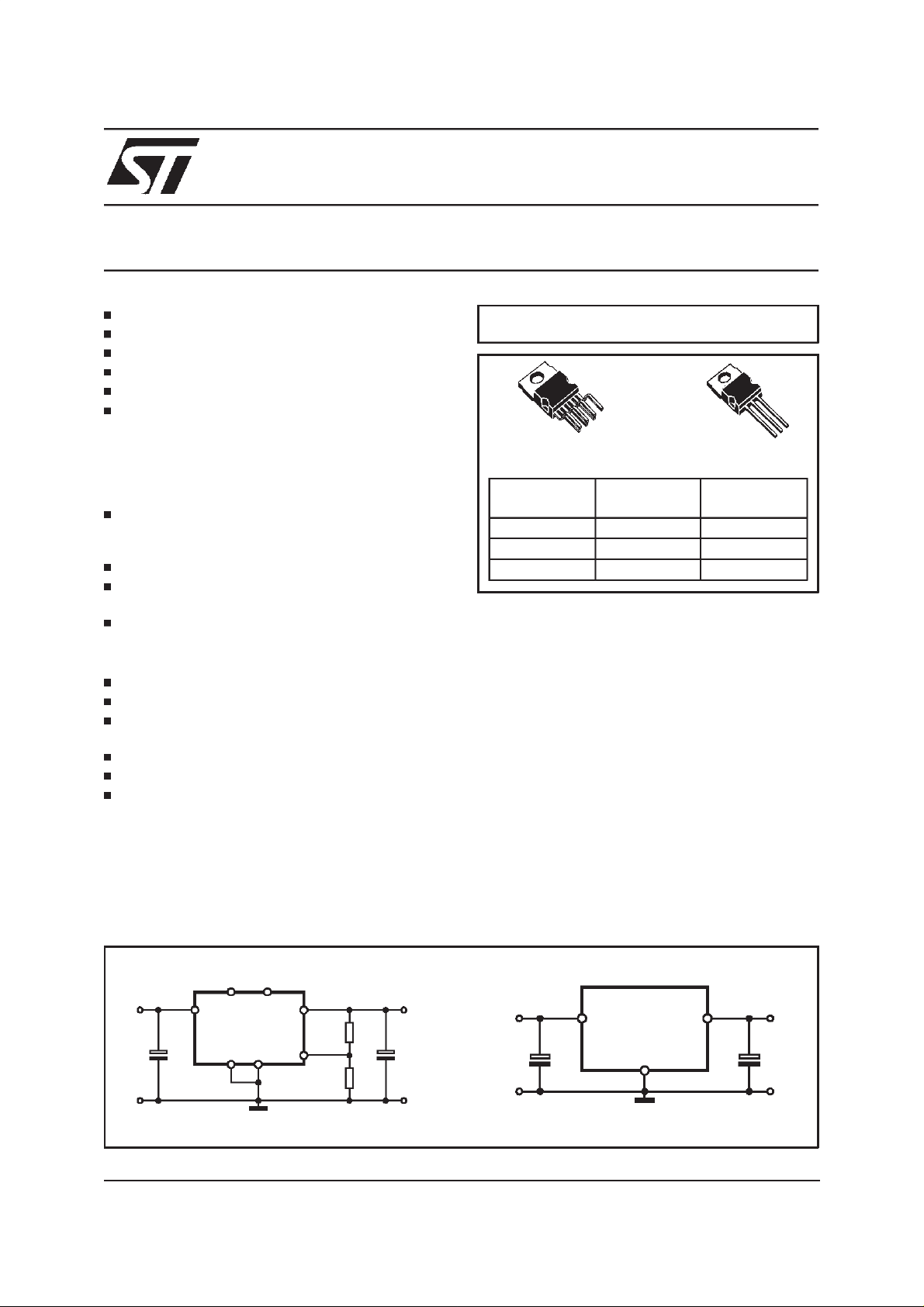
MULTIPOWER BCD TECHNOLOGY
HEPTAWATT VERSAWATT
ORDERING
NUMBERS
L4955 1.26V ADJ HEPTAWATT
L4955V3.3 3.3V VERSAWATT
L4955V5.1 5.1V VERSAWATT
OUTPUT
VOLTAGE
(TO-220)
PACKAGE
The dropout voltage is only 0.75V (Typ.) at 5A, directly dependenton the output current conditions.
Realized in BCDII technology, it has on board a
charge pump to properly drive an N-channel
powermos Transistorwith 150mΩof R
DSON
.
It operates from a 4.5V minimum supply, with a
very low quiescent current irrespective of the
load; a minimum of 22µF output capacitor is required for stability.
The on-chip trimming techniques improve the precisionof the availableoutputvoltages to±2%.
Ancillary functions like power good, inhibit with
low power consumption, programmable output
voltage and current limiting make the flexible
heptawatt version usable in applications where
power management, stand-by, features, post
regulation and adjustable current generators for
batterychargers are important.
V
IN
C1
February 1999
INH PG
1
CL GND
63
L4955
24
OUTIN
7
R1
ADJ
5
R2
D97IN589
C2
V
OUT
V
IN
C1
1
L4955VXXX
2
GND
3
D97IN590
OUTIN
C2
V
OUT
1/14
L4955
ABSOLUTE MAXIMUM RATINGS
Symbol Parameter Value Unit
V
IN
P
TOT
T
st,Ti
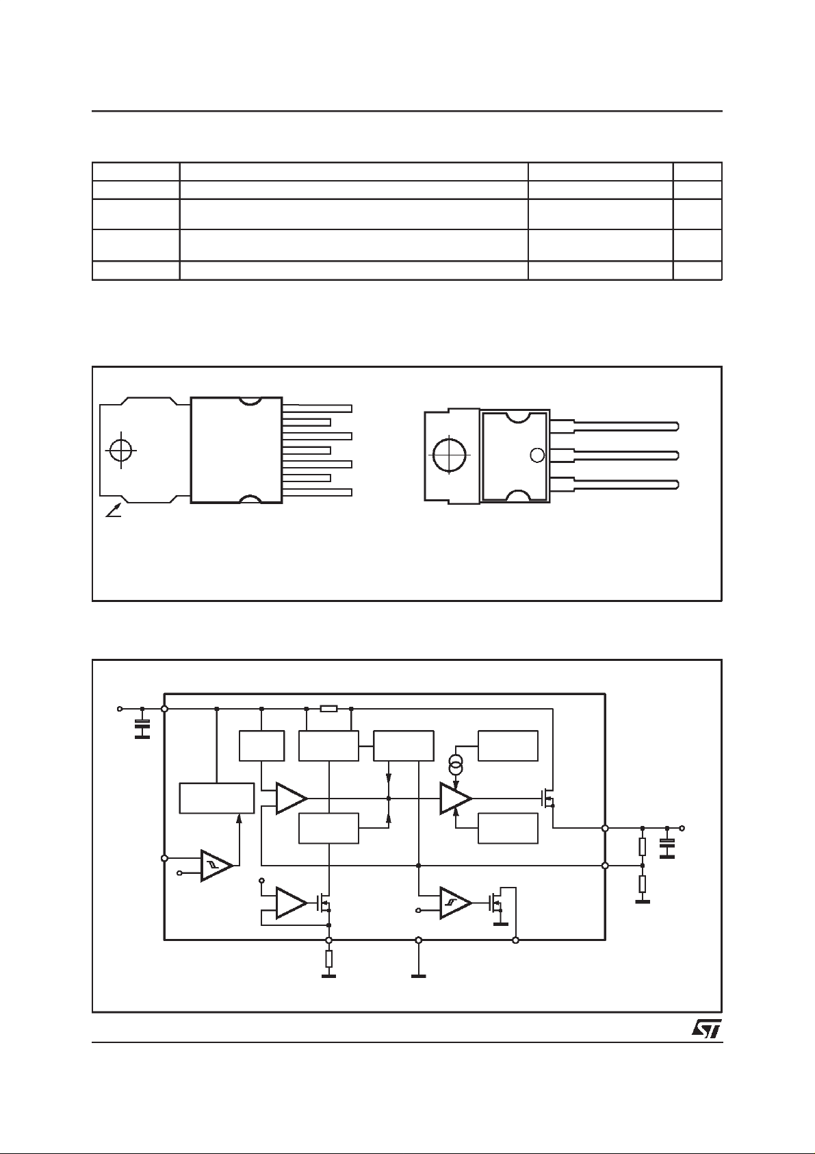
PIN CONNECTIONS (Top views)
tab connected to pin 4
Supply InputVoltage 24 V
ADJ and CL pins
PG and INH pins
Power Dissipation @ T
Power Dissipation @ T
amb
case
=50°C
=90°C
-0.3 to 4
0toV
2
15
IN
Storage Temperature -40 to +150 °C
7 OUT
6
5
4
3
2
1
D96IN367
PG
ADJ
GND
INH
CL
IN
3
1
D96IN369
V
V
W
W
OUT
GND
IN
HEPTAWATT
BLOCK DIAGRAM
10µF
IN
1(1)
REGULATOR
3
INH
1.26V
ACTIVE HIGH
PIN x =
PIN (x) = VERSAWATT
INHIBIT
V
IN
PRE
HEPTAWATT
V
REF
1.26V
V
REF
=
+
-
+
-
(1/4W, 1%)
VERSAWATT
(TO220)
FIXED
C.L.
E/A
PROGRAM.
C.L.
26
RCL
FOLDBACK
0.9V
REF
4(2)
+
-
GND PGCL
CHARGE
BUFFER
THERMAL
SHUTDOWN
PUMP
POWER
DMOS
150mΩ
D96IN366
OUT
7(3)
ADJ
5
R1 22µF
R2
V
OUT
2/14
PIN FUNCTIONS
HW VW Name Function
1 1 IN Unregulated input voltage; this pin must be bypassed with a capacitor larger than 10µF.
2 – CL A resistor connected between this pin and ground sets the programmable current limiting
value. When the programmable current limiting is not used the pin must be connected to GND.
3 – INH TTL-CMOS input. A logic high level on this input disables the device. An internal pull-down
insures full functionally even if the pin is open.
4 2 GND Ground.
5 – ADJ The output is connected directly to this terminal for 1.26V operation; it is connected to the
output through a resistivedivider for higher voltages.
6 – PG Opendrainoutput, this signal islow when the outputvoltage is lower than 90%,otherwise is high.
7 3 OUT Regulated output voltage. A minimum bypass capacitor of 22µF is requiredto insure stability.
L4955
THERMAL DATA
(HEPTAWATT& VERSAWATTpackages)
Symbol Parameter Value Unit
R
th j-case
R
th j-amb
Thermal ResistanceJunction-case Max. 2.5 °C/W
Thermal ResistanceJunction-ambient Max. 50 °C/W
Thermal Shutdown Typ. 150 °C
Thermal Hysteresis Typ. 20 °C
L4955 - ELECTRICAL CHARACTERISTICS (Tj=25°C, Vin= 12V, unless otherwise specified).
•
= Specificationsreferredto TJfrom0°Cto +125°C.
Symbol Parameter Test Condition Min. Typ. Max. Unit
V
IN
V
O
V
∆
∆V
V
O
I
O
I
Q
(1) Output voltage connected to ADJ.
OperatingSupply Voltage 4.5 22 V
Output Voltage (1) 0.1A< IO<5A; 4.5V< VIN<12V 1.235 1.26 1.285 V
4.5V < V
Line regulation (1) 4.5V < VIN<22V; IO= 10mA 2 10 mV
O
Load regulation (1) 0.1A < IO < 5A 2 10 mV
O
<12V; 0.1A< I
IN
Dropout Voltage IO=5A
V
4.5V
≥
IN
=2A • 0.55 0.75 V
I
O
<5A • 1.222 1.26 1.298 V
O
0.75 1.1 V
• 1.1 1.5 V
Current Limiting • 5.1 6.3 7.5 A
Short Circuit Current V
Programmable Current
Limiting
Quiescent Current 0.1A < IO<5A CL=0
=0V • 1.8 A
O
R
R
lim
lim
= 13kΩ
= 47k
Ω
•
•
2.55
0.7030.85
2
C
= 13k
L
2.7
Stand By Current INH = 5V 120 200
Inhibit Threshold Rising Edge
• 1.1 1.26 1.42 V
Inhibit Hysteresis 0.2 V
Inhibit Bias Sink Current INH = 5V or 0.8V 20 60
Power Good Threshold Rising Edge 0.9x V
Power Good Hysteresis
Power Good Saturation I
PG
= 4mA
Ripple Rejection f = 120Hz,I
V
=6V∆VIN=2V
IN
O
=5A
PP
• 0.2 V
•
60 75 dB
O
0.1 0.4 V
3.45
1.00
3
4
A
A
mA
mA
µ
µ
V
A
A
3/14
L4955
L4955V3.3 - ELECTRICAL CHARACTERISTICS
•
= Specificationsreferredto TJfrom0°Cto +125°C.
=25°C, Vin= 5V,unless otherwise specified)
(T
j
Symbol Parameter Test Condition Min. Typ. Max. Unit
V
V
∆
∆V
IN
O
V
I
O
I
Q
Operating Input Voltage 4.5 22 V
Output Voltage 4.75V< VIN<12V; 0.1A< IO< 5A 3.234 3.300 3.366 V
4.75V< V
Line regulation 4.5V < VIN<12V; IO= 10mA 2 10 mV
O
Load regulation 0.1A < IO < 5A 3 15 mV
O
<12V; 0.1A< I
IN
<5A • 3.201 3.300 3.399 V
O
Current Limiting • 5.1 6.3 7.5 A
Short Circuit Current V
=0V • 1.8 A
O
Quiescent Current 0.1A < IO<5A 2 3 mA
Ripple Rejection f = 120Hz,I
V
=6V∆VIN=2V
IN
O
=5A
PP
57 70 dB
L4955V5.1 - ELECTRICAL CHARACTERISTICS (Tj=25°C, Vin= 8V,unless otherwise specified)
•
= Specificationsreferredto TJfrom0°Cto +125°C.
Symbol Parameter Test Condition Min. Typ. Max. Unit
V
IN
V
O
V
D
Operating Input Voltage VO+V
D
Output Voltage 6.75V< VIN<15V; 0.1A< IO< 5A 5.000 5.100 5.200 V
6.75V < V
< 15V; 0.1A< I
IN
<5A • 4.950 5.100 5.250 V
O
Drop-out Voltage IO= 5A 0.75 1.1 V
22 V
• 1.1 1.5 V
=2A • 0.55 0.75 V
I
O
∆V
∆V
I
O
I
Q
Line regulation 6.5V < VIN<15V; IO= 10mA 2 10 mV
O
Load regulation 0.1A < IO < 5A 5 20 mV
O
Current Limiting • 5.1 6.3 7.5 A
Short Circuit Current V
=0V • 1.8 A
O
Quiescent Current 0.1A < IO<5A 2 3 mA
Ripple Rejection f = 120Hz,I
V
=8V∆VIN=2V
IN
O
=5A
PP
55 65 dB
4/14
L4955
L4955
Figure 1:
Ou tput C urrent [A ]
8
7
6
5
4
3
2
1
0
0 2.5 5 7.5 10 12.5 15 17.5 20 22.5
L4955 DC Operating Area
Current Lim itation
Rdson
limit
DC O perating A rea
Power D issipation Lim it
(Vin - Vout) [V]
Vin > 4.5V
Tj = 125°C
Tc = 25°C
Pdm ax = 40W
Tc = 70°C
Pdmax = 22W
Figure 3: LineRegulationvs. Junction
Temperature
5
4.5
4
3.5
3
2.5
2
1.5
1
Output Voltage Deviation [m V
0.5
0
-40 -20 0 20 40 60 80 100 120 140 160
Figure 5:
1.25
0.75
M in im u m V in - Vo u t Vo lta g e [V ]
0.25
DropoutVoltage
1
0.5
0
0123456
4.5V <Vin<22V
Iout=10mA
Tj[°C]
Tj = 125 °C
Tj= 25 °C
Tj= -40°C
Pulsed techniq ue has b een used
Iout [A]
Figure2:
OutputVoltage Stabilityvs. Junction
Temperature
Vout [V]
1.28
1.275
1.27
1.265
1.26
1.255
1.25
1.245
1.24
-40 0 40 80 120 160
Vin=12V
Iout=10m A
Tj [°C]
Figure4: Load Regulation
5
4
3
2
1
0
-1
-2
Output Voltage Deviation [m V ]
-3
-4
-5
012345
Figure6:
MaximumOutputCurrentvs.Junction
(Pulsed techn ique has been used)
Vin = 12V
Tj= 25 °C
Vo u t = V
Iou t [ A ]
ADJ
Temperatur ewithinternalcurrentlimiti ng
O utp ut C urre n t [A]
10
9
8
7
6
5
4
3
2
1
0
-40 -20 0 20 40 60 80 100 120 140 160
*Pulsed tecnique has been used
(Vin-Vout) > 2V
pin 2 = GND
Tj [°C]
5/14

L4955
Figure 7:
S ho rt-circuit Cu rrent [A]
3.5
3
2.5
2
1.5
1
0.5
0
-40 -20 0 2 0 40 60 80 100 12 0 140 160
*Pulsed tecnique has been used
Figure 9:
Iq [m A ]
5
4.5
4
3.5
3
2.5
2
1.5
1
0.5
0
Figure 11: Stand-byCurrent vs. Supply Voltage
Iq [u A ]
400
350
300
250
200
150
100
50
0
6/14
Short-circuitCurrent vs.Junction
Temperaturewith Programmable
Current Limiting
Rlim = 13 k
Rlim = 19 kΩ
Rlim = 47 kΩ
Tj [°C]
Ω
QuiescentCurrent vs. Supply voltage
(CL = 0V)
Io = 1 0 m A to 5 A
Tj= - 40°C
Tj=25°C
Tj=125°C
0 5 10 15 20 25
Vin[V]
with INH = LOGIC HIGH
Tj= 25°C
0 5 10 15 20 2 5
Vin [V]
L4955
Figure8:
Iq [m A]
2.6
2.4
2.2
2
1.8
1.6
1.4
1.2
1
0.8
0.6
0.4
-40-200 20406080100120140160
Figure10:
Iq [mA]
5
4.5
4
3.5
3
2.5
2
1.5
1
0.5
0
0 5 10 15 20 25
Figure12:
R ip p le R e je c tio n [d B ]
100
90
80
70
60
50
40
30
20
10
0
QuiescentCurrent vs.Temperature
(CL = 0V)
Vin=12V
Iout=10m A to 5A
Tj[°C]
QuiescentCurrent vs. Supply Voltage
with ProgrammableCurrent Limiting
Tj = 25°C
Rlim= 13k
Ω
Rlim = 47kΩ
Vin [V]
RippleRejection vs. Frequency
Vripple = 3V p-p V ripple = 0.5Vp-p
Cin = 22uF
Cout = 2 2uF
Vout = 1.26V
Vinmin = 4.5V
Io u t = 5 A
1k10 100 10k
Frequency [Hz]
100k

Figure 13: RippleRejection vs. OutputCurrent
L4955
Figure14:
L4955
PowerGood Function
R ipp le R e jec t io n [d B ]
100
90
Fripple=120Hz
Vripple=3Vp-p
80
70
60
50
Fripple=10kHz
Vripple= 0.5V p-p
Fripple=1kHz
V ripple= 0.5V p-p
40
30
20
10
Cin=22uF
Cout=22uF
Vout=1.26V
Vinmin=4.5V
0
012345
Iou t [A ]
Fripple=50kHz
Vripple=0.5Vp-p
Figure 15: InhibitFunction
V
INH
Vref = 1.26V
0.9 V
V
ADJ
PG
ADJ
Low
High
V
OUT=VADJ
hyst = 200mV
D96IN364B
(R1+R2)/R2
t
Low
t
hyst = 200mV
regulator
ON
regulator
OFF
regulator
ON
D96IN365A
t
t
7/14

L4955
LINE TRANSIENTRESPONSE
Figure 16.
Figure 17.
Figure 18.
Test condition
8/14
= 12V; ∆VIN= 1V; VO= 3.3V; IO=200mA; CIN=10µF (electrolyticcapacitor);
:V
IN
C
=22µF (electrolyticcapacitor);dV/dt = 0.1 V/µs; TJ=25°C
out

LOAD TRANSIENT RESPONSE
Figure 19.
Figure 21.
L4955
Figure20.
Test condition:
V
IN
= 5V, V
= 3.3V; Load Transient from 0.5A to 5A;
OUT
Figure 22: Loadtransient test circuit.
IN
L4955
C1,C2
470µ
F/25V
Panasonic
HFQ
2
CL GND
PG
6
43
INH
dI
out
dt
OUT
7
R4
ADJ
5
910
R5
560
C4 to
C9
100µ
F/10V
AVX TPS
6 each
D97IN546
A
⁄µs;TJ=25°C
= 20
C10 to
AVX
VOUT = 3.3VVIN = 5V 1
C15
1µF
X7R
6 each
9/14

L4955
L4955V3.3
Figure 23:
DCoperating area.
Output Current [A]
8
7
6
5
Curre nt L imitation
Power D issipation Limit
Rdson
4
3
2
1
0
limit
DC Operating Area
3 4.5 6 7.5 9 10.51213.51516.51819.52122.5
Vout = 3.3V
Tj = 125°C
Tc = 25°C
Pdmax=40W
Tc=70°C
Pdmax=22W
Input Voltage [V]
Figure 25: QuiescentCurrent vs. Temperature.
Iq [m A]
3
2.75
2.5
2.25
2
1.75
1.5
1.25
1
0.75
0.5
0.25
Vin=5V
Iout = 10mA to 5A
0
-40 -20 0 20 40 60 80 100 120 140 160
Tj[°C]
Figure24:
OutputVoltage Stability vs. Junction
Temperature.
Vout [V]
3.4
3.35
3.3
3.25
3.2
-40 0 40 80 120 160
Vin = 5V
Iou t = 10 mA
Tj [°C]
Figure26: Load Regulation
5
4
3
2
1
0
-1
-2
Output Voltage Deviation [mV]
-3
Vin=5V
Tj = 25 °C
-4
(Pulsed tec nique has been used)
-5
012345
Iout [A]
Figure 27:
Lineregulation vs. JunctionTemperature.
5
4.5
4
4.5V<Vin<12V
3.5
Iout = 10mA
3
2.5
2
1.5
Output Voltage Deviation [mV]
1
0.5
0
-40 -20 0 20 40 60 80 100 120 140 160
10/14
Tj [°C]
Figure28:
MaximumOutput Currentvs.Junction
Temperaturewith internalcurrentlimiting
O utp ut C urre n t [A]
10
9
8
7
6
5
4
3
2
1
0
-40 -20 0 20 40 60 80 100 120 140 160
*Pulsed tecnique has been used
(Vin-Vout) > 2V
pin 2 = GND
Tj [°C]

L4955V5.1
L4955
Figure 29:
Output C u rr ent [A ]
8
7
6
5
4
3
2
1
0
0 2.5 5 7.5 10 12.5 15 17.5
DCoperating area.
Curre nt Lim itation
Rdso n
limit
DC Operatin g Area
Pow er Dissipation Limit
(V in - Vout) [V ]
Vout = 5.1V
Tj = 125°C
Tc = 25°C
Pdmax = 40W
Tc = 70°C
Pdmax = 22W
Figure 31: QuiescentCurrent vs. Temperature.
Iq [mA]
3
2.75
2.5
2.25
2
1.75
1.5
1.25
1
0.75
0.25
Vin = 8 V
0.5
Iout = 10mA to 5A
0
-40 -20 0 20 40 60 80 100 120 140 160
Tj [°C]
Figure30:
OutputVoltage Stability vs. Junction
Temperature.
Vout [V]
5.2
Vin = 8V
5.15
5.1
5.05
5
4.95
4.9
Iout = 1 0mA
-40 0 40 80 120 1 60
Tj [°C]
Figure32: Load Regulation
10
8
6
4
2
0
-2
-4
Vin = 8V
Output Voltage Deviation [mV]
-6
Tj = 25 °C
(Pulse d tecn iqu e h as been used )
-8
-10
012345
Iout [A]
Figure 33:
Lineregulation vs. JunctionTemperature.
5
4.5
4
6.5V < Vin < 15V
Iout= 10mA
3.5
3
2.5
2
1.5
Output Voltage Deviation [mV]
1
0.5
0
-40 -20 0 20 40 60 80 100 120 140 160
Tj [°C]
Figure34:
Maximu mOutp utCur r entvs.Junction
Temperaturewith internalcurrentlimiting
O utp ut C urre n t [A]
10
9
8
7
6
5
4
3
2
1
0
-40 -20 0 20 40 60 80 100 120 140 160
*Pulsed tecnique has been used
(Vin-Vout) > 2V
pin 2 = GND
Tj [°C]
11/14

L4955
DIM.
MIN. TYP. MAX. MIN. TYP. MAX.
A 4.8 0.189
C 1.37 0.054
D 2.4 2.8 0.094 0.110
D1 1.2 1.35 0.047 0.053
E 0.35 0.55 0.014 0.022
E1 0.7 0.97 0.028 0.038
F 0.6 0.8 0.024 0.031
F1 0.9 0.035
G 2.34 2.54 2.74 0.095 0.100 0.105
G1 4.88 5.08 5.28 0.193 0.200 0.205
G2 7.42 7.62 7.82 0.295 0.300 0.307
H2 10.4
H3 10.05 10.4 0.396 0.409
L 16.7 16.9 17.1 0.657 0.668 0.673
L1 14.92
L2 21.24 21.54 21.84 0.386 0.848 0.860
L3 22.27 22.52 22.77 0.877 0.891 0.896
L4 1.29
L5 2.6 2.8 3 0.102 0.110 0.118
L6 15.1 15.5 15.8 0.594 0.610 0.622
L7 6 6.35 6.6 0.236 0.250
L9 0.2 0.008
M 2.55 2.8 3.05 0.100 0.110 0.120
M1 4.83 5.08 5.33 0.190 0.200 0.210
V4 40° (typ.)
Dia 3.65 3.85 0.144 0.152
mm inch
0.409
0.587
0.051
0.260
OUTLINE AND
MECHANICAL DATA
Heptawatt V
H3
L
VV
E
L1
M1
A
C
D
D1
L2
L5
L3
H1
Dia.
M
F
E1
E
GG1G2
H2
V4
L9
F
L7
L4
L6
F1H2
HEPTAMEC
12/14

L4955
DIM.
MIN. TYP. MAX. MIN. TYP. MAX.
A 4.40 4.60 0.173 0.181
C 1.23 1.32 0.048 0.051
D 2.40 2.72 0.094 0.107
E 0.49 0.70 0.019 0.027
F 0.61 0.88 0.024 0.034
F1 1.14 1.70 0.044 0.067
F2 1.14 1.70 0.044 0.067
G 4.95 5.15 0.194 0.203
G1 2.40 2.70 0.094 0.106
H2 10.0 10.4 0.393 0.409
L2 16.4 0.645
L4 13.0 14.0 0.511 0.551
L5 2.65 2.95 0.104
L6 15.25 15.75 0.600 0.620
L7 6.20 6.60 0.244 0.260
L9 3.50 3.93 0.137 0.154
M 2.6 0.102
Dia 3.75 3.85 0.147 0.151
mm inch
0.116
OUTLINE AND
MECHANICAL DATA
Versawatt (TO220)
M
TO220MEC
13/14

L4955
Informationfurnishedis believed to be accurat e and reliable. However, STMicroelectron icsassumes no responsi bilit yfor the consequences
of use of such information nor for any infringement of patents or otherrights of thirdparties which may result from its use. No license is
granted by implicationor otherwise underany patentor patent rightsof STMicroelectronics. Specification mentioned in thispublicationare
subjecttochange withoutnotice. This publicationsupersedes andreplaces all informationpreviouslysupplied.STMicroelectronicsproducts
are notauthorizedfor use as critical compo nentsinlife suppor tdevicesor syst em s without express writtenapprovalof STMicroelectronics.
The ST logoisa registeredtrademark of STMicroelectronics
1999 STMicroelectronics – Printedin Italy – AllRights Reserved
STMicroelectronics GROUP OF COMPANIES
Australia - Brazil- Canada - China - France - Germany - Italy - Japan - Korea - Malaysia - Malta - Mexico - Morocco - The Netherlands -
Singapore - Spain - Sweden - Switzerland- Taiwan - Thailand - United Kingdom - U.S.A.
http://www.st.com
14/14
 Loading...