

L4952
VOLTAGE REGULATOR FOR CAR RADIO APPLICATIONS
OPERATIONSUPPLY VOLTAGE9.5 TO 28V
PEAK SUPPLY OVERVOLTAGE PULSE UP
TO 52V (VS. GND)
FIXED OUTPUT VOLTAGE OF 8.6±0.2V
AND OUTPUT CURRENTUP TO 150mA
VERY LOW DROP OUTPUT STAGE WITH
LOW OUTPUTVOLTAGE DIAGNOSTIC
OUTPUT SHORT CIRCUIT AND THERMAL
OVERLOADPROTECTION
VERY LOW STANDBY CURRENT (DEVICE
DISABLED)
TWO INTERNAL OUTPUT VOLTAGE
SWITCHES WITH LOW DROPOUT FOR
AM/FM SWITCHING
DRIVER CIRCUIT FOR EXTERNAL HIGH
SIDE SWITCHWITH DROPMONITORING
ENABLE INPUT TO SWITCH ON THE DEVICE
ADDITIONAL 10V VERY LOW DROP REGULATOR TO SUPPLY THE VARICAP
DESCRIPTION
The L4952 is a monolithic voltage regulatorin an
advanced BCD60II process with high efficient pchannel transistor. This device is optimized for
Car Radio applications to obtain optimum performance and supply systemintegrationwith high
flexibilityand minimumperipheralcomponents.
June 2000
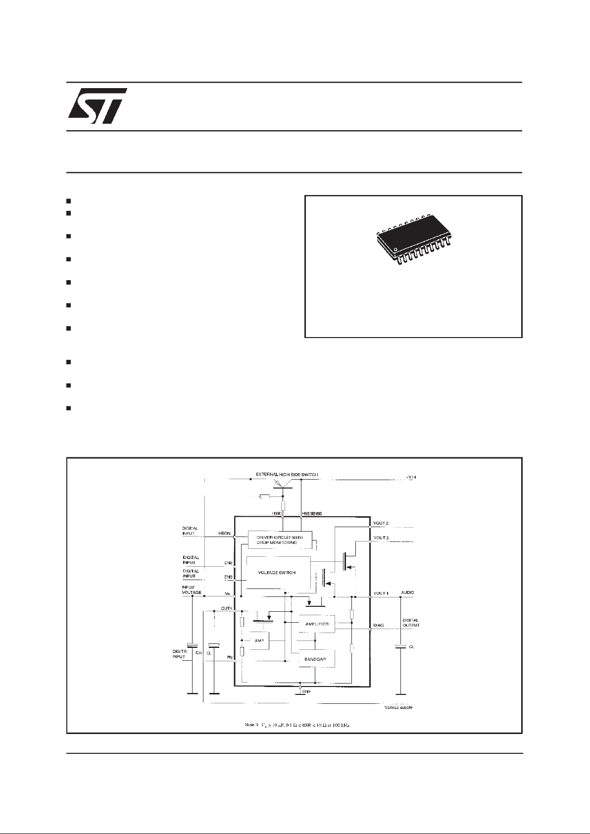
BLOCK DIAGRAM
SO20 (12+4+4)
ORDERING NUMBER:
L4952D
1/8
ABSOLUTE MAXIMUM RATINGS
Symbol Parameter Value Unit
V
s
DC supply voltage -2.2 .. +28 V
V
st
Transient operating supply voltage for t = 400ms -2.2 .. +52 V
V
o1,2,3,4
Output voltages -0.3 .. +12 V
V
EN
Input voltage of EN -0.3 .. +18 V
V
IND
Input voltage for EN2, EN3, HSON -18 .. +18 V
V
s-VIND
Max Voltage Difference between Vsand logic inputs EN2,
EN3,HSON
52 V
V
DIAG
Diagnostic output -0.3 .. +20 V
I
o1
Output current out1, out4 short circuit protected mA
I
o2,3
Output current out2,3 (Note 1) internally limited mA
I
oDIAG
Output current Diagnostic 10 mA
I
HSSD
Driver currentfor external pnp High side switch internally limited mA
T
J
Operating junction temperature -40 .. +150 °C
P
o
Power dissipation with on board heat sink 2cm
2
1W
V
ESD
ESD voltage capability ( MIL 883 C ) ±2000 V
Note: Current limiter of OUT1 will alsoprotectOUT2andOUT3aslongasOUT1is notreverse supplied.Output capacitors upto100µFbetween
OUT and GND will not harm this protection.
THERMAL DATA
Symbol Parameter Value Unit
R
th j-amb
Thermal ResistanceJunction to Ambient with on board heatsink
2cm
2
60 °C/W
T
JSD
Thermal shutdownjunction temperature >150 °C
OUT1
OUT3
EN3
GND
GND
GND
GND
EN2
OUT2 OUT4
DIAG
GND
GND
GND
GND
HSSD
HSSS
HSON1
3
2
4
5
6
7
8
9
18
17
16
15
14
12
13
11
19
10
20
V
S
EN
D95AU401A
PIN CONNECTION
L4952
2/8
FUNCTIONAL DESCRIPTION
The L4952 is a monolithic voltage regulator with
an output voltage of typically 8.6V and a maximum output current of 150mA. It ’s a device for
audio applicationsin carradios.
The device contain a precision Bandgap reference, a output amplifier with overcurrent protection, two voltage switches, a driver for an external
pnp switch, a discharge circuitry for theft detection and a overtemperatureprotection.
For automatic PCB assembly the package is
SO12+4+4.To use the maximalcurrent of 150mA
a small copper area of 2cm
2
as heat sink on
board (Rth=60K/W)is necessary.
The device has a very low quiescent current in
standby mode. If the digital Input EN is Low the
device is switched off (stand by mode) and if EN
ELECTRICALCHARACTERISTICS
(V
s
= 14V; TJ=25°Cunless otherwise specified)
Symbol Parameter Test Condition Min. Typ. Max. Unit
I
s
VsQuiescent current no Load 1.6 5 mA
I
ssb
Vsstandby current EN = 0V 0 20 µA
V
INLEN
Low Voltage EN -0.3 0.5 V
V
INHEN
High Voltage EN VS= 18V 3.5 18 V
V
IN L EN2,3
EN2, EN3, Low Voltage -18 1.05 V
V
IN H EN2,3
EN2, EN3, High Voltage VS= 18V 1.45 18 V
V
IN LHSON
HSON Low Voltage -18 1.0 V
V
IN H HSON
HSON High Voltage VS= 18V 2.0 18 V
I
INH
Current EN2, EN3, HSON VIn=5V 30 70 µA
I
INL
Current EN2, EN3, HSON VIn= 0V -10 10
µ
A
I
IN ON/OFF
Current High EN VIn= 5V -10 100 200 µA
Voltage Regulator (OUT 1)
V
o1
Output voltage no load 8.4 8.6 8.8 V
V
DP1
Dropout voltage Vs= 8.4V, V
DP1=Vs-Vout1
Io1= 0.15A, I
02,3
= 0mA 0.16 0.6 V
I
o1
= 0.1A, I
02,3
= 0mA 0.11 0.4 V
I
o1
= 0.05A, I
02,3
= 0mA 0.06 0.2 V
SVRR Supply Voltage ripple rejection f = 100Hz, C = 10µF ESR = 5Ω 60 70 dB
V
oLo
Load regulation 10mA < Io< 150 mA 30 60 mV
I
oLim1
Current limits V
OUT
= 8V 150 300 800 mA
Voltage Regulator (OUT 4)
V
o4
Output voltage no load 9.5 10.0 10.5 V
V
DP4
Dropout voltage I = 3mA Vs= 8.6V 0.14 0.3 V
I = 1.5mA V
s
= 8.6V 0.075 0.15 V
SVRR Supply Voltage ripple rejection f = 100Hz C = 10µF ESR = 5
Ω
30 60 dB
V
o4Lo
Load regulation 0.5mA < I < 3 mA 100 mV
I
o4Lim
Current limits V
OUT
=8V 8 60 mA
Diagnostic Output
V
LDIAG
Output Diagnostic Low voltage R
DIAG
to 5 V = 10K
Ω
0.4 V
∆V
out
Output voltage drop before
diagnostic activation
VS>6VIO1= 100mA
I
O2=IO3
= 0mA
30 200 mV
Voltage Switches Vout2/3
V
DP2
Dropout V
out2
Io2= 50mA, En2= H 0.25 0.5 V
I
o2
= 25mA, En2= H 0.125 0.25 V
V
DP3
Dropout V
out3
Io3= 75mA, En3= L 0.25 0.5 V
I
o3
= 40mA, En3= L 0.14 0.28 V
High Side Switch Driver
V
DPHS
Low Drop Voltage I
out
= 50mA, HSON = H 0.26 0.8 V
V
DPHS
Drop detection threshold V
Dth=VS-V14
, HSON = H 0.7 1 1.3 V
L4952
3/8

Figure 1: Application CircuitDiagram
Figure 2.
Figure 3.
L4952
4/8

is High the device is switched on. The diagnostic
circuitrydetect the low drop voltage.
In this case the DIAG output is going low and can
mute the power output stage to avoid noise on
the loudspeaker.The two internal switches can
switch the stabilized output voltage with P-MOS
Transistors to one of the outputs 2 and 3 with low
drop. This is useful to switch the AM and FM circuitry on or off.
To controlit thereare twodigitalinputsEn
2
andEn
3
one for each switch. EN2is Highactive and EN3is
Low active. It’s possible to drive the AM/FM switch
withonedigitalline (EN
2
andEN3together).
The driver for the external High side switch can
switch on and off the external pnp transistor. The
drop detection circuitry avoid the damage of the
external power pnp transistor.
To supply the varicaps and the PLL-opampof the
car radio a secondvery low drop 10 V regulator is
available. This regulator in dropout has a typical
resistance of 50Ω.
Function of the external High side switch
driver
Fig 2 shows the principle circuitry of the external
High side switch. Fig. 3 shows the switch on/off
phase of the external High side switch. At the
time t0 the microcontroller switches on (curve 1 =
output signal of the microcontroller).
Thesignalon the HSON pin of the L4952 is shown
on curve 2. At t1 the external Power pnp is
switched on. At t2 (V
HSON
=V
SON2
) the internal
comparatorcomparesthe drop of the externalpnp.
Incase of normaloperationthe dropis smallerthan
V
Dth
andno failurewillbedetected(curve3).
In case of failure (that mean a higher drop than
V
Dth
) the external power pnp will be switched off
(curve 4). If an error is detected it will be stored in
the internal error flip-flop. The external pnp can
only be switched on again after having turned
HSON off (V
HSON<VSON1
) again.
Figure4: Logicinput currents versus input
voltage
Figure 3: Stand by consumptionversus
temperature
Supply voltage rejection (C = 10µF, ESR = 4.7Ω,
Load at OUT4 = 10kΩ)
Figure 5:
Supplyrejection versus Frequency.
OUT2propagationdelay (Load= 100Ω)
Figure6:
OUT2propagationdelay (Load = 100Ω)
TypicalCharacteristics (Note4)
L4952
5/8

Note 4
Typical charcteristics shown by the Figures 3 to
12 are typical parameters. Depending on produc-
tion spread certain deviations may occure. For
limits see pages 2 to 4.
Figure10: OUT1 voltage versus temperature
Figure 9: (C = 10µF, ESR = 4.7Ω Load current
0mA and 117mA)
Figure 11: OUT4supply transient response
(C = 10µF, ESR = 4.7Ω, Load = 3mA)
Figure12:
OUT4voltage versus temperature
Figure 7:
OUT3propagation delay (Load = 100Ω)
Figure8:
OUT1supply transient rejection
(C= 10µF, ESR = 4.7Ω, Load at OUT1
= 100Ω, Load = 10kΩ)
L4952
6/8

110
1120
A
e
B
D
E
L
K
H
A1
C
SO20MEC
hx45°
SO20
DIM.
mm inch
MIN. TYP. MAX. MIN. TYP. MAX.
A 2.35 2.65 0.093 0.104
A1 0.1 0.3 0.004 0.012
B 0.33 0.51 0.013 0.020
C 0.23 0.32 0.009 0.013
D 12.6 13 0.496 0.512
E 7.4 7.6 0.291 0.299
e 1.27 0.050
H 10 10.65 0.394 0.419
h 0.25 0.75 0.010 0.030
L 0.4 1.27 0.016 0.050
K0°(min.)8° (max.)
OUTLINE AND
MECHANICAL DATA
L4952
7/8

Information furnished is believed to be accurate and reliable. However, STMicroelectronics assumes no responsibility for the consequences
of use of such information nor for any infringement of patents or other rights of third parties which may result from its use. No license is
granted by implication or otherwise under any patent or patent rights of STMicroelectronics. Specification mentioned in this publication are
subject to change without notice. This publication supersedes and replaces all information previously supplied. STMicroelectronics products
are not authorized for use as critical components in life support devices or systems without express written approval of STMicroelectronics.
The ST logo is a registered trademark of STMicroelectronics
2000 STMicroelectronics – Printed in Italy – All Rights Reserved
STMicroelectronics GROUP OF COMPANIES
Australia - Brazil- China - Finland - France - Germany- Hong Kong - India - Italy - Japan - Malaysia - Malta - Morocco -
Singapore - Spain - Sweden- Switzerland - United Kingdom - U.S.A.
http://www.st.com
L4952
8/8
 Loading...