

MULTIFUNCTIONVERY LOW DROP
OPERATINGDC SUPPLY VOLTAGERANGE
5V - 28V
TRANSIENTSUPPLYVOLTAGEUP TO 40V
EXTREMELY LOW QUIESCENT CURRENT
IN STANDBYMODE
HIGHPRECISIONSTANDBYOUTPUT VOLT-
AGE 5V±1%
OUTPUT CURRENT CAPABILITY UP TO
100mA
VERY LOW DROPOUT VOLTAGE LESS
THAN 0.5V
RESET CIRCUIT SENSING THE OUTPUT
VOLTAGE
PROGRAMMABLE RESET PULSE DELAY
WITH EXTERNALCAPACITOR
VOLTAGESENSECOMPARATOR
THERMAL SHUTDOWN AND SHORT CIR-
CUIT PROTECTIONS
L4949E
VOLTAGEREGULATOR
Minidip SO8
ORDERING NUMBERS:
DESCRIPTION
The L4949E is a monolithic integrated 5V voltage
regulator with a verylow dropoutoutput and additional functions as power-onreset and input voltage sense. It is designed for supplying the microcomputer controlled systems especially in
automotiveapplications.
SO20W (12+4+4)
L4949E (Minidip)
L4949ED (SO8)
L4949EP (SO20W)
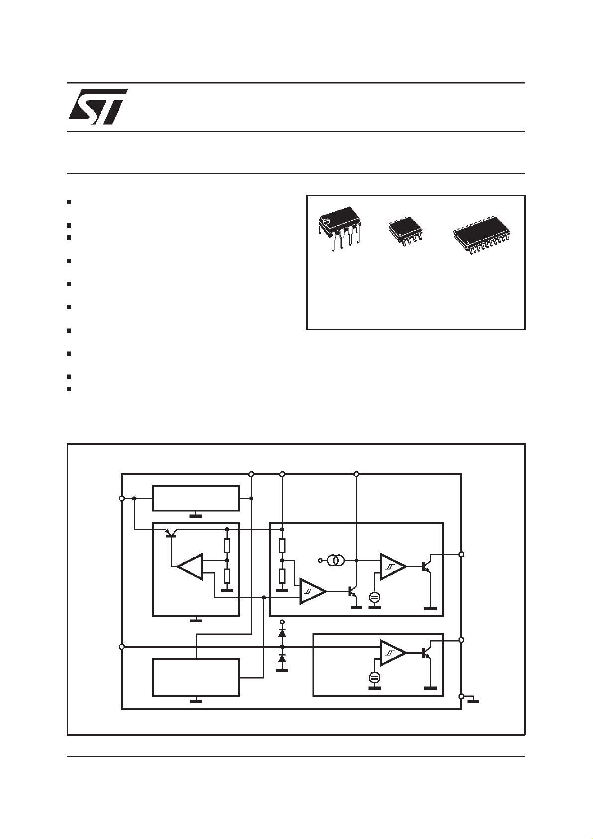
BLOCK DIAGRAM
S
SI
PREREGULATOR 5VV
REG
REF
1.23V
V
OUT
Z
+
RESET
V
S
SENSE
CTV
2µ
2V
1.23V
D96AT219
RES
SO
GND
June 2000
1/10
L4949E
ABSOLUTE MAXIMUM RATINGS
Symbol Parameter Value Unit
V
SDC
V
STR
I
V
V
RES,VSO
I
RES,ISO
V
I
T
T
Note: The circuit is ESD protectedaccording to MIL-STD-883C
THERMAL DATA
Symbol Description Minidip SO-8 SO20L Unit
R
th j-amb
R
thj-pins
TJSD Thermal Shutdown Junction temperature 165
DC Operating Supply Voltage 28 V
Transient Supply Voltage(T < 1s) 40 V
Output Current Internally Limited
O
Output Voltage 20 V
O
Output Voltage 20 V
Output Current 5 mA
Preregulator Output Voltage 7 V
Z
Preregulator Output Current 5 mA
Z
Junction Temperature -40 to +150
J
Storage Temperature Range -55 to +150 °C
stg
Thermal Resistance Junction-ambient Max 100 200 50 °C/W
Thermal Resistance Junction-pins Max 15 °C/W
C
°
C
°
PIN CONNECTIONS
V
S
SI
V
Z
CT GND
1
2
3
4
D95AT217
MINIDIP/SO8
V
Z
CT
N.C.
8
7
6
5
V
OUT
SO
RES
GND
GND
GND
GND
N.C.
N.C. V
RES SO
2
3
4
5
6
7
8
9
10
D95AT218
20
19
18
17
16
15
14
13
12
11
SI1
V
S
N.C.
GND
GND
GND
GND
N.C.
OUT
SO20
2/10
L4949E
ELECTRICALCHARACTERISTICS
= 14V; -40°C<Tj< 125°Cunless otherwisespecified)
(V
S
Symbol Parameter Test Condition Min. Typ. Max. Unit
V
V
V
V
DP
V
Output Voltage TJ=25°C; IO= 1mA 4.95 5 5.05 V
O
Output Voltage 6V < VIN<28V, 1mA < IO<50mA 4.90 5 5.10 V
O
Output Voltage VIN=40V;
O
Dropout Voltage IO= 10mA
Input to Output Voltage
IO
T<1s5mA<I
I
= 50mA
O
I
= 100mA
O
V
= 4V, IO= 35mA 0.4 V
IN
<100mA
O
4.75 5.25 V
0.1
0.2
0.3
0.25
0.4
0.5
Difference in Undervoltage
Condition
I
** Max Output Leakage VIN= 25V, VO= 5.5V 20 50 80 µA
outh
V
OL
V
OLO
I
LIM
I
QSE
I
Q
** With thistest we guaranteethat with no output currentthe output voltage will not exceed 5.5V
Line Regulation 6V < VIN< 28V; IO= 1mA 20 mV
Load Regulation 1mA < IO< 100mA 30 mV
Current Limit VO= 4.5V
V
= 4.5V, TJ=25°C
O
V
= 0V (note1)
O
105
120
200
100
400
400
Quiescent Current IO= 0.3mA; TJ< 100°C 200 300
Quiescent Current IO= 100mA 5 mA
RESET
V
V
t
V
I
V
V
CTth, hy
RT
RTH
RD
RL
RH
CTth
Reset Thereshold Voltage VO-0.5 V V
Reset Thereshold Hysteresis 50 100 200 mV
Reset Pulse Delay CT= 100nF; TR≥100µs 55 100 180 ms
Reset Output Low Voltage R
ResetOutput High Leakage Current V
= 10KΩto VOV
RES
=5V 1
RES
1.5V 0.4 V
≥
S
Delay Comparator Thereshold 2 V
Delay Comparator Thereshold
100 mV
Hysteresis
SENSE
V
V
V
mA
mA
mA
µ
µ
A
A
V
V
sth
V
SL
I
SH
I
SI
Sense Low Thereshold 1.16 1.23 1.35 V
st
Sense Thereshold Hysteresis 20 100 200 mV
Sense Output Low Voltage V
Sense Output Leakage VSO= 5V; VSI≥ 1.5V 1 µA
Sense Input Current VSI= 0 -20 -8 -3 µA
PREREGULATOR
V
I
Note 1: Foldback characteristic
Preregulator Output Voltage IZ=10µA 4.5 5 6 V
Z
Preregulator Output Current 10
Z
≤
SI
R
= 10KΩ to V
SO
1.16V;V
3V
≥
S
O
0.4 V
A
µ
3/10

L4949E
APPLICATIONCIRCUIT
V
OUT
V
(optional)
Z
V
BAT
For stability: C
Recommendedfor application:C
V
S
SI
≥ 1µF, CO≥ 4.7µF, ESR< 10Ω at 10KHz
S
PREREGULATOR 5V
REG
REF
S=CO
1.23V
=10µF to 100µF
APPLICATIONINFORMATION
Supply Voltage Transient
High supplyvoltage transients can cause a reset
output signaldisturbation.
For supply voltages greater than 8V the circuit
shows a high immunity of the reset outputagainst
supply transientsof morethan100V/µs.
For supply voltages less than 8V supply transients of more than 0.4V/µs can cause a reset
signal disturbation.
To improve the transient behaviour for supply
voltages less than 8V a capacitor at pin 3 can be
used.
A capacitor at pin 3 (C3 ≤ 1µF) reduces also the
output noise.
CT
GND
RES
V
SO
OUT
RESET
V
2µ
+
2V
S
1.23V
SENSE
D96AT219
proach of this device allows to get easily also
other featuresand functions when required.
Voltage Regulator
The voltage regulator uses an Isolated Collector
Vertical PNP transistor as a regulating element.
Figure1: FoldbackCharacteristic of V
O
FUNCTIONAL DESCRIPTION
The L4949E is a monolithic integrated voltage
regulator, based on the STM modular voltage
regulator approch. Several outstanding features
and auxiliary functions are implemented to meet
the requirements of supplying microprocessor
systems in automotive applications.Nevertheless,
it is suitable also in other applications where the
present functions are required. The modular ap-
4/10

L4949E
With this structure very low dropout voltage at
currents up to 100mA is obtained. The dropout
operation of the standby regulator is maintained
down to 3V input supply voltage. The output voltage is regulated up to the transient input supply
voltage of 40V. With this feature no functionalinterruptiondue to overvoltagepulses is generated.
The typical curve showing the standby output
voltage as a functionof theinput supply voltage is
shown in Fig. 2. The current consumption of the
device (quiescentcurrent) is less than 300µA.
To reduce the quiescent current peak in the undervoltage region and to improvethe transientresponse in this region, the dropout voltage is controlled, the quiescent current as a function of the
supply input voltage is shown inFig. 3.
Figure 2:
OutputVoltage vs. Input Voltage
Preregulator
To improve the transient immunity a preregulator
stabilized the internal supply voltage to 5V. This
internal voltage is present at Pin3 (V
). This volt-
Z
age should not be usedas an output because the
output capabilityis very small (≤10µA).
This output may be used as an option when a
better transient behaviour for supplyvoltages less
than 8V is required (see alsoapplication note).
In this case a capacitor (100nF - 1µF) must be
connectedbetween Pin 3 andGND. If thisfeature
is not used Pin 3 must be left open.
Reset Circuit
The block circuit diagram of the reset circuit is
shown in Fig. 4. The reset circuit supervises the
output voltage.
The reset thereshold of 4.5V is defined with the
internal reference voltage and standby output
drivider.
The reset pulse delay time t
chargetime of an externalcapacitor C
C
=
t
RD
, is definedwith the
RD
• 2V
T
2µA
:
T
40V
Figure 3: QuiescentCurrent vs. Supply Voltage
The reaction time of the reset circuit originates
from the discharge time limitation of the reset capacitorC
and is proportionalto the value of CT.
T
The reaction time of thereset circuit increases the
noise immunity. Standbyoutput voltagedrops below the reset threshold only a bit longer than the
reactiontime results in a shorterreset delay time.
The nominal reset delay time will be generated for
standbyoutput voltage drops longer than approximately 50µs.
The typical reset output waveforms are shown in
Fig. 5.
Sense Comparator
The sense comparator compares an input signal
with an internalvoltage reference of typical1.23V.
The use of an external voltage divider makes this
comparatorvery flexible in the application.
It can be used to supervise the input voltage
either before or after the protection diode and to
give additional informationsto the microprocessor
likelow voltagewarnings.
5/10

L4949E
Figure 4
Figure 5
6/10

L4949E
DIM.
MIN. TYP. MAX. MIN. TYP. MAX.
A 3.32 0.131
a1 0.51 0.020
B 1.15 1.65 0.045 0.065
b 0.356 0.55 0.014 0.022
b1 0.204 0.304 0.008 0.012
D 10.92 0.430
E 7.95 9.75 0.313 0.384
e 2.54 0.100
e3 7.62 0.300
e4 7.62 0.300
F 6.6 0.260
I 5.08 0.200
L 3.18 3.81 0.125 0.150
Z 1.52 0.060
mm inch
OUTLINE AND
MECHANICAL DATA
Minidip
7/10

L4949E
DIM.
MIN. TYP. MAX. MIN. TYP. MAX.
A 1.75 0.069
a1 0.1 0.25 0.004 0.010
a2 1.65
a3 0.65 0.85 0.026 0.033
b 0.35 0.48 0.014 0.019
b1 0.19 0.25 0.007 0.010
C 0.25 0.5 0.010 0.020
c1 45° (typ.)
D (1) 4.8 5.0 0.189 0.197
E 5.8 6.2 0.228 0.244
e 1.27 0.050
e3 3.81 0.150
F (1) 3.8 4.0 0.15 0.157
L 0.4 1.27 0.016 0.050
M 0.6 0.024
S8°(max.)
(1) D andF do not include moldflash or protrusions. Mold flash or
potrusions shallnot exceed 0.15mm(.006inch).
mm inch
0.065
OUTLINE AND
MECHANICAL DATA
SO8
8/10

L4949E
DIM.
MIN. TYP. MAX. MIN. TYP. MAX.
A 2.35 2.65 0.093 0.104
A1 0.1 0.3 0.004 0.012
B 0.33 0.51 0.013 0.020
C 0.23 0.32 0.009 0.013
D 12.6 13 0.496 0.512
E 7.4 7.6 0.291 0.299
e 1.27 0.050
H 10 10.65 0.394 0.419
h 0.25 0.75 0.010 0.030
L 0.4 1.27 0.016 0.050
K0°(min.)8°(max.)
mm inch
OUTLINEAND
MECHANICALDATA
SO20
B
e
D
1120
110
L
hx45°
A
K
A1
C
H
E
SO20MEC
9/10

L4949E
Information furnished is believed to be accurate and reliable. However, STMicroelectronics assumes no responsibility for the consequences
of use of such information nor for any infringement of patents or other rights of third parties which may result from its use. No license is
granted by implicationor otherwise under any patent or patent rights of STMicroelectronics. Specification mentioned in this publication are
subject to change without notice. This publication supersedes and replaces all information previously supplied. STMicroelectronics products
are not authorized for use as critical components in lifesupport devices or systems without express written approval of STMicroelectronics.
The ST logois a registeredtrademark of STMicroelectronics
2000 STMicroelectronics – Printed in Italy – All Rights Reserved
STMicroelectronics GROUP OF COMPANIES
Australia - Brazil - China - Finland - France - Germany - Hong Kong - India - Italy - Japan - Malaysia - Malta - Morocco -
Singapore - Spain - Sweden- Switzerland - United Kingdom- U.S.A.
http://www.st.com
10/10
 Loading...