

L4941
April1994
VERY LOW DROP 1A REGULATOR
.LOWDROPOUTVOLTAGE (450mV typ
at1A)
.VERYLOW QUIESCENT CURRENT
.THERMALSHUTDOWN
.SHORTCIRCUITPROTECTION
.REVERSE POLARITY PROTECTION
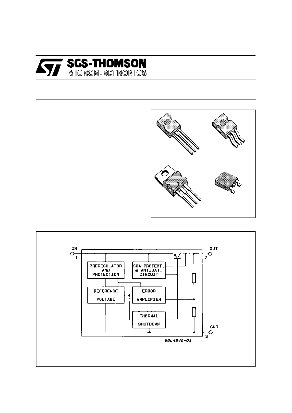
DESCRIPTION
The L4941is a threeterminal 5 V positive regulator
available in TO-220,SOT-82, SOT-194 and DPAK
packages, making it useful in a wide range of the
industrial and consumer applications. Thanks to its
very low input/output voltage drop, this device is
particularlysuitable forbatterypoweredequipment,
reducing consumptionand prolonging batterylife.It
employs internal current limiting, antisaturation
circuit,thermal shut-downand safeareaprotection.
TO-220 DPAK (TO-252)
BLOCK DIAGRAM
SOT-82 SOT-194
1
3
1/13
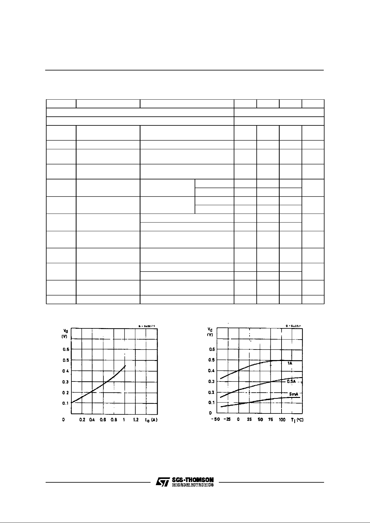
ABSOLUTE MAXIMUM RATINGS
Symbol Paramet e r Valu e Unit
V
i
Forward Input Voltage 30 V
V
iR
Reverse Input Voltage (RO= 100 Ω)–15V
I
O
Output Current Internally Limited
P
tot
Power Dissipation Internally Limited
T
j,Tstg
Junction and Storage Temperature – 40 to 150 °C
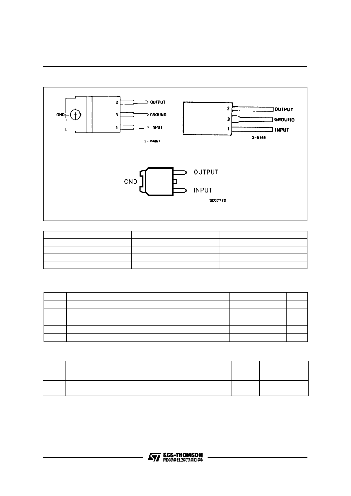
PIN CON NEC TIONS AND ORDERI NG NUMBER (top view)
THERMAL DATA
SOT-82
SOT-194
DPAK
TO-220
R
thj-case
Thermal Resistance Junction-case Max 8 3
o
C/W
R
thj-amb
Termalresistance Junction-ambient Max 100 50
o
C/W
TO-220 SOT-82/SOT-194
ORDERING NUMBERS OUTPUT VOLTAGE PACKAGE
L4941BV 5V TO-220
L4941BX 5V SOT-82
L4941BS 5V SOT-194
L4941BDT 5V DPAK
DPAK
L4941
2/13
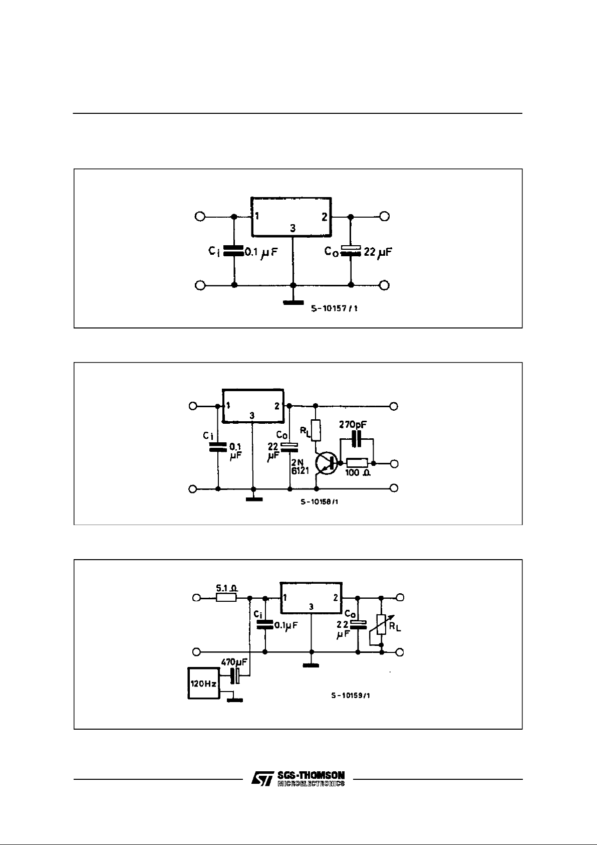
Figure 2 : LoadRegulation.
Figure 3 : RippleRejection.
Figure 1 : DCParameters.
TEST CIRCUITS
L4941
3/13
ELECTRICAL CHARACTERISTICS (refer to the test circuits Tj=25°C,Ci= 0.1 µF, Co=22µF,
unless otherwise specified)
Symbol P arameter Test Conditions Min. Typ. Max. Unit
Output Voltage 5
Input Voltage (unless otherwise specified) 7
V
o
Output Voltage Io= 5 mA to 1 A
Vi=6Vto14V
4.8 5 5.2 V
V
i
Operating Input Voltage Io= 5 mA 16 V
∆V
o
Line Regulation Vi=6Vto16V
Io=5mA
520mV
∆V
o
Load Regulation Io= 5 mA to 1 A
Io= 0.5 A to 1 A
8
5
20
15
mV
I
Q
Quiescent Current Io=5mA 4 8
V
i
=6V
I
o
=1A 20 40
mA
∆I
Q
Quiescent Current
Change
Io= 5 mA 3
V
i
=6Vto14V
I
o
=1A –10
mA
V
d
Dropout Voltage Io= 0.5 A 250 450
I
o
= 1 A 450 700
mV
∆V
o
____
∆T
Output Voltage Drift 0.6 mV/°C
SVR Supply Voltage
Rejection
f = 120 Hz
I
o
= 0.5 A
58 68 dB
I
sc
Short Circuit Current
Limit
Vi= 14 V 1.6 2.0
V
i
= 6 V 1.8 2.2
A
Z
o
Output Impedance f = 1 kHz
I
o
= 0.5 A
30 mΩ
e
N
Output Noise Voltage B = 100 Hz to 100 kHz 30 µV/V
o
Figure 4 : Dropoutvoltage vs.Output Current. Figure5 : Dropout Voltage vs. Temperature.
L4941
4/13

Figure 6 : Outputvoltage vs. Temperature. Figure7 : Quiescent Current vs. Temperature
Figure 8 : Quiescent Current vs.InputVoltage. Figure9 : Quiescent Current vs.Output Current.
Figure 10: Short-circuit Current vs. Temperature. Figure11 : Peak Output Current vs. Input/Output
DifferentialVoltage.
L4941
5/13

Figure 12: LowVoltage Behavior. Figure13 : Supply Voltage Rejection vs.
Frequency
Figure 14: Supply Voltage Rejection vs.Output
Current.
Figure15 : Load DumpCharacteristics.
Figure 16: LineTransientResponse. Figure17 : Load Transunt Response.
L4941
6/13

Figure 18: TotalPowerDissipation (TO-220).
Figure 19: Distribued Supply with On-card L4940 and L4941 Low-drop Regulators.
ADVANTAGES OF THESE APPLICATIONS ARE :
-
On card regulation with short-circuit and thermal protection oneach output.
-
Very hightotalsystemefficiencydueto the switchingpreregulation and verylow-drop postregulations.
L4941
7/13
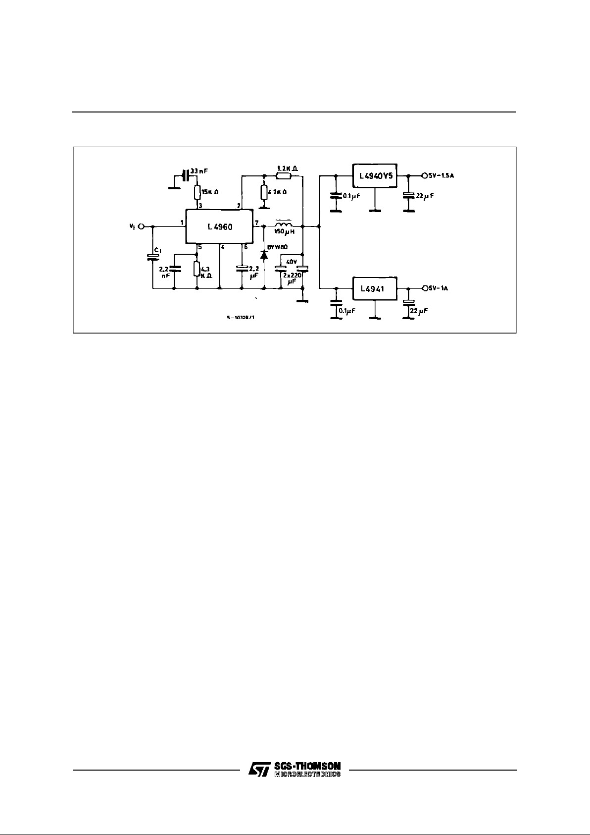
Figure 20 : Distribued Supply with On-card L4940 and L4941 Low-drop Regulators.
L4941
8/13
DIM.
mm inch
MIN. TYP. MAX. MIN. TYP. MAX.
A 4.8 0.189
C 1.37 0.054
D 2.4 2.8 0.094 0.110
D1 1.2 1.35 0.047 0.053
E 0.35 0.55 0.014 0.022
F 0.8 1.05 0.031 0.041
F2 1.15 1.4 0.045 0.055
G 4.95 5.08 5.21 0.195 0.200 0.205
H2 10.4 0.409
H3 10.05 10.4 0.396 0.409
L2 16.2 0.638
L3 26.3 26.7 27.1 1.035 1.051 1.067
L5 2.6 3 0.102 0.118
L6 15.1 15.8 0.594 0.622
L7 6 6.6 0.236 0.260
Dia. 3.65 3.85 0.144 0.152
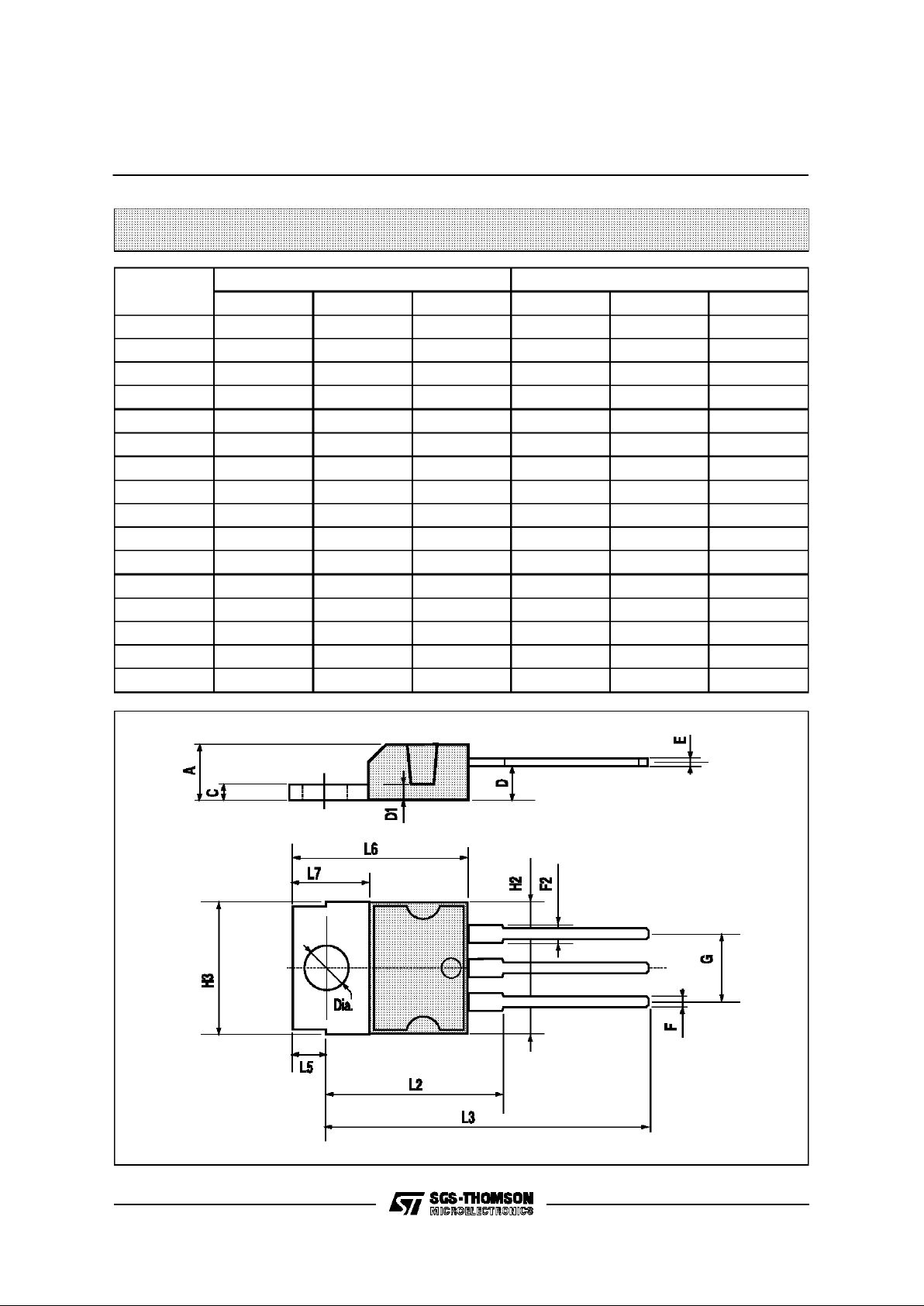
TO-220 MECHANICAL DATA
P011D
L4941
9/13
DIM.
mm inch
MIN. TYP. MAX. MIN. TYP. MAX.
A 7.4 7.8 0.291 0.307
B 10.5 11.3 0.413 0.445
b 0.7 0.9 0.028 0.035
b1 0.49 0.75 0.019 0.030
C 2.4 2.7 0.04 0.106
c1 1.2 0.047
D 15.7 0.618
e 2.2 0.087
e3 4.4 0.173
F 3.8 0.150
H 2.54 0.100
F
A
H
BD
e3
e
b1
c1
C
b
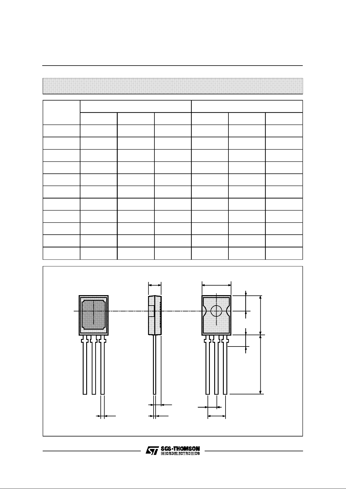
SOT-82 MECHANICALDATA
P032A
L4941
10/13

DIM.
mm inch
MIN. TYP. MAX. MIN. TYP. MAX.
A 7.4 7.8 0.291 0.307
B 10.5 11.3 0.413 0.445
b 0.7 0.9 0.028 0.035
b1 0.49 0.75 0.019 0.030
C 2.4 2.7 0.094 0.106
c1 1.2 0.047
c2 1.3 0.051
D 6 0.236
e 2.2 0.087
e3 4.4 0.173
F 3.8 0.150
H 2.54 0.100
P45°(typ.)
S 4 0.157
S1 2 0.079
T 0.1 0.004
F
A
H
B
D
e3
e
b1
c2
C
b
P
T
C1
SS1
SOT-194 MECHANICALDATA
P032B
L4941
11/13
DIM.
mm inch
MIN. TYP. MAX. MIN. TYP. MAX.
A 2.2 2.4 0.086 0.094
A1 0.9 1.1 0.035 0.043
B 0.64 0.8 0.025 0.031
B1 3.4 3.6 0.133 0.141
B2 5.2 5.4 0.204 0.212
B3 0.9 0.035
B4 1.9 2.1 0.074 0.082
C 0.48 0.6 0.018 0.023
C1 0.45 0.6 0.017 0.023
D 6 6.2 0.236 0.244
E 6.4 6.6 0.252 0.260
G 4.4 4.6 0.173 0.181
H 9.35 10.1 0.368 0.397
L 2.55 3.05 0.100 0.120
L1 0.6 1 0.023 0.039
L2 0.8 0.031
L3 0.8 1.2 0.031 0.047
L4 0.3 0.45 0.012 0.017
D
A
C
C1
L
L2
= G =
L1
L4
H
A1
L3
123
==
==
==
==
B
B3
B2EB1
B4
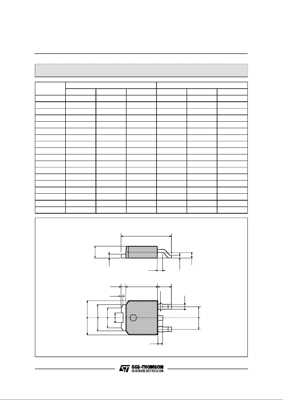
TO-252 (DPAK) MECHANICAL DATA
L4941
12/13

Information furnishedis believed to be accurateand reliable.However, SGS-THOMSON Microelectronics assumesno responsability for the
consequences of useof such informationnor for any infringement of patentsor otherrights ofthird partieswhich may results fromits use. No
license is granted by implication or otherwise underany patentor patent rights ofSGS-THOMSON Microelectronics.Specificationsmentioned
in thispublication aresubject to changewithout notice.This publicationsupersedes and replaces all informationpreviously supplied.
SGS-THOMSON Microelectronicsproductsare not authorizedfor use ascritical componentsin life support devicesor systems without express
written approval of SGS-THOMSONMicroelectonics.
1994 SGS-THOMSON Microelectronics - All Rights Reserved
SGS-THOMSON MicroelectronicsGROUP OFCOMPANIES
Australia - Brazil - France- Germany - HongKong - Italy - Japan - Korea - Malaysia- Malta - Morocco - The Netherlands-
Singapore- Spain - Sweden- Switzerland - Taiwan- Thailand - United Kingdom- U.S.A
L4941
13/13
 Loading...