

L4938N/ND
DUAL MULTIFUNCTIONVOLTAGE REGULATOR
.STANDBYOUTPUTVOLTAGEPRECISION5V
± 2%
.
OUTPUT2TRACKEDTOTHESTANDBYOUTPUT
.
OUTPUT 2 DISABLE FUNCTION FOR
STANDBYMODE
.VERY LOW QUIESCENT CURRENT, LESS
THAN 250µA,IN STANDBYMODE
.OUTPUT 2 VOLTAGESETTABLEFROM5 TO
20V
.OUTPUTCURRENTS: I
.
VERYLOWDROPOUT(max 0.4V/0.6V)
=50mA,I02=500mA
01
.OPERATINGTRANSIENT SUPPLYVOLTAGE
UP TO 40V
.POWER-ON RESET CIRCUIT SENSING THE
STANDBYOUTPUT VOLTAGE
.
POWER-ONRESET DELAY PULSEDEFINED
BY THE EXTERNALCAPACITOR
.
EARLYWARNINGOUTPUTFORSUPPLYUNDERVOLTAGE
.
THERMALSHUTDOWNAND SHORTCIRCUIT
PROTECTIONS
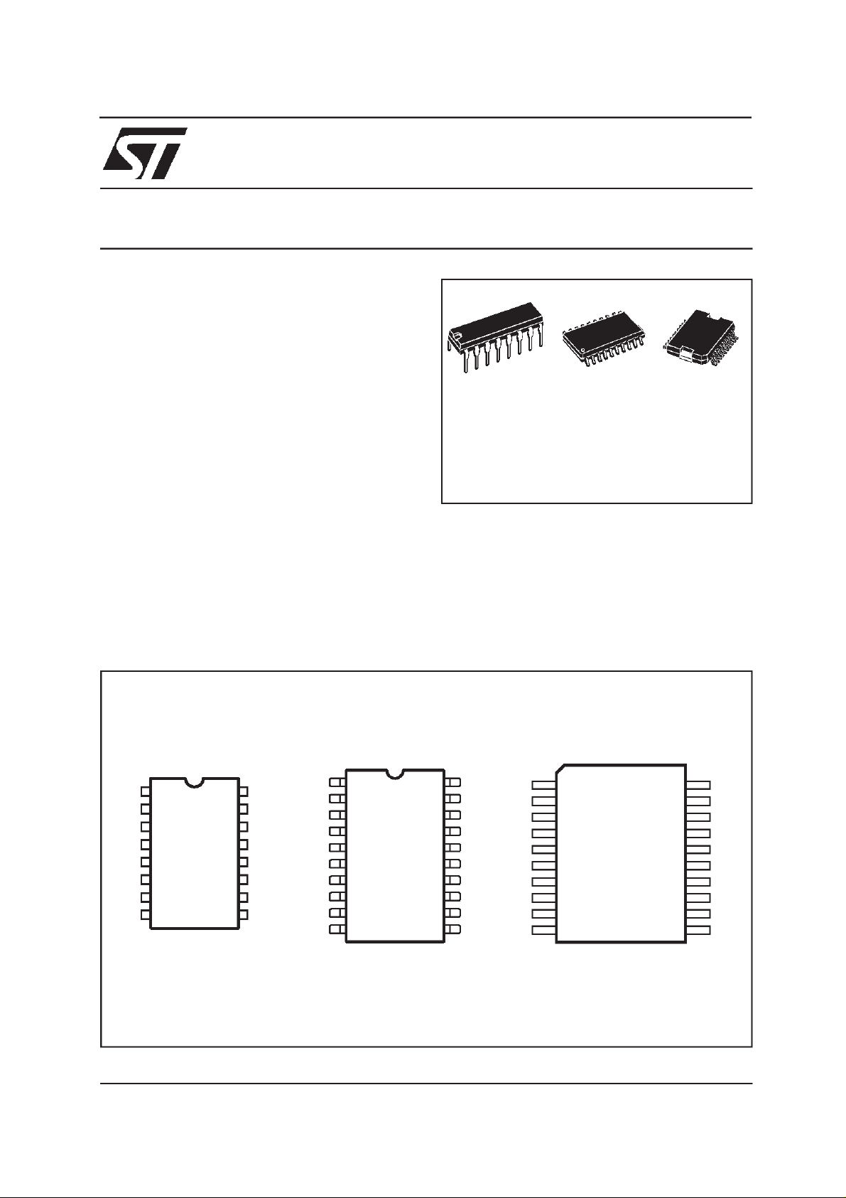
PI N CONNECTION
(top view)
L4 938N PD
PowerDIP
(12+2+2)
ORDERINGNUMBERS: L4938N (PDIP)
DES CRIPTI ON
The L4938Nis a monolithicintegrateddualvoltage
regulatorswithtwoverylowdropoutoutputsandadditionalfunctionssuchas power-onresetand input
voltagesense.Theyare designedfor supplyingmicrocomputer controlled systems specially in automotiveapplications.
SO20
(12+4+4)
L4938ND(SO)
L4938NPD (PSO20)
PowerSO20
POWERDIP
N.C.
GND
GND
RES
V
April 1999
This is advanced information on a new product now in development or undergoing evaluation. Details are subject to change without notice.
1
CT
2
EN
3
4
5
6
SO
7V
8 ADJ9
O1
D95AT156
SI16
V
15
V
14
GND
13
GND
12
V
11
10
N.C.
S1
S2
O2
O2
C7
EN
GND
GND
GND
GND
RES
SO
V
O1
SO20
1
2
3
4
5
6
7
8
9
10
D93AT004
20
19
18
17
16
15
14
13
12
11
SI
V
S1
VS2
GND
GND
GND
GND
VO2
V
O2
ADJ
GND
N.C.
V
S2
V
S1
SI
N.C.
CT
EN
N.C.
GND 10
PowerSO20
1
2
3
4
5
6
7
8
9
D95AT169A
20
19
18
17
16
15
14
13
12
11
GND
N.C.
V
O2
ADJ
V
O1
SO
RESET
N.C.
N.C.
GND
1/12
L4938N - L4938ND - L4938NPD
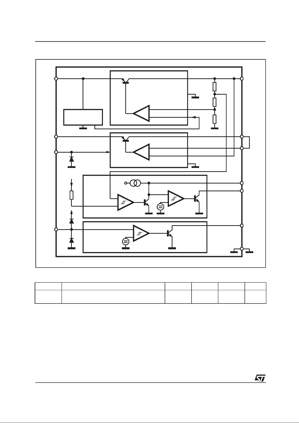
BLOCK DIAG RAM
V
V
EN
S1
REFERENCE
S2
REG1
1.23V
V
O1
V
O2
ADJ
REG2
1.23V
RESET
2µ
2.0V
CT
RES
SI
SENSE
1.23V
(optional)
D94AT143A
THERMAL DATA
Symbol Parameter Powerdip PowerSO20 SO20 Unit
R
thj-case
R
thj-amb
ThermalResistance Junction-Case Max.
ThermalResistance Junction-Ambient Max.
14
90
<2
–
–
20
SO
GND
°
°C/W
C/W
2/12
L4938N - L4938ND - L4938NPD
ABSOLUTE MAXIMUM RATINGS
Symbol Parameter Value Unit
V
T
j,Tstg
I
SI
I
EN
V
EN
V
RES,VSO
I
RES,ISO
P
The circuit is ESD protected according to MIL–STD–883C.
Note :
APPLI CATI ON CIRCUI T
DC Supply Voltage 28 V
S
TransientSupply Voltage (T < 1s) 40 V
Junctionand Storage Temperature Range –55 to 150
Sense Input Current (V
≤
SI
0.3V or V
SI>VS
)
1
±
Enable Input Current (VEN≤0.3V) ±1
Enable Input Voltage V
S
Reset and Sense Output Voltage 20 V
Reset and Sense Output Current 5 mA
Power Dissipation 875 mW
D
°
mA
mA
C
V
S1
C
S
REFERENCE
V
S2
EN
1.23V
RESET
SI
SENSE
(optional)
REG1
REG2
1.23V
CS≥ 1µF;C01≥ 6µF;C02≥ 10µF, ESR < 10Ω at 10KHz
V
O1
C
O1
1.23V
V
O2
ADJ
C
O2
CT
CT
2µ
2.0V
D94AT144A
RES
SO
GND
R
RES
V
O1
R
SO
3/12
L4938N - L4938ND - L4938NPD
ELECTRICAL CHARACTERISTICS (VS= 14V; –40°C ≤ TJ≤ 125°C unlessotherwise specified)
Symbol Parameter Test Conditions Min. Typ. Max. Unit
V
V
V
O2-VO1
I
ADJ
V
DP1
V
V
DP2
V
V
OL 1.2
V
OLO1
V
OLO2
I
LIM1
I
LIM2
I
QSB
I
Operating Supply Voltage 25 V
S
StandbyOutput Voltage
O1
Output Voltage 2 TrackingError
(note 1)
6V ≤ V
1mA≤I
6V≤V
5mA≤I
≤ 25V
S
O1
≤
S
O2
50mA
≤
25V
500mA
≤
4.90 5.00 5.10 V
–25 +25 mV
Enable= LOW
ADJ InputCurrent IO1= 1mA; IO2= 5mA –1 0.1 1
DropoutVoltage 1 IO1= 10mA
Inputto OutputVoltage
IO1
I
= 50mA
O1
VS = 4V,IO1= 35mA 0.4 V
0.1
0.2
Differencein Undervoltage
Condition
DropoutVoltage 2 IO1 = 100mA
Inputto OutputVoltage
IO2
I
= 500mA
O1
VS = 4.6V,IO1= 350mA 0.6 V
0.2
0.3
Differencein Undervoltage
Condition
LineRegulation
6V ≤ V
I
Load Regulation 1
Load Regulation 2
1mA≤I
5mA≤I
Current Limit 1 VO1= 4.5V
V
≤ 25V
S
= 1mA; IO2= 5mA
O1
50mA
≤
O1
500mA
≤
O2
= 0V(note 2)
O1
55
25
100
50
Current Limit 2 VO2 = 0V 550 1000 1700 mA
Quiescent Current StandbyMode
(output2 disabled)
Quiescent Current IO1= 50mA
Q
I
= 0.3mA;TJ< 100°C
O1
2.4V
V
≥
EN
V
= 14V
S
V
= 3.5V
S
I
= 500mA
O1
210
340
0.25
0.4
0.3
0.6
20 mV
25 mV
50 mV
200
100
290
850
30 mA
µA
V
V
V
V
mA
mA
µ
µA
A
ENABLE
V
ENL
V
ENH
V
ENhyst
I
EN
4/12
EnableInput LOW Voltage
–0.3 1.5 V
(output2 active)
EnableInput HIGH Voltage 2.4 7 V
EnableHysteresis 30 75 200 mV
EnableInput Current 0V < VEN< 1.2V
2.5V < V
EN
<7V
–10–1–1.50–0.5
+1
µ
µ
A
A

L4938N - L4938ND - L4938NPD
ELECTRICAL CHARACTERISTICS (continued)
RESET
Symbol Parameter Test Conditions Min. Typ. Max. Unit
V
V
t
RD
t
RR
V
I
LRES
V
CTh
V
CTh, hyst
SENSE
ResetLow Threshold Voltage Vo1-0.4 4.7 Vo1-0.1 V
Rt
ResetThreshold Hysteresis 50 100 200 mV
Rth
ResetPulse Delay
ResetReaction Time CT= 100nF 1 10 50
ResetOutput LOW Voltage
RL
ResetOutput HIGH Leakage V
Delay Comparator Threshold 2.0 V
Delay Comparator Threshold
Hysteresis
= 100nF;tR> 100µs
C
T
= 10KΩto V
R
RES
VS= 1.5V
=5V 1 µ
RES
01
55 100 180 mV
100 mV
0.4 V
µs
A
V
Note :
V
Slth,hyst
V
SOL
I
LSO
Sense Threshold Voltage 1.16 1.23 1.35 V
Slth
Sense Threshold Hysteresis 40 100 200 mV
Sense Output LOW Voltage
Sense Output Leakage
1:V
connected toADJ.VO2canbe setto higher values by inserting an externalresistor divider.
O2
2 : Foldbackcharacteristic
=1,16V; V
V
SI
R
=10KΩto V
SO
= 5V;V
V
SO
FUNCTI O NAL DESCRI P TION
The L4938N is based on the STMicroelectronics
modular voltage regulator approach. Several outstanding features and auxiliary functions are providedtomeettherequirementsofsupplyingthemicroprocessor systemsused in automotiveapplications.
Furthermorethe deviceis suitablealso in otherapplications requiringtwo stabilizedvoltages.
The modular approach allows other features and
functionsto berealized easilywhen required.
STANDBYREGULATOR
The standby regulator uses an Isolated Collector
Vertical PNP transistor as the regulating element.
This structureallows a very low dropoutvoltageat
currentsup to 50mA.The dropoutoperation of the
standby regulator is maintained down to 2V input
supplyvoltage.The output voltageis regulatedup
tothetransientinputsupplyvoltageof40V.Thisfeatureavoidsfunctionalinterruptions whichcould be
generatedby overvoltagepulses.
Thetypicalcurveof thestandbyoutputvoltageas a
functionof theinputsupplyvoltageisshowninfig.1.
3V
≥
S
01
1.5V
≥
SI
0.4 V
1
The current consumption of the device (quiescent
current) is less than 250µA when output 2 is dis-
abled(standbymode). The dropoutvoltageis controlledto reduce the quiescentcurrent peak in the
undervoltage region and to improve the transient
responsein thisregion.
Thequiescentcurrentisshowninfig.2as afunction
of the supplyinputvoltage 2.
OUTPUT2 VOLTAGE
Theoutput2 regulatoruses the sameoutput struc-
tureas thestandbyregulator,butratedforanoutput
currentof 500mA.
The output2 regulatorworks in trackingmodewith
the standbyoutput voltage as a referencevoltage
when the output 2 programming pin ADJ is connectedto V
tothe pinADJ asshowninfig. 3, theoutputvolt-
R
2
. By connectinga resistordivider R1,
O2
age 2 can be programmedto thevalue :
V
O2=VO1
(1 + R1/R2)
The output 2 regulator can be switchedoff via the
Enableinput.
If a fixed5 regulationis requiredADJPin hasto be
connectedto V
02
Pin.
µ
A
5/12

L4938N - L4938ND - L4938NPD
Figure1 : OutputVoltagevs. InputVoltage.
Figure2 : QuiescentCurrentvs. SupplyVoltage.
400µ
200µ
Figure3 : ProgrammableOutput2 VoltagewithExternalResistors.
6/12

L4938N - L4938ND - L4938NPD
RESETCIRCUIT
Theblockcircuitdiagramoftheresetcircuitisshown
infig.4.Theresetcircuitsupervisesthe standbyoutput voltage.The reset thresholdof 4.7V is defined
by the internal reference voltage and the standby
outputdivider.
The reset pulse delay time t
chargetime ofan externalcapacitorC
x2V
C
T
=
t
RD
2µA
, is defined by the
RD
:
T
Thereactiontimeoftheresetcircuitdependson the
discharge time limitation of the reset capacitor C
andis proportionalto thevalue of CT.
The reactiontime of the resetcircuit increasesthe
noiseimmunity.In fact,if thestandbyoutputvoltage
drops below the reset threshold for a time shorter
thanthe reactiontime t
, no resetoutputvariation
RR
Figure 4: Block Diagram of the Reset Circuit.
occurs. The nominal reset delay is generated for
standbyoutput voltage drops longer thanthe time
necessary for the complete dischargingof thecapacitorC
C
T
. This time is typically equal to 50µsif
T
=100nF.The typicalresetoutputwaveformsare
shownin fig.5.
SENSECOMPARATOR
Thiscircuitcomparesaninputsignalwithan internal
voltagereference of typically1.23V. The use of an
externalvoltagedividermakesthecomparatorvery
flexiblein theapplication.Thisfunctioncanbe used
tosupervisetheinputvoltage- eitherbeforeorafter
theprotectiondiode- andtogiveadditionalinformationtothemicroprocessorsuchaslowvoltagewarn-
T
ings.
If this feature is not used SI and SO have to con-
nectedtoGND.In thiscasetheSt-byquiescentcurrent(14V) increasesfrom290µA to 300µA.
7/12

L4938N - L4938ND - L4938NPD
Figure5 : TypicalResetOutput Waveforms.
1.5V
8/12

L4938N - L4938ND - L4938NPD
DIM.
MIN. TYP. MAX. MIN. TYP. MAX.
a1 0.51 0.020
B 0.85 1.40 0.033 0.055
b 0.50 0.020
b1 0.38 0.50 0.015 0.020
D 20.0 0.787
E 8.80 0.346
e 2.54 0.100
e3 17.78 0.700
F 7.10 0.280
I 5.10 0.201
L 3.30 0.130
Z 1.27 0.050
mm inch
OUTLINE AND
MECHANICAL DATA
Powerdip 16
9/12

L4938N - L4938ND - L4938NPD
DIM.
MIN. TYP. MAX. MIN. TYP. MAX.
mm inch
A 3.6 0.142
a1 0.1 0.3 0.004
a2 3.3
0.012
0.130
a3 0 0.1 0.000 0.004
b 0.4 0.53 0.016 0.021
c 0.23 0.32 0.009 0.013
D (1) 15.8 16 0.622 0.630
D1 9.4 9.8 0.370 0.386
E 13.9 14.5 0.547 0.570
e 1.27 0.050
e3 11.43 0.450
E1 (1) 10.9 11.1 0.429 0.437
E2 2.9
0.114
E3 5.8 6.2 0.228 0.244
G 0 0.1 0.000 0.004
H 15.5 15.9 0.610 0.626
h 1.1
0.043
L 0.8 1.1 0.031 0.043
N10°(max.)
S
8°(max.)
T 10 0.394
(1) ”D andF” do notinclude mold flashor protrusions.
- Moldflash orprotrusions shall not exceed 0.15 mm (0.006”).
- Criticaldimensions: ”E”, ”G” and ”a3”
OUTLINE AND
MECHANICAL DATA
JEDEC MO-166
PowerSO20
E2
hx
45
DETAIL B
BOTTOM VIEW
R
Gage Plane
c
a1
E
L
DETAIL A
slug
-C-
SEATING PLANE
GC
(COPLANARITY)
E3
lead
a3
DETAIL B
0.35
S
D1
NN
a2
A
b
DETAIL A
e3
H
D
T
1
e
1120
E1
10
PSO20MEC
10/12

L4938N - L4938ND - L4938NPD
DIM.
MIN. TYP. MAX. MIN. TYP. MAX.
A 2.35 2.65 0.093 0.104
A1 0.1 0.3 0.004 0.012
B 0.33 0.51 0.013 0.020
C 0.23 0.32 0.009
D 12.6 13 0.496 0.512
E 7.4 7.6 0.291 0.299
e 1.27 0.050
H 10 10.65 0.394 0.419
h 0.25 0.75 0.010 0.030
L 0.4 1.27 0.016 0.050
K0°(min.)8°(max.)
mm inch
0.013
OUTLINE AND
MECHANICAL DATA
SO20
B
e
D
1120
110
L
hx45°
A
K
A1
C
H
E
SO20MEC
11/12

L4938N - L4938ND - L4938NPD
Information furnished is believed to be accurate and reliable. However, STMicroelectronics assumes no responsibility for the consequences of use of such information nor for any infringement of patents or other rights of third parties which may result from its use. No
license is granted by implication or otherwise under any patent or patent rights of STMicroelectronics. Specification mentioned in this
publication are subject to change without notice. This publication supersedes and replaces all information previously supplied. STMicroelectronics products are not authorized for use as critical components in life support devices or systems without express written
approval of STMicroelectronics.
Australia - Brazil - Canada - China - France - Germany - Italy - Japan - Korea - Malaysia - Malta - Mexico - Morocco - The Netherlands -
Singapore - Spain - Sweden - Switzerland - Taiwan - Thailand - United Kingdom - U.S.A.
The ST logo is a registered trademark of STMicroelectronics
1999 STMicroelectronics – Printedin Italy – All Rights Reserved
STMicroelectronics GROUP OF COMPANIES
http://www.st.com
12/12
 Loading...