

L4938E/ED
ADVANCEDVOLTAGE REGULATOR
ENABLE AND SENSE INPUTS (EN, SI) PROTECTED AGAINST NEGATIVE TRANSIENTS
DOWN TO-5V
RESET THRESHOLD ADJUSTABLE FROM
3.8 TO 4.7V
EXTREMELY LOW QUIESCENT CURRENT,
65µA (LESS THAN 90µA) IN STANDBY
MODE
OPERATINGDC SUPPLY VOLTAGE RANGE
5V -28V
OPERATING TRANSIENT SUPPLY VOLTAGE UP TO 40V
HIGHPRECISIONSTANDBYOUTPUTVOLTAGE 5V ± 1% WITH 100mA CURRENT CAPABILITY
OUTPUT 2 VOLTAGE 5V±2% WITH 400mA
CURRENT CAPABILITY (ADJ WIRED TO
V
)
OUT2
OUTPUT 2 VOLTAGE ADJUSTABLE BY EXTERNAL VOLTAGEDIVIDER
OUTPUT 2 DISABLE FUNCTION FOR
STANDBYMODE
L4938EPD
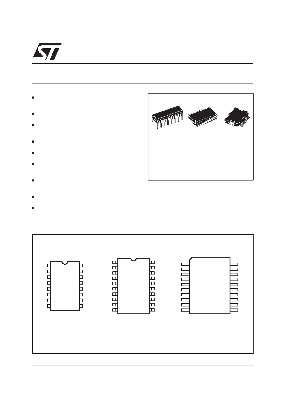
DIP (12+2+2) SO20 (12+4+4) PowerSO20
ORDERING NUMBERS:
DESCRIPTION
The L4938E/ED/EPD is a monolithic integrated
dual voltage regulator with two very low dropout
outputs and additional functions as power-on reset and input voltage sense. It is designed for
supplying the microcomputer controlled systems
especiallyin automotiveapplications.
L4938E (DIP)
L4938ED (SO)
L4938EPD (PSO)
PIN CONNECTIONS
PR
1
CT
2
EN
3
GND
GND
RES
OUT1 8 ADJ9
4
5
6
SO
7 OUT2
D94AT075A
DIP (12+2+2)
February 1999
15
14
13
12
11
10
SI16
VS1
VS2
GND
GND
N.C.
PR
CT
EN
GND
GND
GND
GND
RES
SO OUT2
OUT1 ADJ
2
3
4
5
6
7
8
9
10
D94AT076A
SI1
20
VS1
19
VS2
18
GND
17
GND
16
GND
15
GND
14
N.C.
13
12
11
SO (12+4+4)
GND
N.C.
V
S2
V
S1
SI
PR
CT
EN
N.C.
GND 10
1
2
3
4
5
6
7
8
9
PowerSO20
L4938EPD
20
19
18
17
16
15
14
13
12
11
GND
N.C.
OUT2
ADJ
OUT1
SO
RESET
N.C.
N.C.
GND
1/12
L4938E - L4938ED - L4938EPD
ABSOLUTE MAXIMUM RATINGS
Symbol Parameter Value Unit
V
INDC
V
INTR
I
O
V
SI
I
SI
V
EN
I
EN
V
RES,VSO
I
RES,ISO
P
O
T
stg
T
j
T
JSD
Note 1: The circuit is ESDprotected according to MIL-STD-883C
Note 2: Current forcedmeans voltage unlimited but current limited to the specified value
Voltageforced means voltage limitedtothe specified valueswhile the current is not limited
Note 3: Typicalvalue soldered on a PC board with 8cm
DC Operating Supply Voltage 28 V
Transient Operating Supply Voltage (T < 400ms) -14 to 40 V
Output Current internally limited
Sense Input Voltage (VoltageForced) (note 2) -20 to 20 V
Sense Input Current (Current Forced) (note 2)
1mA
±
Enable Input Voltage(Voltage Forced) (note 2) -20 to 20 V
Sense Input Current (Current Forced) (note 2)
1mA
±
Output Voltages -0.3 to 20 V
Output Currents (Output Low) 5 mA
Power Dissipation at T
=80°C (note 3)
amb
875 mW
Powerdip 12+2+2
Storage Temperature -65 to 150 °C
Operating Junction Temperature -40 to 150
Thermal shutdownjunction temperature Output 2 will shut-down
165
typically at Tj 10K lowerthan output 1
2
copperground plane (35mm thick).
C
°
C
°
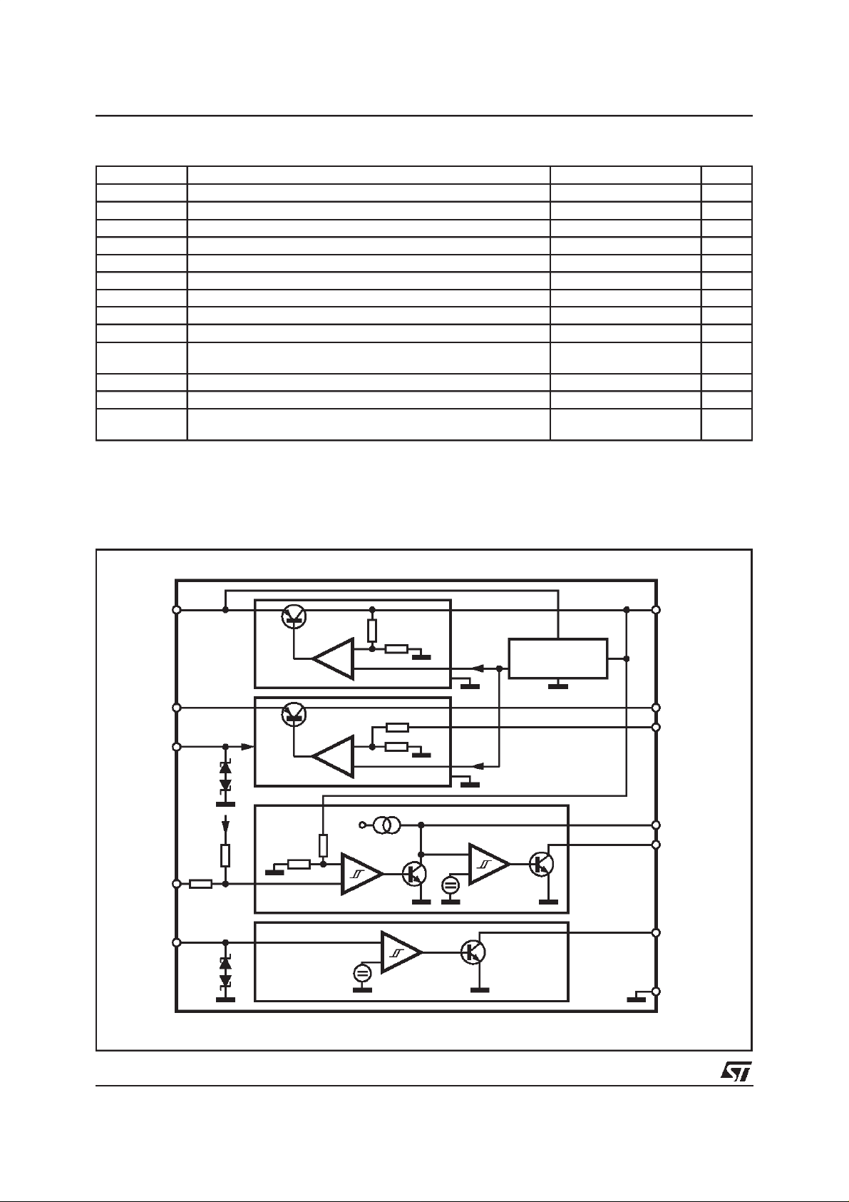
BLOCK DIAGRAM
VS1
VS2
EN
1.23V
PR
SI
REG1
REG2
RESET
OUT1
1.23V REFERENCE
OUT2
ADJ
1.23V
CT
RES
1.4V
SO
2/12
SENSE
1.23V
GND
D94AT074A
L4938E - L4938ED - L4938EPD
THERMAL DATA
Symbol Parameter DIP 12+2+2 SO 12+4+4 PowerSO20 Unit
R
th j-amb
R
th j-case
Note 3: Typicalvalue soldered on a PC board with 8cm2copperground plane (35mm thick).
PIN FUNCTIONS
Thermal ResistanceJunction to ambient 40 50 Thermal ResistanceJunction to case - - <2 °C/W
C/W
°
PIN
(DIP 12+2+2)
PIN
(SO 12+4+4)
PIN
PowerSO20
Name Function
14 18 3 VS2 Supply Voltage (400mA Regulator)
15 19 4 VS1 Supply Voltage (100mA Regulator, Reset, Sense)
16 20 5 S1 Sense Input
1 1 6 PR Reset Theresold Programming
2 2 7 CT Reset Delay Capacitor
3 3 8 EN Enable (low willactivate the 400mA regulator)
4, 5, 12, 13 4, 5, 6,7, 14,
1,10,11,20 GND Ground
15, 16, 17
6 8 14 RES Reset Output
7 9 15 SO Sense Output
8 10 16 OUT 1 100mA Regulator Output
9 11 17 ADJ Feedback of 400mA Regulator
10 12 18 OUT 2 400mA Regulator Output
11 13 2,9,19 NC Not Connected
ELECTRICALCHARACTERISTICS
= 14V; Tj=-40 to 150°C unless otherwise specified.)
(V
S
Symbol Parameter Test Condition Min. Typ. Max. Unit
OUT 1
V
V
V
V
I
O1
DP1
OL01
LIM1
QSB
Supply Output Voltage VS= 6 to 28V;
I
= 400µA to 100mA
O1
125°C; I
T
≤
Dropoutput Voltage 1 I
Load Regulation 1 I
j
OUT1
I
OUT1
OUT1
O1
= 10mA 0.1 0.2 V
= 100mA; VS= 4.8V 0.2 0.4 V
= 1 to 100mA
= 50 to 400µA 4.8 5 5.2 V
4.9 5 5.1 V
25 mV
(after regulation setting)
Current Limit 1 VOUT1 = 0.8 to 4.5V 100 200 400 mA
Quiescent Current in Standby
Mode
2.4V (output 2 disabled)
I
≥
EN
I
= 0.1mA; VSI> 1.3V
O1
<85°C;RPR=0 75 µA
T
J
65 90
OUT 2
V
V
V
R
I
O2
DP2
OL02
ADJ
LIM2
I
Q
Output Voltage 2
ADJ connected to OUT 2
Dropoutput Voltage 2 I
Load Regulation 2 I
Enable = LOW;VS= 6 to 28V;
I
= 5 to 400mA
02
= 100mA 0.2 0.3 V
OUT2
= 400mA; VS= 4.8V 0.3 0.6 V
I
OUT2
= 5 to 400mA
OUT1
4.9 5.1 V
50 mV
(after regulation setting)
Adjust Input Resistance 60 100 150 mA
Current Limit 2 V02 = 0.8 to 4.5V 450 650 1300 mA
Quiescent Current I
OUT1
= 100mA; I
= 400mA 20 mA
OUT2
OUT1,OUT 2
V
OLi 1,2
Line Regulation VS= 6 to 28V; IO1= 1mA,
I
= 5mA,
O2
(after regulation setting)
20 mV
A
µ
3/12
L4938E - L4938ED - L4938EPD
ELECTRICALCHARACTERISTICS
(Continued)
Symbol Parameter Test Condition Min. Typ. Max. Unit
ENABLE INPUT
V
ENL
V
ENH
V
ENhyst
I
EN LOW
I
EN HIGH
Enable Input Low Voltage
-20 1 V
(Output 2 Active)
Enable Input High Voltage 1.4 20 V
Enable Hysteresis 20 30 60 mV
Enable Input Current Low VEN= 0 -20 -8 -3 µA
Enable Input Current High VEN= 1.1 to 7V; TJ< 130°C; -1 0 1 µA
= 1.1 to 7V;
V
EN
T
= 130 to 150°C;
J
-10 0 10 µA
RESETCIRCUIT
V
RT
V
RTH
t
RD min
t
RD nom
t
RR
I
CT
I
CT
V
RESL
V
RESH
Reset Theresold Voltage
(note4)
Reset Theresold Hysteresis RPR=
Reset Pulse Delay C
Reset Pulse Delay C
Reset Reaction Time C
Pull Down Capability of the
RPR= ∞ 4.5 VO1-0.3 VO1-0.2 V
= 0 3.65 3.8 3.95 V
R
PR
∞
= 47nF; t
RES
= 47nF; (note 6) 60 100 140 ms
RES
= 47nF 10 50 150 µs
RES
V
OUT1<VRT
s; (note 5) 40 60 100 ms
≤30µ
r
30 60 120 mV
3615mA
Discharge circuit
Charge Current VOUT1 >VRT -1.3 -1 0.7 µA
Reset Output Low Voltage RRES = 10KΩ to VOUT1
1.5V
OUT1 ≥
=5V 1 µA
RES
Reset Output High Leakage
V
V
0.4 V
current
SENSECOMPARATOR
V
SI
V
SIT
V
SITH
V
SOL
I
SOH
I
SI HIGH
I
SI LOW
Note :
4) The reset threshold can be programmed continuously from typ 3.8V to 4.7V by changinga value of an external resistor frompin PR to GN
5) This is a minimum reset timeaccording to thehysteresis of the comparator. Delay timestarts with V
6) This is thenominal reset timedepending on the discharging limit of CT(saturationvoltage) and theupper threshold of the timer comparator.
Delay time starts with V
7) The leakage of CTmust be less than0.5mA (2V). If an externalresistor between CT and VOUT1is applied, the leakage current may be
increased. The external resistor should have more than 30KΩ.
for stability: Cs ≥ 1µF, C01 ≥ 10µF, C02 ≥ 10µF, ESR ≤ 5Ω (designed target) For details see application note.
8) For transients exceeding 20V or -20V externalprotection is required at the Pins SIand EN as shown at Pin EN. The protectionproposed will
provide proper function for transients in the range of ±200V. If the zener diode is omitted the external resistor should be raised to 200KΩ
to limit the current to 1mA. Without the zener diode, the function 20V or -20Vcan not be guaranteed.
Functional Range -20 20 V
Sense Threshold Voltage Falling Edge; TJ<130°C 1.08 1.16 1.24 V
Falling Edge; T
<130 to 150°C 1.05 1.16 1.29 V
J
Sense Threshold Hysteresis 10 30 60 mV
Sense Output Low Voltage VSI≤ 1.05V; RSO=10KΩ
connected to 5V; V
Sense Output Leakage VSO= 5V; V
SI ≥
5V
S ≥
1.5V 1
0.4 V
A
µ
Sense Input Current High VSI= 1.1 to 7V; TJ<130°C-101µA
= 1.1to 7V; TJ<130 to150°C -10 0 10 µA
V
SI
Sense Input Current Low VSI= 0V -20 -8 -3 µA
OUT1 exceeding VRT
OUT1
exceeding V
RT
4/12

Figure 1. ApplicationDiagram.
L4938E - L4938ED - L4938EPD
VS1
C
S
REG1
(Note 8)
100K
15V
for example
BZX97C15
VS2
EN
REG2
1.23V
PR
RESET
SI
1.23V
SENSE
FUNCTIONAL DESCRIPTION
The L4938E/ED/EPD is a monolithic integrated
dual voltage regulator, based on the STM modulator voltage regulator approach. Several outstanding features and auxiliary functions are implemented to meet the requirements of supplying
microprocessor systems in automotive applications. Nevertheless, it is suitable also in other applications where two stabilized voltages are required. The modular approach of this device
allows to get easly also other features and functions when required.
Standby Regulator
The standby regulator uses an Isolated collector
Vertical PNP transistor as a regulating element.
With this structure very low dropout volotage at
currents up to 100mA is obtained. The dropout
operation of the standby regulator is maintained
down to 3V input supply voltage. The output voltage is regulated up to the transient input supply
voltage of 40V. With this feature no functional interruptiondue to overvoltagepulses is generated.
In the standby mode when the output 2 is disabled, thecurrent consumptionof the device(quiescent current) is less than 90µA (14V supply
voltage).
OUT1
C
O1
1.23V REFERENCE
OUT2
C
CT (Note 7)
V
OUT1
R
SO
O2
ADJ
1.23V
CT
RES
1.4V
SO
GND
D94AT079A
To reduce the quiescent current peak in the undervoltage region and to improve the transientresponse in this region, the dropout voltage is controlled. A second regulation path will keep the
output voltage without load below 5.5V even at
high temperatures.
Output2 Voltage
The output 2 regulator uses the same output
structure as the standby regulator but rated for
the output current of 400mA. The output voltage
is internally fixed to 5V if ADJ is connected to
OUT2.
V
The output 2 regulator can be switches OFF via
the enable input.
Figure2.
OUT2
R
D94AT080
1E
R
2E
+
1.23V
ADJ
R
1i
R
2i
R
ADJ
total 100K
typical
5/12

L4938E - L4938ED - L4938EPD
Connecting a resistordivider R1E,R2Eto the ADJ,
OUT2 pin the output voltage 2 can be programmed to the value of
with R
V
OUT2
= V
OUT1
1 +
= 60K to 150K and V
ADJ
R
1E(R2E
+ R
)
ADJ
R
⋅ R
2E
OUT1
ADJ
= 4.95 to
5.05V.
For an exact calculation the temperature coefficient (Tc -2000pprm) of the internal resistor
) mustbe taken into account.Pin ADJ in this
(R
ADJ
mode should not have a capacitive burden because this would reduce the phase margin of the
regulatorloop.
Reset circuit
The reset circuit supervises the standby output
voltage. The reset output (RES) is defined from
≥ 1V.
V
OUT
Even if V
plied by theoutput voltage V
is lacking, the reset generator is sup-
S
OUT1
.
The reset threshold of 4.7V isdefined with the internal reference voltage (note9) and standby output divider, when pin PR is left open. The reset
threshold voltage can be programmed in the
range from 3.8V to 4.7V by connecting an external resistorfrom pin PR to GND.
The value of the programming resistor R
PR
can
be calculatedwith:
22K
=
R
PR
4.7K
V
The reset pulse delay time t
charge time of an externalcapacitor C
t
t
− 92.9K,3.8V ≤ V
−
1
RT
C
=
RDmin
C
=
RDnom
⋅ 0.6V
T
1µA
⋅
T
1µA
RT
, is defined with the
RD
(note5)
1.4V
(note 6)
≤ 4.7V
:
T
than approximately50µs.
The minimum rset time is generatedif reset condition only occures for a short time triggering a reset pulse but not completely discharging C
. The
T
reset can be related to output2 on request. If
higher charge currents for the reset capacitor are
required a resistorsfrom PinC
to OUT1, may be
T
used to increase the current. We recommended
the use of 10KΩto 5V as an outputpull up.
Sense Comparator
The sense comparator compares an input signal
with an internalvoltage referenceof typical1.23V.
The use of an externalvoltage divider makes this
comparator very flexible in the application. It can
be used to supervise the input voltage either before or after the protectiondiode and to giveadditional information to the microprocessor like low
voltage warnings. We recommended the use of
10KΩ to 5V as an output pull up.
Note 9:
The referenceis alternativelysuppliedfrom V
is present, the reference is operating.
orV
S
.Ifone supply
OUT1
ThermalProtection
Both outputs are provided with an overtemperature shut down regulation power dissipation down
to uncritical values.
Output2 will shut downapproximately 10K before
output 1.
Under normal conditions shut down of output 2
will allow the chip to cool down again. Thus output 1 will be unaffected.
The thermal shut down reduces the output voltages until power dissipation and the flow of thermal energy out of the chipbalance.
TransientSensitivity
In proper operation(V
supplied by V
thus reducing sensitivity to in-
OUT1
> 4.5V) the reference is
OUT
put transients.
Precise Data will be issued as soon as samples
are available.
The reaction time of the reset circuit originates
from the noise immunity. Standby output voltage
drops below the reset threshold only a bit longer
than the reaction time results in a shorter reset
delay time. The nominal reset delay time will be
generatedfor standbyoutput voltage drops longer
6/12

Figure 3. Reset Generator
17K
74K
PR
VOUT1
REG
REF
1.23V
L4938E - L4938ED - L4938EPD
OUT1
1µA
+
-
Low thresholdVBEat 1µA=0.5V at 25°C
High threshold =1.4
CT
CT
D94AT081
10...100K
RES
Figure 4:
7/12

L4938E - L4938ED - L4938EPD
INPUT PROTECTION
The Inputs Enable (EN) and sense in(SI) are pro-
Figure 5.
tected against negative transients. Figure 5 is
showing thesimplified schematic
Input Characteristicsof SI, EN:
8/12

L4938E - L4938ED - L4938EPD
DIM.
MIN. TYP. MAX. MIN. TYP. MAX.
a1 0.51 0.020
B 0.85 1.40 0.033 0.055
b 0.50 0.020
b1 0.38 0.50 0.015 0.020
D 20.0 0.787
E 8.80 0.346
e 2.54 0.100
e3 17.78 0.700
F 7.10 0.280
I 5.10 0.201
L 3.30 0.130
Z 1.27 0.050
mm inch
OUTLINE AND
MECHANICAL DATA
Powerdip 16
9/12

L4938E - L4938ED - L4938EPD
DIM.
MIN. TYP. MAX. MIN. TYP. MAX.
A 2.35 2.65 0.093 0.104
A1 0.1 0.3 0.004 0.012
B 0.33 0.51 0.013 0.020
C 0.23 0.32 0.009
D 12.6 13 0.496 0.512
E 7.4 7.6 0.291 0.299
e 1.27 0.050
H 10 10.65 0.394 0.419
h 0.25 0.75 0.010 0.030
L 0.4 1.27 0.016 0.050
K0°(min.)8° (max.)
mm inch
0.013
OUTLINE AND
MECHANICAL DATA
SO20
B
e
D
1120
110
L
hx45°
A
K
A1 C
H
E
SO20MEC
10/12

L4938E - L4938ED - L4938EPD
DIM.
MIN. TYP. MAX. MIN. TYP. MAX.
mm inch
A 3.6 0.142
a1 0.1 0.3 0.004
a2 3.3
0.012
0.130
a3 0 0.1 0.000 0.004
b 0.4 0.53 0.016 0.021
c 0.23 0.32 0.009 0.013
D (1) 15.8 16 0.622 0.630
D1 9.4 9.8 0.370 0.386
E 13.9 14.5 0.547 0.570
e 1.27 0.050
e3 11.43 0.450
E1 (1) 10.9 11.1 0.429 0.437
E2 2.9
0.114
E3 5.8 6.2 0.228 0.244
G 0 0.1 0.000 0.004
H 15.5 15.9 0.610 0.626
h 1.1
0.043
L 0.8 1.1 0.031 0.043
N10°(max.)
S
8°(max.)
T 10 0.394
(1) ”D andF” donotinclude mold flashor protrusions.
- Moldflash or protrusions shall not exceed 0.15 mm (0.006”).
- Criticaldimensions: ”E”, ”G” and ”a3”
OUTLINE AND
MECHANICAL DATA
JEDEC MO-166
PowerSO20
E2
hx
45
DETAIL B
BOTTOM VIEW
R
Gage Plane
c
a1
E
L
DETAIL A
slug
-C-
SEATING PLANE
GC
(COPLANARITY)
E3
lead
a3
DETAIL B
0.35
S
D1
NN
a2
A
b
DETAIL A
e3
H
D
T
1
e
1120
E1
10
PSO20MEC
11/12

L4938E - L4938ED - L4938EPD
Information furnished is believed tobe accurate and reliable. However, STMicroelectronics assumes no responsibility for the consequences
of use of such information nor for any infringement of patents or other rights of third parties which may result from its use. No license is
granted by implication or otherwise under any patent or patent rights of STMicroelectronics. Specification mentioned in this publication are
subject to change without notice. This publication supersedes and replaces all information previously supplied. STMicroelectronics products
are not authorized for use as critical components in life support devices or systems without express written approval of STMicroelectronics.
Australia - Brazil - Canada - China - France - Germany - Italy - Japan - Korea- Malaysia - Malta- Mexico - Morocco -The Netherlands -
Singapore - Spain - Sweden- Switzerland- Taiwan - Thailand - United Kingdom - U.S.A.
The ST logo is a registered trademark of STMicroelectronics
1999 STMicroelectronics – Printed in Italy – AllRights Reserved
STMicroelectronics GROUP OF COMPANIES
http://www.st.com
12/12
 Loading...