

DUAL MULTIFUNCTIONVOLTAGE REGULATOR
.STANDBYOUTPUTVOLTAGEPRECISION5V
± 2%
.
OUTPUT2TRACKEDTOTHESTANDBYOUTPUT
.
OUTPUT 2 DISABLE FUNCTION FOR
STANDBYMODE
.VERY LOW QUIESCENT CURRENT, LESS
THAN 250µA,IN STANDBYMODE
.OUTPUT 2 VOLTAGESETTABLEFROM5 TO
20V
.OUTPUTCURRENTS: I
.
VERYLOWDROPOUT(max0.4V/0.6V)
=50mA,I02=500mA
01
.OPERATINGTRANSIENT SUPPLYVOLTAGE
UP TO 40V
.POWER-ON RESET CIRCUIT SENSING THE
STANDBYOUTPUT VOLTAGE
.
POWER-ON RESETDELAY PULSEDEFINED
BY THE EXTERNALCAPACITOR
.
EARLYWARNINGOUTPUTFOR SUPPLYUNDERVOLTAGE
.
THERMALSHUTDOWNAND SHORTCIRCUIT
PROTECTIONS
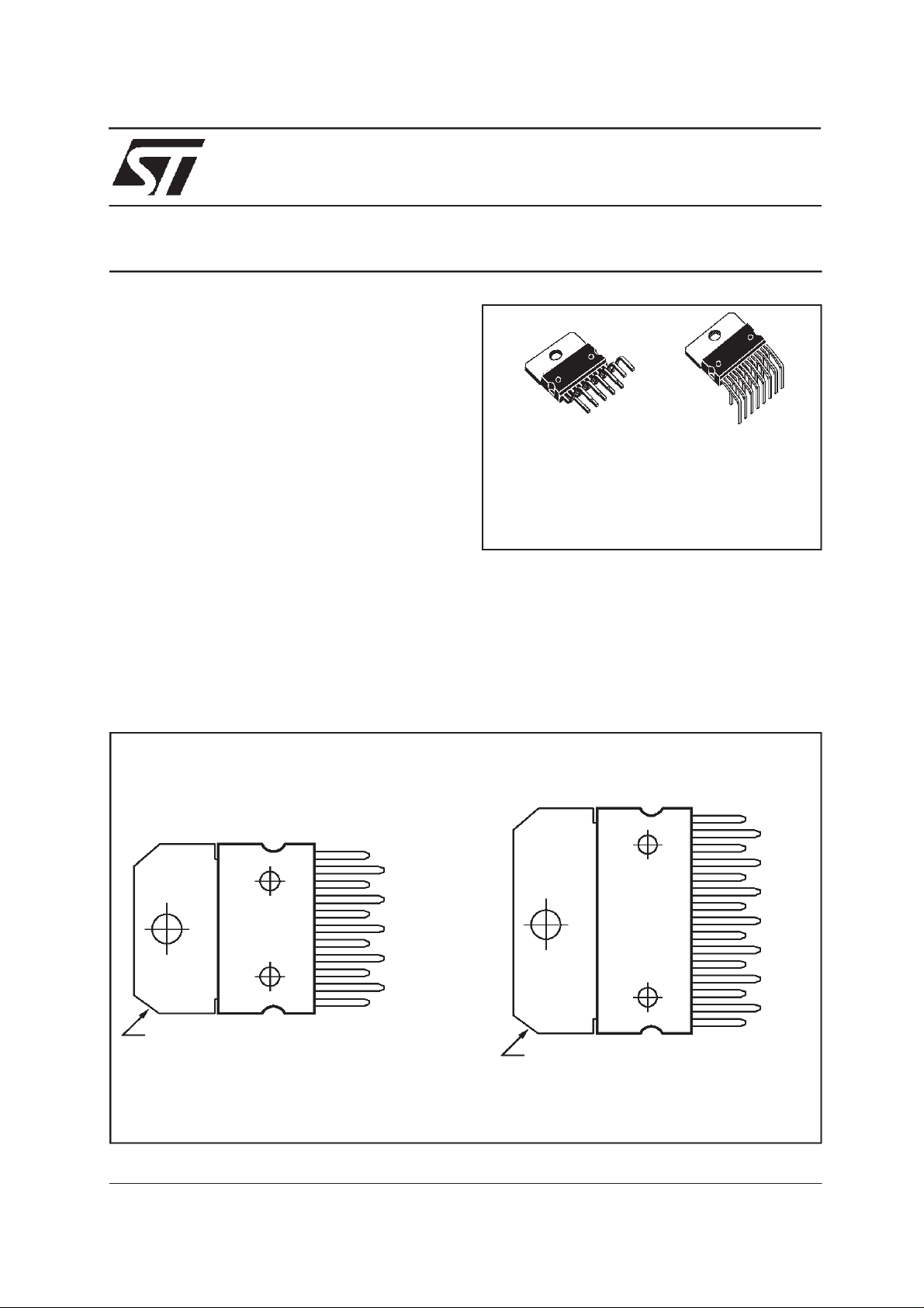
PI N CONNECTION
(top view)
L4936N/NH
Multiwatt11
ORDERINGNUMBERS: L4936N (Multiwatt 11)
DES CRIPTI ON
TheL4936N/NHaremonolithicintegrateddualvoltage regulators with two very low dropout outputs
andadditionalfunctionssuchaspower-onresetand
input voltagesense.They are designedfor supplying microcomputer controlledsystems specially in
automotiveapplications.
Multiwatt15
L4936NH (Multiwatt 15)
June 2000
TAB CONNECTED TOPIN 6
15
14
11
10
9
8
7
6
5
4
3
2
1
D94AT154
OUT2
ADJ
OUT1
SO
RES
GND
EN
CT
N.C.
SI
VS1/VS2
TAB CONNECTED TO PIN 6
13
12
11
10
9
8
7
6
5
4
3
2
1
OUT2
ADJ
OUT1
SO
N.C.
N.C.
RES
GND
EN
N.C.
CT
N.C.
SI
VS1
VS2
D95AT155
1/11
L4936N/NH
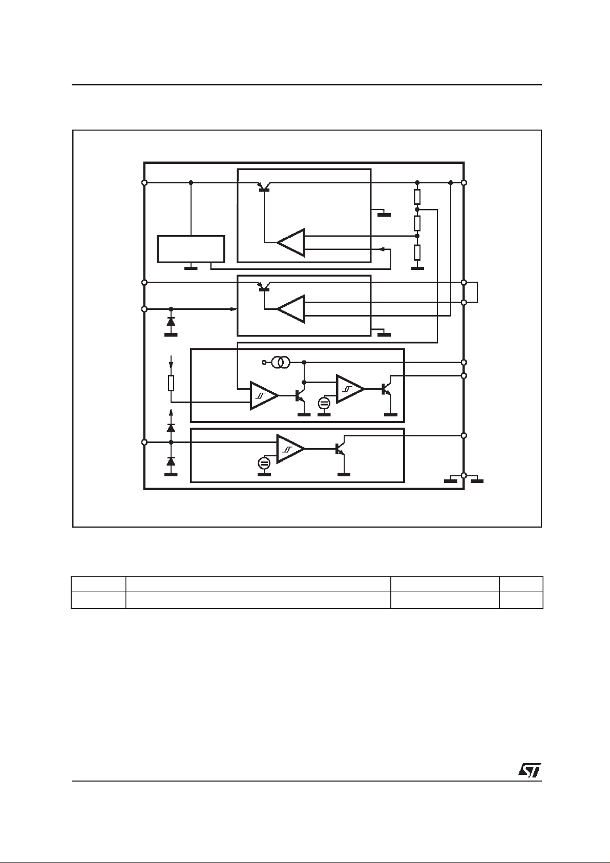
BLOCK DIAG RAM
V
V
EN
S1
REFERENCE
S2
1.23V
RESET
SI
SENSE
(optional)
REG1
REG2
2µ
2.0V
1.23V
1.23V
V
O1
V
O2
ADJ
CT
RES
SO
GND
D94AT143A
THERMAL DATA
Symbol Parameter Value Unit
R
thj-case
Note: VS1, VS2, SI pins are rated at 1500V versus positive ESD according to human body model; other pins are rated at 2000V.
2/11
ThermalResistance Junction-Case Max. 3
C/W
°
L4936N/NH
ABSOLUTE MAXIMUM RATINGS
Symbol Parameter Value Unit
V
T
j,Tstg
I
SI
I
EN
V
EN
V
RES,VSO
I
RES,ISO
P
Note :
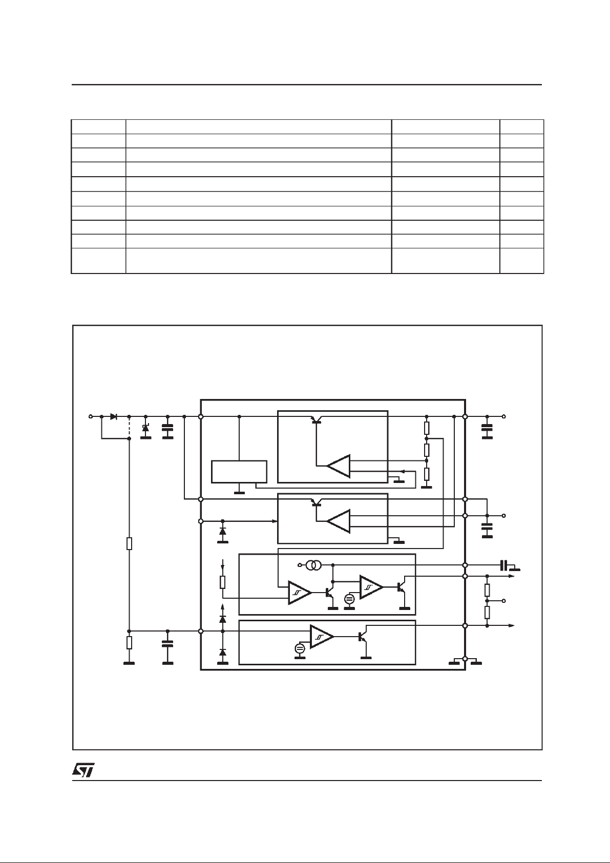
APPLI CATI ON CIRCUI T
DC Supply Voltage 28 V
S
TransientSupply Voltage (T < 1s) 40 V
Junctionand Storage TemperatureRange –55 to 150
Sense Input Current (V
Enable Input Current (VEN≤0.3V)
Enable Input Voltage V
≤
SI
0.3V or V
SI>VS
)
1
±
–1 mA
S
Reset and Sense OutputVoltage 20 V
Reset and Sense OutputCurrent 5 mA
Power Dissipation (TA=80°C, R
D
thheatsink
The circuit is ESD protected according to MIL–STD–883C.
=11°C/W)MW11
POWERDIP
5
1166
C
°
mA
W
mW
V
S1
C
S
REFERENCE
V
S2
EN
1.23V
RESET
SI
SENSE
(optional)
REG1
REG2
2µ
2.0V
1.23V
1.23V
D94AT144A
V
O1
V
O2
ADJ
CT
RES
SO
GND
C
O1
C
O2
CT
R
RES
V
O1
R
SO
CS≥ 1µF;C01≥ 6µF;C02≥ 10µF, ESR < 10Ω at 10KHz
3/11
L4936N/NH
ELECTRICAL CHARACTERISTICS (VS= 14V; –40°C unless otherwise specified)
Symbol Parameter Test Conditions Min. Typ. Max. Unit
V
V
V
O2-VO1
I
ADJ
V
DP1
V
V
DP2
V
V
OL 1.2
V
OLO1
V
OLO2
I
LIM1
I
LIM2
I
QSB
I
Operating Supply Voltage 25 V
S
StandbyOutput Voltage
O1
Output Voltage 2 TrackingError
(note 1)
6V ≤ V
1mA≤I
6V≤V
5mA≤I
≤ 25V
S
O1
≤
S
O2
50mA
≤
25V
500mA
≤
4.90 5.00 5.10 V
–25 +25 mV
Enable= LOW
ADJ InputCurrent IO1= 1mA; IO2= 5mA –1 0.1 1
DropoutVoltage 1 IO1= 10mA
Inputto Output Voltage
IO1
I
= 50mA
O1
VS = 4V,IO1= 35mA 0.4 V
0.1
0.2
Differencein Undervoltage
Condition
DropoutVoltage 2 IO1 = 100mA
Inputto Output Voltage
IO2
I
= 500mA
O1
VS = 4.6V,IO1= 350mA 0.6 V
0.2
0.3
Differencein Undervoltage
Condition
LineRegulation
6V ≤ V
I
Load Regulation 1
Load Regulation 2
1mA≤I
5mA≤I
Current Limit 1 VO1= 4.5V
V
≤ 25V
S
= 1mA; IO2= 5mA
O2
50mA
≤
O1
500mA
≤
O2
= 0V(note 2)
O1
55
25
100
50
Current Limit 2 VO2 = 0V 550 1000 1700 mA
Quiescent Current StandbyMode
(output2 disabled)
Quiescent Current IO1= 50mA
Q
I
= 0.3mA;TJ< 100°C
O1
2.4V
V
≥
EN
V
= 14V
S
V
= 3.5V
S
I
= 500mA
O1
210
340
0.25
0.4
0.3
0.6
20 mV
25 mV
50 mV
200
100
290
850
30 mA
µA
V
V
V
V
mA
mA
µ
µA
A
ENABLE
V
ENL
V
ENH
V
ENhyst
I
EN
4/11
EnableInput LOW Voltage
–0.3 1.5 V
(output2 active)
EnableInput HIGH Voltage 2.4 7 V
EnableHysteresis 30 75 200 mV
EnableInput Current 0V < VEN< 1.2V
2.5V < V
EN
<7V
–10
–1
–1.50–0.5
+1
µ
µ
A
A

L4936N/NH
ELECTRICAL CHARACTERISTICS (continued)
RESET
Symbol Parameter Test Conditions Min. Typ. Max. Unit
V
V
t
RD
t
RR
V
I
LRES
V
CTh
V
CTh, hyst
SENSE
ResetLow Threshold Voltage VS= 14V Vo1-0.4 4.7 Vo1-0.1 V
Rt
ResetThreshold Hysteresis 50 100 200 mV
Rth
ResetPulse Delay
ResetReaction Time CT= 100nF 1 0 50
ResetOutput LOW Voltage
RL
ResetOutput HIGH Leakage V
Delay Comparator Threshold 2.0 V
Delay Comparator Threshold
Hysteresis
= 100nF;tR> 100µs
C
T
= 10KΩto V
R
RES
VS= 1.5V
=5V 1 µ
RES
01
55 100 180 mV
100 mV
0.4 V
µs
A
V
Note :
V
Slth,hyst
V
SOL
I
LSO
Sense Threshold Voltage 1.16 1.23 1.35 V
Slth
Sense Threshold Hysteresis 20 100 200 mV
Sense Output LOW Voltage
Sense Output Leakage
1:V
connected to ADJ.VO2canbe setto higher values by inserting an externalresistor divider.
O2
2 : Foldbackcharacteristic
=0.8V; V
V
SI
R
=10KΩto V
SO
= 5V;VSI≥1.5V
V
SO
FUNCTI O NAL DESCRIPTI ON
TheL4936N/NHarebasedontheSGS-THOMSON
Microelectronics modular voltage regulator approach.Severalout-standingfeaturesandauxiliary
functionsare providedto meet the requirementsof
supplyingthemicroprocessorsystemsusedin automotiveapplications.
Furthermorethe deviceis suitablealso in otherapplicationsrequiringtwostabilizedvoltages.
The modular approach allows other features and
functionsto be realizedeasilywhen required.
STANDBYREGULATOR
The standby regulator uses an Isolated Collector
Vertical PNP transistor as the regulating element.
This structureallowsa verylow dropoutvoltage at
currentsup to 50mA. The dropoutoperationof the
standby regulator is maintained down to 2V input
supply voltage. The output voltage is regulatedup
tothetransientinputsupplyvoltageof40V.Thisfeatureavoids functionalinterruptions whichcould be
generatedby overvoltagepulses.
The typicalcurve of the standbyoutputvoltage as a
functionof theinputsupplyvoltageisshowninfig.1.
3V
≥
S
01
0.4 V
1
µ
The current consumption of the device (quiescent
current) is less than 250µA when output 2 is dis-
abled(standbymode).The dropoutvoltage is controlledto reducethe quiescentcurrentpeak in the
undervoltage region and to improve the transient
responsein this region.
Thequiescentcurrentis showninfig.2asafunction
of the supplyinput voltage2.
OUTPUT2 VOLTAGE
Theoutput2 regulatoruses the sameoutputstruc-
tureas thestandbyregulator,butratedforanoutput
currentof 500mA.
The output2 regulatorworksintrackingmodewith
the standbyoutputvoltage as a referencevoltage
when the output 2 programming pin ADJ is connectedto V
tothe pinADJas shownin fig. 3,the outputvolt-
R
2
. By connectinga resistordividerR1,
O2
age 2 can be programmedto thevalue :
V
O2=VO1
(1 + R1/R2)
The output 2 regulator can be switched off via the
Enableinput.
A
5/11

L4936N/NH
Figure1 : OutputVoltagevs. InputVoltage.
Figure2 : QuiescentCurrent vs. SupplyVoltage.
Figure3 : ProgrammableOutput2 Voltagewith ExternalResistors.
6/11

L4936N/NH
RESETCIRCUIT
Theblockcircuitdiagramoftheresetcircuitisshown
infig.4.Theresetcircuitsupervisesthestandbyoutput voltage. The reset threshold of 4.7Vis defined
by the internal reference voltage and the standby
outputdivider.
The reset pulse delay time t
chargetime of an externalcapacitorC
C
T
=
t
RD
2µA
, is defined by the
RD
x2V
:
T
Thereactiontimeoftheresetcircuitdependsonthe
discharge time limitation of the reset capacitor C
and is proportionalto the value of CT.
The reaction time of the reset circuitincreasesthe
noiseimmunity.In fact,ifthestandbyoutputvoltage
Figure4 :Block Diagramof the ResetCircuit.
drops below the reset thresholdfor a time shorter
thanthe reactiontimet
, noresetoutputvariation
RR
occurs. The nominal reset delay is generated for
standbyoutput voltage drops longer than the time
necessary for the complete discharging of the capacitorC
C
T
. This time is typically equal to 50µsif
T
=100nF.Thetypicalresetoutputwaveformsare
shownin fig.5.
SENSECOMPARATOR
Thiscircuitcomparesaninputsignalwithan internal
voltagereferenceof typically1.23V.The useof an
externalvoltagedividermakesthecomparatorvery
flexiblein theapplication.Thisfunctioncanbeused
tosupervisetheinputvoltage-eitherbeforeor after
T
theprotectiondiode- andtogiveadditionalinformationtothemicroprocessorsuchaslowvoltagewarnings.
7/11

L4936N/NH
Figure5 : TypicalResetOutputWaveforms.
1.5V
8/11

L4936N/NH
DIM.
MIN. TYP. MAX. MIN. TYP. MAX.
A5
B 2.65 0.104
C 1.6 0.063
D 1 0.039
E 0.49 0.55 0.019 0.022
F 0.88 0.95 0.035 0.037
G 1.45 1.7 1.95 0.057 0.067 0.077
G1 16.75 17 17.25 0.659 0.669 0.679
H1 19.6 0.772
H2 20.2 0.795
L 21.9 22.2 22.5 0.862 0.874 0.886
L1 21.7 22.1 22.5 0.854 0.87 0.886
L2 17.4 18.1 0.685
L3 17.25 17.5 17.75 0.679 0.689 0.699
L4 10.3 10.7 10.9 0.406 0.421 0.429
L7 2.65 2.9 0.104 0.114
M 4.25 4.55 4.85 0.167 0.179 0.191
M1 4.73 5.08 5.43 0.186 0.200 0.214
S 1.9 2.6 0.075 0.102
S1 1.9 2.6 0.075 0.102
Dia1 3.65 3.85 0.144 0.152
mm inch
0.197
0.713
OUTLINE AND
MECHANICAL DATA
Multiwatt11 V
9/11

L4936N/NH
DIM.
MIN. TYP. MAX. MIN. TYP. MAX.
A5
B 2.65 0.104
C 1.6 0.063
E 0.49 0.55 0.019 0.022
F 0.66 0.75 0.026 0.030
G 1.14 1.27 1.4 0.045 0.050 0.055
G1 17.57 17.78 17.91 0.692 0.700 0.705
H1 19.6 0.772
H2 20.2 0.795
L 20.57 0.810
L1 18.03
L2 2.54
L3 17.25 17.5 17.75 0.679 0.689
L4 10.3 10.7 10.9 0.406 0.421 0.429
L5 5.28 0.208
L6 2.38
L7 2.65 2.9 0.104 0.114
S 1.9 2.6 0.075 0.102
S1 1.9 2.6 0.075 0.102
Dia1 3.65 3.85 0.144 0.152
mm inch
0.197
0.710
0.100
0.699
0.094
OUTLINE AND
MECHANICAL DATA
Multiwatt15 H
10/11

L4936N/NH
Information furnished is believed to be accurate and reliable. However, STMicroelectronics assumes no responsibility for the consequences of use of such information nor for any infringement of patents or other rights of third parties which may result from its use. No
license is granted by implication or otherwise under any patent or patent rights of STMicroelectronics. Specification mentioned in this
publication are subject to change without notice. This publication supersedes and replaces all information previously supplied. STMicroelectronics products are not authorized for use as critical components in life support devices or systems without express written
approval of STMicroelectronics.
Australia - Brazil - China - Finland - France - Germany - Hong Kong - India - Italy - Japan - Malaysia - Malta - Morocco -
The ST logo is a registered trademark of STMicroelectronics
2000 STMicroelectronics – Printedin Italy – All Rights Reserved
MULTIWATTis a Registered Trademark of STMicroelectronics
STMicroelectronics GROUP OF COMPANIES
Singapore - Spain - Sweden - Switzerland - United Kingdom - U.S.A.
http://www.st.com
11/11
 Loading...