

ADVANCEDVOLTAGE REGULATOR
ENABLE AND SENSE INPUTS (EN, SI) PROTECTED AGAINST NEGATIVE TRANSIENTS
DOWN TO-5V
RESET THRESHOLD ADJUSTABLE FROM
3.8 TO 4.7V
EXTREMELY LOW QUIESCENT CURRENT,
65µA (LESS THAN 90µA) IN STANDBY
MODE
OPERATINGDC SUPPLY VOLTAGE RANGE
5V -28V
OPERATING TRANSIENT SUPPLY VOLTAGE UP TO 40V
HIGHPRECISIONSTANDBYOUTPUTVOLTAGE 5V±1% WITH 100mA CURRENT CAPABILITY
OUTPUT 2 VOLTAGE 5V ± 2% WITH 400mA
CURRENT CAPABILITY (ADJ WIRED TO
V
)
OUT2
OUTPUT 2 VOLTAGE ADJUSTABLE BY EXTERNAL VOLTAGEDIVIDER
OUTPUT 2 DISABLE FUNCTION FOR
STANDBYMODE
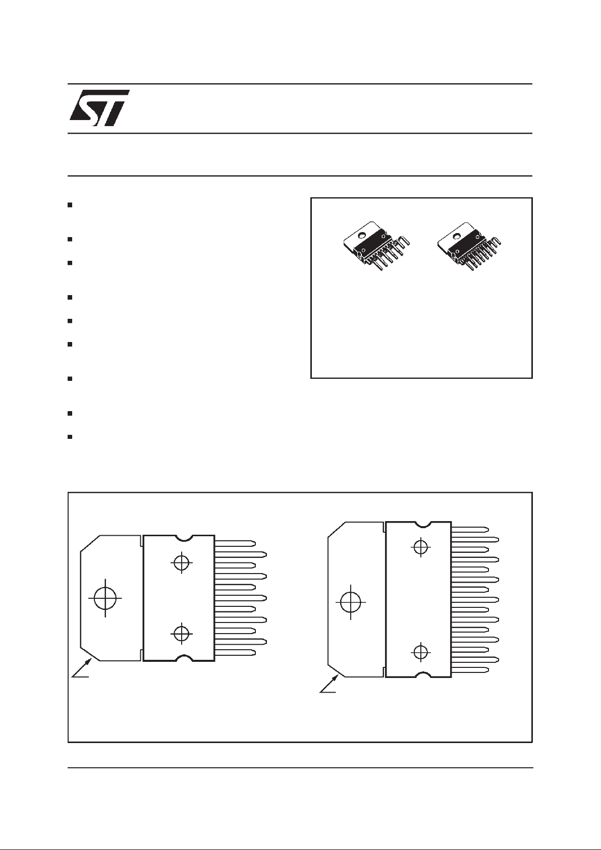
L4936E
MULTIWATT 11
ORDERING NUMBERS: L4936E (Multiwatt 11)
DESCRIPTION
The L4936E is a monolithic integrated dual voltage regulator with two very low dropout outputs
and additionalfunctionsas power-on resetand input voltage sense.It is designedfor supplyingthe
microcomputer controlled systems especially in
automotiveapplications.
MULTIWATT 15
L4936EH (Multiwatt15)
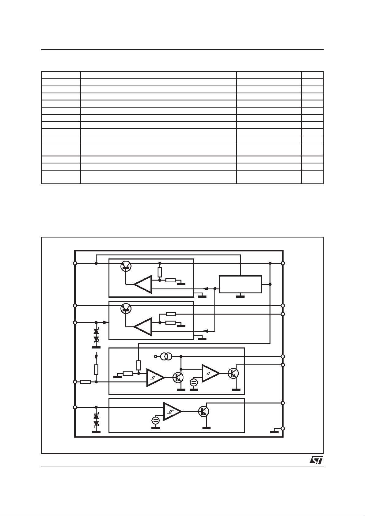
PIN CONNECTIONS (Top views)
11
10
9
8
7
6
5
4
3
2
1
TAB CONNECTEDTO PIN 6
Multiwatt11
June 2000
D94AT077
OUT2
ADJ
OUT1
SO
RES
GND
EN
CT
PR
SI
VS1/VS2
TAB CONNECTEDTO PIN 6
Multiwatt15
15
14
13
12
11
10
9
8
7
6
5
4
3
2
1
D94AT078A
OUT2
ADJ
OUT1
SO
N.C.
N.C.
RES
GND
EN
N.C.
CT
PR
SI
VS1
VS2
1/11
L4936E
ABSOLUTE MAXIMUM RATINGS
Symbol Parameter Value Unit
V
INDC
V
INTR
I
O
V
SI
I
SI
V
EN
I
EN
V
RES,VSO
I
RES,ISO
P
O
T
stg
T
j
T
JSD
Note: The circuit is ESD protected according to MIL-STD-883C
Note 2: Current forced means voltage unlimited but current limited to thespecified value
Voltageforced meansvoltage limited to the specified valueswhile the current is not limited
Note 3: Typicalvalue soldered on a PCboard with 8 cm2 copper ground plane (35mm thick)
DC Operating Supply Voltage 28 V
Transient Operating Supply Voltage (T < 400ms) -14 to 40 V
Output Current internally limited
Sense Input Voltage (VoltageForced) (note 2) -20 to 20 V
Sense Input Current (Current Forced) (note 2) ±1mA
Enable Input Voltage(Voltage Forced) (note 2) -20 to 20 V
Sense Input Current (Current Forced) (note 2)
1mA
±
Output Voltages -0.3 to 20 V
Output Currents (Output Low) 5 mA
Power Dissipation at T
Multiwatt 11 (R
heatsink = 9K/W)
th
=80°C (note 3)
amb
5W
Storage Temperature -65 to 150
Operating Junction Temperature -40 to 150
Thermal shutdownjunction temperature Output 2 will shut-down
165 °C
typically at Tj 10K lowerthan output 1
C
°
C
°
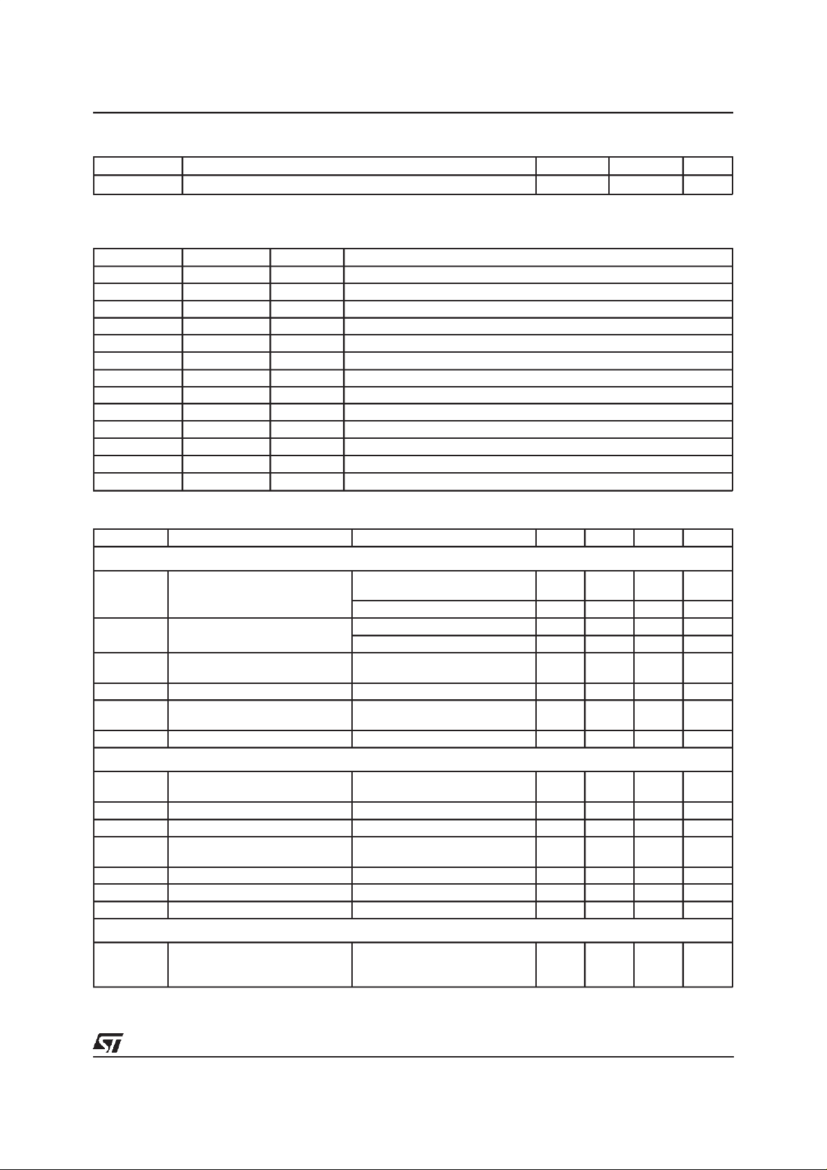
BLOCK DIAGRAM
VS1
VS2
EN
1.23V
PR
SI
REG1
REG2
RESET
OUT1
1.23V REFERENCE
OUT2
ADJ
1.23V
CT
RES
1.4V
SO
2/11
SENSE
1.23V
GND
D94AT074A
THERMAL DATA
Symbol Parameter MW 11 MW 15 Unit
R
th j-case
Note 3: Typicalvalue soldered on a PCboard with 8 cm2 copper ground plane (35mm thick)
Thermal ResistanceJunction-case 3
PIN FUNCTIONS
PIN (MW 11) PIN (MW 15) Name Function
1 1 VS1 Supply Voltage(400mA Regulator)
1 2 VS2 Supply Voltage(100mA Regulator, Reset, Sense)
2 3 S1 Sense Input
3 4 PR Reset Theresold Programming
4 5 CT Reset Delay Capacitor
5 7 EN Enable (low will activate the 400mAregulator)
6 8 GND Ground
7 9 RES Reset Output
8 12 SO Sense Output
9 13 OUT 1 100mA RegulatorOutput
10 14 ADJ Feedback of 400mA Regulator
11 15 OUT 2 400mA RegulatorOutput
6, 10, 11 NC Not Connected
L4936E
C/W
°
ELECTRICALCHARACTERISTICS
= 14V; Tj=-40 to 150°C unless otherwise specified.)
(V
S
Symbol Parameter Test Condition Min. Typ. Max. Unit
OUT 1
V
V
V
V
OL01
I
QSB
O1
DP1
LIM1
Supply Output Voltage VS= 6 to 28V;
I
= 400µA to 100mA
O1
T
125°C; I
≤
Dropoutput Voltage 1 I
Load Regulation 1 I
j
OUT1
I
OUT1
OUT1
O1
= 10mA 0.1 0.2 V
= 100mA; VS= 4.8V 0.2 0.4 V
= 1 to 100mA
= 50 to 400µA 4.8 5 5.2 V
4.9 5 5.1 V
25 mV
(after regulation setting)
Current Limit 1 VOUT1 = 0.8 to 4.5V 100 200 400 mA
Quiescent Current in Standby
Mode
2.4V (output 2 disabled)
I
≥
EN
I
= 0.1mA; VSI> 1.3V
O1
T
<85°C;RPR=0 75 µA
J
65 90
OUT 2
V
V
R
V
OL02
I
LIM2
O2
DP2
ADJ
I
Q
Output Voltage 2
ADJ connected to OUT 2
Dropoutput Voltage 2 I
Load Regulation 2 I
Enable = LOW;VS= 6 to 28V;
I
= 5 to 400mA
02
= 100mA; VS= 4.8V 0.2 0.3 V
OUT2
I
= 400mA; VS= 4.8V 0.3 0.6 V
OUT2
= 5 to 400mA
OUT1
4.9 5.1 V
50 mV
(after regulation setting)
Adjust Input Resistance 60 100 150 K
Current Limit 2 V02 = 0.8 to 4.5V 450 650 1300 mA
Quiescent Current I
OUT1
= 100mA; I
= 400mA 20 mA
OUT2
OUT1,OUT 2
V
OLi 1,2
Line Regulation VS= 6 to 28V; IO1= 1mA,
I
= 5mA,
O2
(after regulation setting)
20 mV
A
µ
Ω
3/11
L4936E
ELECTRICALCHARACTERISTICS (Continued.)
Symbol Parameter Test Condition Min. Typ. Max. Unit
ENABLE INPUT
V
ENL
V
ENH
V
ENhyst
I
EN LOW
I
EN HIGH
RESETCIRCUIT
V
RT
V
RTH
t
RD min
t
RD nom
t
RR
I
CT
I
CT
V
RESL
V
RESH
Enable Input Low Voltage
-20 1 V
(Output 2 Active)
Enable Input High Voltage 1.4 20 V
Enable Hysteresis 20 30 60 mV
Enable Input Current Low VEN= 0 -20 -8 -3
Enable Input Current High VEN= 1.1 to 7V; TJ< 130°C; -1 0 1
= 1.1 to 7V;
V
EN
T
= 130 to 150°C;
J
Reset Theresold Voltage
(note4)
RPR=
R
PR
Reset Theresold Hysteresis RPR=
Reset Pulse Delay C
Reset Pulse Delay C
Reset Reaction Time C
Pull Down Capability of the
RES
RES
RES
V
OUT1<VRT
∞
= 0 3.65 3.8 3.95 V
∞
= 47nF; tr≤ 30µs; (note 5) 40 60 100 ms
= 47nF; (note 6) 60 100 140 ms
= 47nF 10 50 150
-10 0 10 µA
4.5 VO1-0.3 VO1-0.2 V
15 40 100 mV
3615mA
Discharge circuit
Charge Current VOUT1 >VRT -1.3 -1 0.7 µA
Reset Output Low Voltage RRES = 10KΩ to VOUT1
1.5V
OUT1 ≥
=5V 1
RES
Reset Output High Leakage
V
V
0.4 V
current
A
µ
A
µ
s
µ
A
µ
SENSECOMPARATOR
V
SI
V
SIT
V
SITH
V
SOL
I
SOH
I
SI HIGH
I
SI LOW
Note :
4) The reset threshold can beprogrammed continuously from typ 3.8V to 4.7V by changing a valueof an external resistor frompin PR to GN
5) This is a minimum reset timeaccording to the hysteresis of the comparator.Delay time starts with V
6) This is thenominal reset time depending on thedischarging limit of CT(saturationvoltage) and theupper threshold of the timer comparator.
Delay time starts with V
7) The leakage of CTmust be less than 0.5mA (2V). Ifan externalresistor between CT and VOUT1is applied, the leakage current may be
increased. The external resistor should have more than 30KΩ.
for stability: Cs ≥ 1µF, C01 ≥ 10µF, C02 ≥ 10µF, ESR ≤ 5Ω (designed targetfor resistive load) For details see applicationnote.
8) For transients exceeding 20V or -20V externalprotection is required at thePins SIand EN as shown at Pin EN. The protectionproposed will
provide proper function for transients in the range of±200V. If the zener diode is omitted the external resistor should be raised to200K
to limit the current to 1mA. Withoutthe zener diode, the function 20V or -20V can not be guaran teed.
Functional Range -20 20 V
Sense Threshold Voltage Falling Edge; TJ<130°C 1.08 1.16 1.24 V
Falling Edge; T
130 to 150°C 1.05 1.16 1.29 V
J
Sense Threshold Hysteresis 10 30 60 mV
Sense Output Low Voltage V
Sense Output Leakage VSO= 5V; V
Sense Input Current High VSI= 1.1 to 7V; TJ<130°C-101
1.05V; R
≤
SI
connected to 5V; V
= 1.1to 7V; TJ130 to 150°C -10 0 10
V
SI
=10K
SO
SI ≥
Ω
S ≥ 5V
1.5V 1
0.4 V
µ
µ
µ
Sense Input Current Low VSI = 0V -20 -8 -3 µA
OUT1 exceeding VRT
OUT1 exceeding VRT
A
A
A
Ω
4/11
 Loading...