

SGS Thomson Microelectronics L4931CZ80, L4931CZ60, L4931CV40, L4931CV35, L4931CV33 Datasheet
...
L4931
SERIES
VERY LOW DROP
VOLTAGE REGULATORS WITH INHIBIT
April 1999
■ VERYLOW DROPOUTVOLTAGE(0.4V)
■ VERYLOW QUIESCENTCURRENT
(TYP. 50 µA IN OFF MODE, 600µAINON
MODE)
■ OUTPUTCURRENT UP TO 250 mA
■ LOGIC-CONTROLLEDELECTRONIC
SHUTDOWN
■ OUTPUTVOLTAGESOF 1.25;1.5; 2.5;2.7;
3; 3.3;3.5; 4; 4.5; 4.7; 5; 5.2; 5.5; 6; 8; 12V
■ INTERNALCURRENT AND THERMALLIMIT
■ ONLY2.2µF FOR STABILITY
■ AVAILABLEIN ± 1% (AB) OR 2% (C)
SELECTIONAT 25
o
C
■ SUPPLYVOLTAGEREJECTION:
70db TYP. FOR 5V VERSION
■ TEMPERATURERANGE: -40 TO 125
o
C
DESCRIPTION
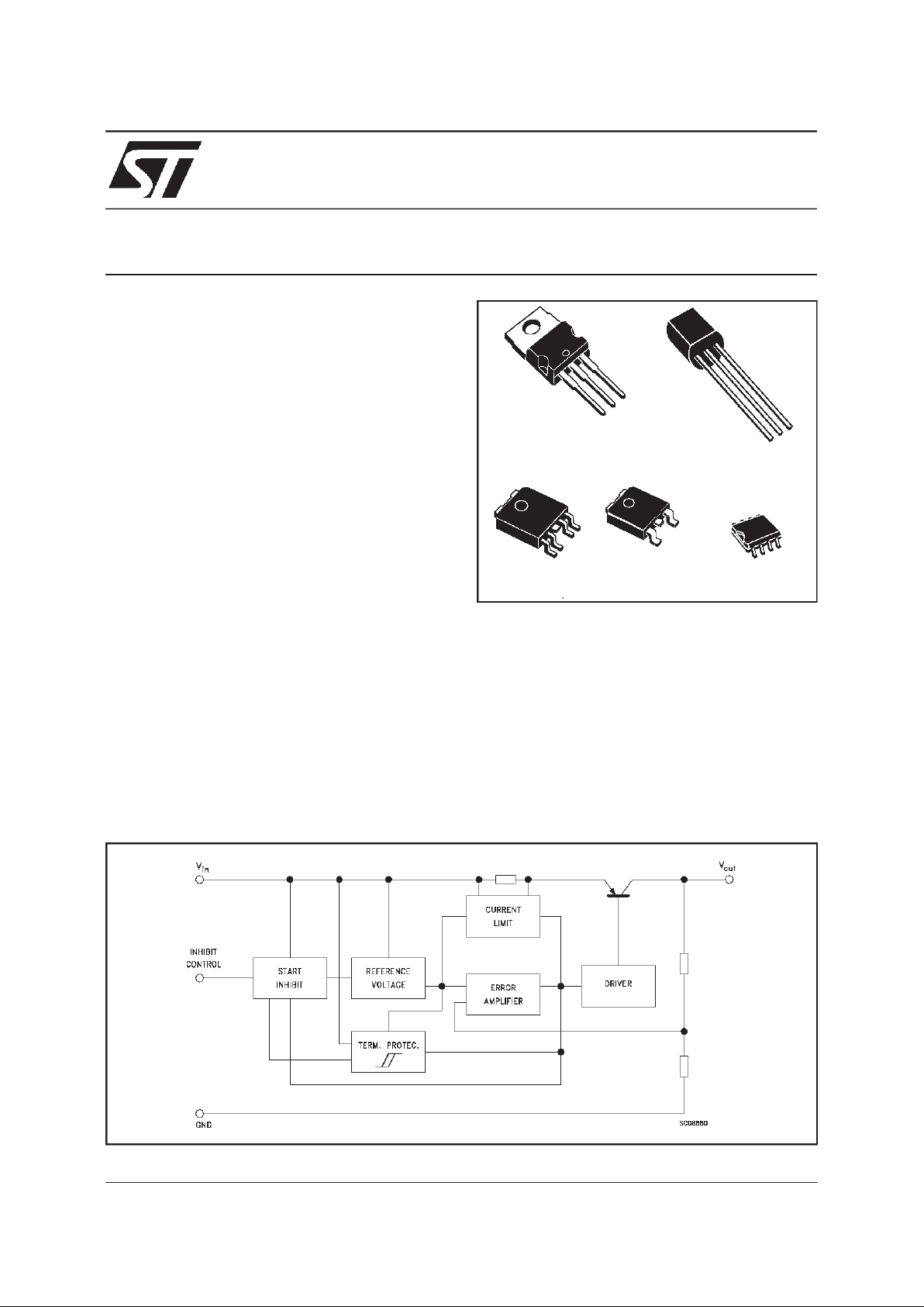
The L4931 series are very Low Drop regulators
available in TO-220, SO-8, DPAK, PPAK and
TO-92 packages and in a wide range of output
voltages.
The very Low Drop voltage (0.4V) and the very
low quiescent current make them particularly
suitable for Low Noise, Low Power applications
and specially in batterypoweredsystems.
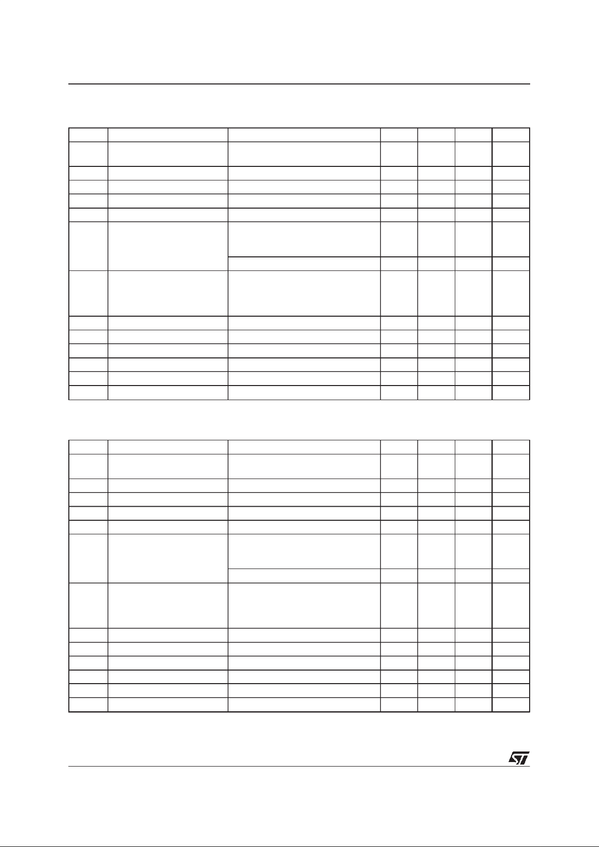
In PPAK and SO-8 packages a Shutdown Logic
Control function is available TTL compatible. This
means that when the device is used as a local
regulator,it is possible to put a part of the board
in standby, decreasing the total power
consumption. It requires only a 2.2 µF capacitor
for stability allowing space and cost saving.
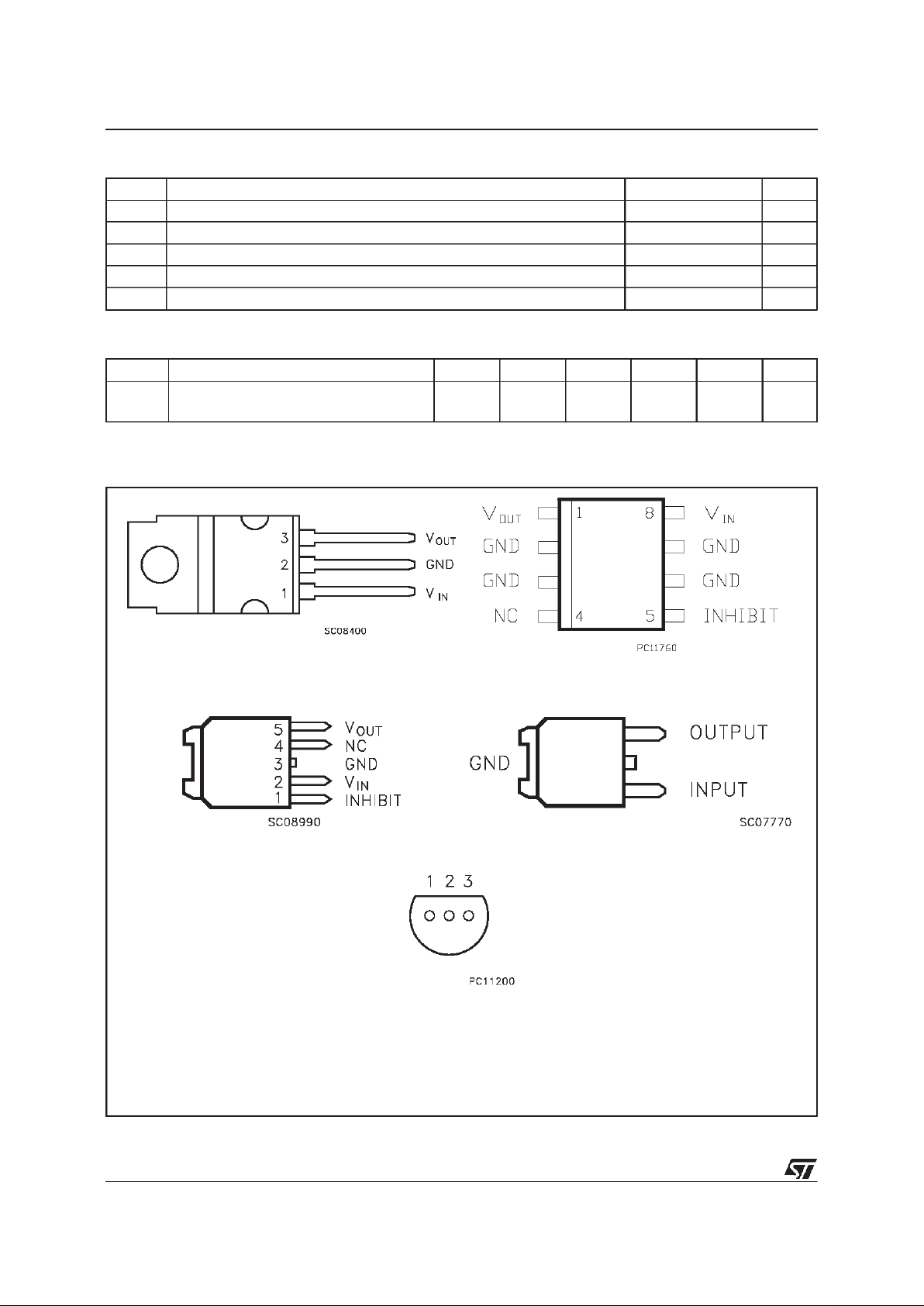
SCHEMATIC DIAGRAM
PPAK
1
3
DPAK
TO-220
SO-8
TO-92
1/25
ABSOLUTE MAXIMUM RATINGS
Symb ol Parameter Value Unit
V
i
DC Input Voltage 20 V
I
o
Output Current Internally limited
P
tot
Power Dissipation Internally limited
T
stg
Storage Temperature Range - 40 to 150
o
C
T
op
Operating Junction Temperature Range - 40 to 125
o
C
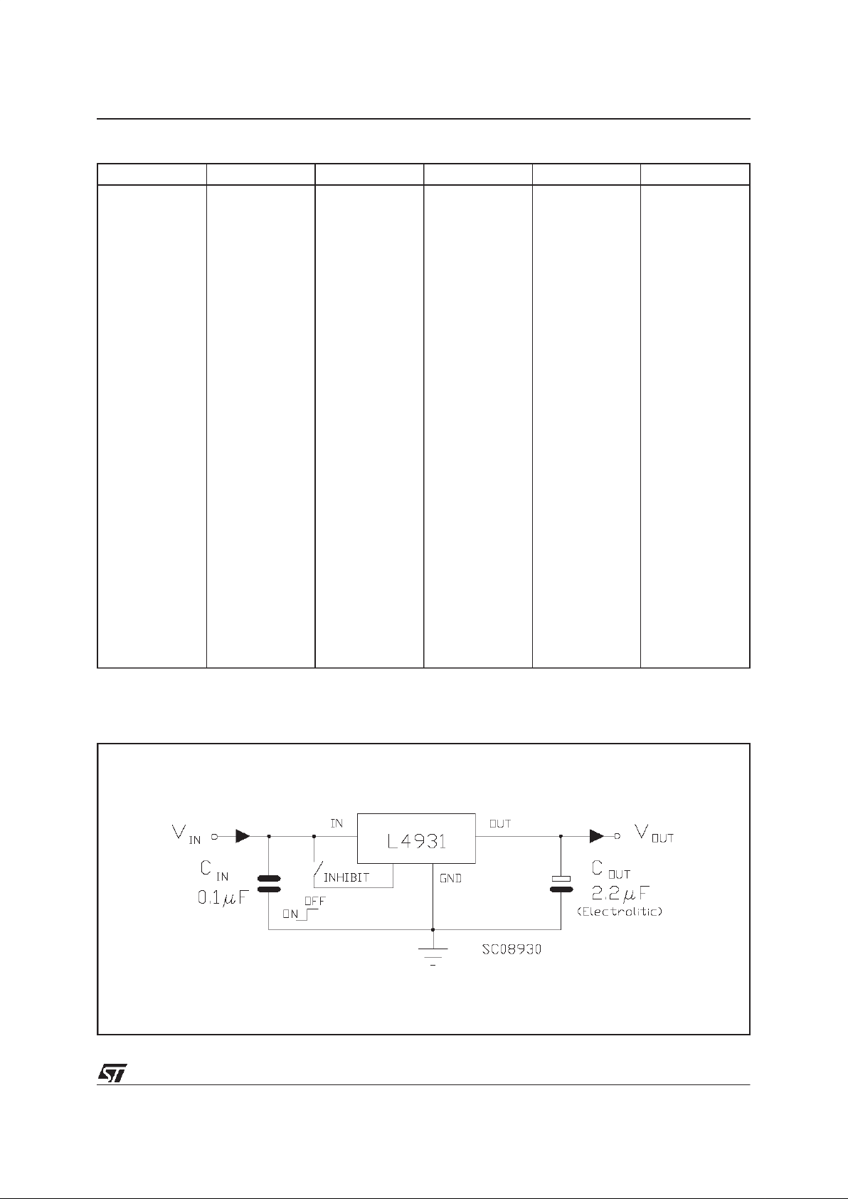
CONNECTION DIAGRAM
(top view)
THERMALDATA
Symbo l Parameter TO-220 SO-8 DPAK PP AK TO-92 Unit
R
thj-cas e
R
thj-amb
Thermal Resistance Junction-case
Thermal Resistance Junction-ambient
3
50
20
55(*)
8
100
8
100 200
o
C/W
o
C/W
(*) Considering 6 cm2of copper board heat-sink
TO-220 SO-8
PPAK DPAK
TO-92
pin 1 = V
OUT
pin 2 = GND
pin 3 = V
IN
BOTTOM VIEW
L4931 SERIES
2/25
ORDERING NUMBERS
TO-220 SO-8 PPAK DPAK T O-92 Output Voltage
L4931CV12 (*)
L4931ABV12 (*)
L4931CV15 (*)
L4931ABV15 (*)
L4931CV25 (*)
L4931ABV25 (*)
L4931CV27
L4931ABV27
L4931CV30
L4931ABV30
L4931CV33
L4931ABV33
L4931CV35
L4931ABV35
L4931CV40
L4931ABV40
L4931CV45 (*)
L4931ABV45 (*)
L4931CV47
L4931ABV47
L4931CV50
L4931ABV50
L4931CV52 (*)
L4931ABV52 (*)
L4931CV55 (*)
L4931ABV55 (*)
L4931CV60
L4931ABV60
L4931CV80
L4931ABV80
L4931CV120
L4931ABV120
L4931CD12 (*)
L4931ABD12 (*)
L4931CD15 (*)
L4931ABD15 (*)
L4931CD25 (*)
L4931ABD25 (*)
L4931CD27
L4931ABD27
L4931CD30
L4931ABD30
L4931CD33
L4931ABD33
L4931CD35
L4931ABD35
L4931CD40
L4931ABD40
L4931CD45 (*)
L4931ABD45 (*)
L4931CD47
L4931ABD47
L4931CD50
L4931ABD50
L4931CD52 (*)
L4931ABD52 (*)
L4931CD55 (*)
L4931ABD55 (*)
L4931CD60
L4931ABD60
L4931CD80
L4931ABD80
L4931CD120
L4931ABD120
L4931CPT12 (*)
L4931ABPT12 (*)
L4931CPT15 (*)
L4931ABPT15 (*)
L4931CPT25 (*)
L4931ABPT25 (*)
L4931CPT27
L4931ABPT27
L4931CPT30
L4931ABPT30
L4931CPT33
L4931ABT33
L4931CPT35
L4931ABPT35
L4931CPT40
L4931ABPT40
L4931CPT45 (*)
L4931ABPT45 (*)
L4931CPT47
L4931ABPT47
L4931CPT50
L4931ABPT50
L4931CPT52 (*)
L4931ABPT52 (*)
L4931CPT55 (*)
L4931ABPT55 (*)
L4931CPT60
L4931ABPT60
L4931CPT80
L4931ABPT80
L4931CPT120
L4931ABPT120
L4931CDT12 (*)
L4931ABDT12 (*)
L4931CDT15 (*)
L4931ABDT15 (*)
L4931CDT25 (*)
L4931ABDT25 (*)
L4931CDT27
L4931ABDT27
L4931CDT30
L4931ABDT30
L4931CDT33
L4931ABDT33
L4931CDT35
L4931ABDT35
L4931CDT40
L4931ABDT40
L4931CDT45 (*)
L4931ABDT45 (*)
L4931CDT47
L4931ABDT47
L4931CDT50
L4931ABDT50
L4931CDT52 (*)
L4931ABDT52 (*)
L4931CDT55 (*)
L4931ABDT55 (*)
L4931CDT60
L4931ABDT60
L4931CDT80
L4931ABDT80
L4931CDT120
L4931ABDT120
L4931CZ12 (*)
L4931ABZ12 (*)
L4931CZ15 (*)
L4931ABZ15 (*)
L4931CZ25 (*)
L4931ABZ25 (*)
L4931CZ27
L4931ABZ27
L4931CZ30
L4931ABZ30
L4931CZ33
L4931ABZ33
L4931CZ35
L4931ABZ35
L4931CZ40
L4931ABZ40
L4931CZ45 (*)
L4931ABZ45 (*)
L4931CZ47
L4931ABZ47
L4931CZ50
L4931ABZ50
L4931CZ52 (*)
L4931ABZ52 (*)
L4931CZ55 (*)
L4931ABZ55 (*)
L4931CZ60
L4931ABZ60
L4931CZ80
L4931ABZ80
L4931CZ120
L4931ABZ120
1.25 V
1.25 V
1.5 V
1.5 V
2.5 V
2.5 V
2.7 V
2.7 V
3V
3V
3.3 V
3.3 V
3.5 V
3.5 V
4V
4V
4.5 V
4.5 V
4.75 V
4.75 V
5V
5V
5.2 V
5.2 V
5.5 V
5.5 V
6V
6V
8V
8V
12 V
12 V
(*) Available on request
TESTCIRCUITS
L4931 SERIES
3/25
ELECTRICALCHARACTERISTICS FOR L4931ABxx12(refer to the test circuits, Tj=25oC,
C
i
= 0.1 µF, Co= 2.2 µF unless otherwise specified)
Symbol Parameter Test Cond itions Min. Typ. M ax. Unit
V
o
Output Voltage Io=5mA,Vi=3.3V
I
o
=5mA,Vi= 3.3 V -25<Ta<85oC
1.238
1.225
1.25 1.263
1.275
V
V
V
i
Operating Input Voltage Io=250mA 2.5 20 V
I
out
Output Current Limit 300 mA
∆V
o
Line Regulation Vi= 2.5 to 20 V, Io=0.5mA 3 15 mV
∆V
o
(*) Load Regulation Vi=2.7V Io= 0.5 to 250 mA 3 15 mV
I
d
Quiescent Current ON MODE
V
i
= 2.7 to 20 V Io=0mA
V
i
= 2.7 to 20 V Io= 250 mA
0.6
4
1
6
mA
mA
OFFMODE V
i
=6V 50 100
µ
A
SVR Supply Voltage Rejection
I
o
=5mA Vi=3.7V±1V
f = 120 Hz
f=1KHz
f = 10 KHz
80
77
55
dB
dB
dB
eN Output Noise Voltage B = 10 Hz to 100 KHz 50
µ
V
V
d
(*) Dropout Voltage Io= 250 mA 1.25 V
V
il
Control Input Logic Low -40 < Ta<125oC0.8V
V
ih
Control Input Logic High -40 < Ta<125oC2 V
I
i
Control Input Current Vi= 6 V, Vc=6V 10
µ
A
C
O
Output Bypass Capacitance
ESR = 0.1 to 10ΩI
o
= 0 to 250 mA
210
µ
F
ELECTRICALCHARACTERISTICS FOR L4931Cxx12(refer to the testcircuits, Tj=25oC,
C
i
= 0.1 µF, Co= 2.2 µF unless otherwise specified)
Symbol Parameter Test Cond itions Min. Typ. M ax. Unit
V
o
Output Voltage Io=5mA,Vi=3.3V
I
o
=5mA,Vi= 3.3 V -25<Ta<85oC
1.225
1.2
1.25 1.275
1.3
V
V
V
i
Operating Input Voltage Io=250mA 2.5 20 V
I
out
Output Current Limit 300 mA
∆
V
o
Line Regulation Vi= 2.5 to 20 V, Io=0.5mA 3 18 mV
∆
V
o
(*) Load Regulation Vi=2.7V Io= 0.5 to 250 mA 3 18 mV
I
d
Quiescent Current ON MODE
V
i
= 2.7 to 20 V Io=0mA
V
i
= 2.7 to 20 V Io= 250 mA
0.6
4
1
6
mA
mA
OFFMODE V
i
=6V 50 100 µA
SVR Supply Voltage Rejection
I
o
=5mA Vi=3.7V±1V
f = 120 Hz
f=1KHz
f = 10 KHz
80
77
55
dB
dB
dB
eN Output Noise Voltage B = 10 Hz to 100 KHz 50 µV
V
d
(*) Dropout Voltage Io= 250 mA 1.25 V
V
il
Control Input Logic Low -40 < Ta<125oC0.8V
V
ih
Control Input Logic High -40 < Ta<125oC2 V
I
i
Control Input Current Vi= 6 V, Vc=6V 10
µ
A
C
O
Output Bypass Capacitance
ESR = 0.1 to 10ΩI
o
= 0 to 250 mA
210 µF
(*) For SO-8 package the maximum limit of load regulationand dropout is increased by 20mV
L4931 SERIES
4/25
ELECTRICALCHARACTERISTICS FOR L4931ABxx15(refer to the test circuits, Tj=25oC,
C
i
= 0.1 µF, Co= 2.2 µF unless otherwise specified)
Symbol Parameter Test Cond itions Min. Typ. M ax. Unit
V
o
Output Voltage Io=5mA,Vi=3.5V
I
o
=5mA,Vi= 3.5 V -25<Ta<85oC
1.485
1.47
1.5 1.515
1.53
V
V
V
i
Operating Input Voltage Io=250mA 2.5 20 V
I
out
Output Current Limit 300 mA
∆V
o
Line Regulation Vi= 2.5 to 20 V, Io=0.5mA 3 15 mV
∆V
o
(*) Load Regulation Vi=2.7V Io= 0.5 to 250 mA 3 15 mV
I
d
Quiescent Current ON MODE
V
i
= 2.7 to 20 V Io=0mA
V
i
= 2.7 to 20 V Io= 250 mA
0.6
4
1
6
mA
mA
OFFMODE V
i
=6V 50 100
µ
A
SVR Supply Voltage Rejection
I
o
=5mA Vi=3.7V±1V
f = 120 Hz
f=1KHz
f = 10 KHz
79
76
55
dB
dB
dB
eN Output Noise Voltage B = 10 Hz to 100 KHz 50
µ
V
V
d
(*) Dropout Voltage Io=250mA 1 V
V
il
Control Input Logic Low -40 < Ta<125oC0.8V
V
ih
Control Input Logic High -40 < Ta<125oC2 V
I
i
Control Input Current Vi= 6 V, Vc=6V 10
µ
A
C
O
Output Bypass Capacitance
ESR = 0.1 to 10ΩI
o
= 0 to 250 mA
210
µ
F
ELECTRICALCHARACTERISTICS FOR L4931Cxx15(refer to the testcircuits, Tj=25oC,
C
i
= 0.1 µF, Co= 2.2 µF unless otherwise specified)
Symbol Parameter Test Cond itions Min. Typ. M ax. Unit
V
o
Output Voltage Io=5mA,Vi=3.5V
I
o
=5mA,Vi= 3.5 V -25<Ta<85oC
1.47
1.44
1.5 1.53
1.56
V
V
V
i
Operating Input Voltage Io=250mA 2.5 20 V
I
out
Output Current Limit 300 mA
∆
V
o
Line Regulation Vi= 2.5 to 20 V, Io=0.5mA 3 18 mV
∆
V
o
(*) Load Regulation Vi=2.7V Io= 0.5 to 250 mA 3 18 mV
I
d
Quiescent Current ON MODE
V
i
= 2.7 to 20 V Io=0mA
V
i
= 2.7 to 20 V Io= 250 mA
0.6
4
1
6
mA
mA
OFFMODE V
i
=6V 50 100 µA
SVR Supply Voltage Rejection
I
o
=5mA Vi=3.7V±1V
f = 120 Hz
f=1KHz
f = 10 KHz
79
76
55
dB
dB
dB
eN Output Noise Voltage B = 10 Hz to 100 KHz 50 µV
V
d
(*) Dropout Voltage Io=250mA 1 V
V
il
Control Input Logic Low -40 < Ta<125oC0.8V
V
ih
Control Input Logic High -40 < Ta<125oC2 V
I
i
Control Input Current Vi= 6 V, Vc=6V 10
µ
A
C
O
Output Bypass Capacitance
ESR = 0.1 to 10ΩI
o
= 0 to 250 mA
210 µF
(*) For SO-8 package the maximum limit of load regulationand dropout is increased by 20mV
L4931 SERIES
5/25

ELECTRICALCHARACTERISTICS FOR L4931ABxx25(refer to the test circuits, Tj=25oC,
C
i
= 0.1 µF, Co= 2.2 µF unless otherwise specified)
Symbol Parameter Test Cond itions Min. Typ. M ax. Unit
V
o
Output Voltage Io=5mA,Vi=4.5V
I
o
=5mA,Vi= 4.5 V -25<Ta<85oC
2.475
2.45
2.5 2.525
2.55
V
V
V
i
Operating Input Voltage Io=250mA 20 V
I
out
Output Current Limit 300 mA
∆V
o
Line Regulation Vi= 3.2 to 20 V, Io=0.5mA 3 15 mV
∆V
o
(*) Load Regulation Vi=3.4V Io= 0.5 to 250 mA 3 15 mV
I
d
Quiescent Current ON MODE
V
i
= 3.4 to 20 V Io=0mA
V
i
= 3.4 to 20 V Io= 250 mA
0.6
4
1
6
mA
mA
OFFMODE V
i
=6V 50 100
µ
A
SVR Supply Voltage Rejection
I
o
=5mA Vi=4.4V±1V
f = 120 Hz
f=1KHz
f = 10 KHz
75
72
55
dB
dB
dB
eN Output Noise Voltage B = 10 Hz to 100 KHz 50
µ
V
V
d
(*) Dropout Voltage Io=250mA
I
o
=250mA -40<Tj<125oC
0.4 0.6
0.8
V
V
V
il
Control Input Logic Low -40 < Ta<125oC0.8V
V
ih
Control Input Logic High -40 < Ta<125oC2 V
I
i
Control Input Current Vi= 6 V, Vc=6V 10
µ
A
C
O
Output Bypass Capacitance
ESR = 0.1 to 10 Ω I
o
= 0 to 250 mA
210 µF
ELECTRICALCHARACTERISTICS FOR L4931Cxx25(refer to the testcircuits, Tj=25oC,
C
i
= 0.1 µF, Co= 2.2 µF unless otherwise specified)
Symbol Parameter Test Cond itions Min. Typ. M ax. Unit
V
o
Output Voltage Io=5mA,Vi=4.5V
I
o
=5mA,Vi= 4.5 V -25<Ta<85oC
2.45
2.4
2.5 2.55
2.6
V
V
V
i
Operating Input Voltage Io=250mA 20 V
I
out
Output Current Limit 300 mA
∆V
o
Line Regulation Vi= 3.3 to 20 V, Io=0.5mA 3 18 mV
∆
V
o
(*) Load Regulation Vi=3.5V Io= 0.5 to 250 mA 3 18 mV
I
d
Quiescent Current ON MODE
V
i
= 3.5 to 20 V Io=0mA
V
i
= 3.5 to 20 V Io= 250 mA
0.6
4
1
6
mA
mA
OFFMODE V
i
=6V 50 100
µ
A
SVR Supply Voltage Rejection
I
o
=5mA Vi=4.4V±1V
f = 120 Hz
f=1KHz
f = 10 KHz
75
72
55
dB
dB
dB
eN Output Noise Voltage B = 10 Hz to 100 KHz 50
µ
V
V
d
(*) Dropout Voltage Io=250mA
I
o
=250mA -40<Tj<125oC
0.4 0.6
0.8
V
V
V
il
Control Input Logic Low -40 < Ta<125oC0.8V
V
ih
Control Input Logic High -40 < Ta<125oC2 V
I
i
Control Input Current Vi= 6 V, Vc=6V 10
µ
A
C
O
Output Bypass Capacitance
ESR = 0.1 to 10 Ω I
o
= 0 to 250 mA
210 µF
(*) For SO-8 package the maximum limit of load regulationand dropout is increased by 20mV
L4931 SERIES
6/25
ELECTRICALCHARACTERISTICS FOR L4931ABxx27(refer to the test circuits, Tj=25oC,
C
i
= 0.1 µF, Co= 2.2 µF unless otherwise specified)
Symbol Parameter Test Cond itions Min. Typ. M ax. Unit
V
o
Output Voltage Io=5mA,Vi=4.7V
I
o
=5mA,Vi= 4.7 V -25<Ta<85oC
2.673
2.646
2.7 2.727
2.754
V
V
V
i
Operating Input Voltage Io=250mA 20 V
I
out
Output Current Limit 300 mA
∆V
o
Line Regulation Vi= 3.4 to 20 V, Io=0.5mA 3 15 mV
∆V
o
(*) Load Regulation Vi=3.6V Io= 0.5 to 250 mA 3 15 mV
I
d
Quiescent Current ON MODE
V
i
= 3.6 to 20 V Io=0mA
V
i
= 3.6 to 20 V Io= 250 mA
0.6
4
1
6
mA
mA
OFFMODE V
i
=6V 50 100
µ
A
SVR Supply Voltage Rejection
I
o
=5mA Vi=4.6V±1V
f = 120 Hz
f=1KHz
f = 10 KHz
74
71
55
dB
dB
dB
eN Output Noise Voltage B = 10 Hz to 100 KHz 50
µ
V
V
d
(*) Dropout Voltage Io=250mA
I
o
=250mA -40<Tj<125oC
0.4 0.6
0.8
V
V
V
il
Control Input Logic Low -40 < Ta<125oC0.8V
V
ih
Control Input Logic High -40 < Ta<125oC2 V
I
i
Control Input Current Vi= 6 V, Vc=6V 10
µ
A
C
O
Output Bypass Capacitance
ESR = 0.1 to 10 Ω I
o
= 0 to 250 mA
210 µF
ELECTRICALCHARACTERISTICS FOR L4931Cxx27(refer to the testcircuits, Tj=25oC,
C
i
= 0.1 µF, Co= 2.2 µF unless otherwise specified)
Symbol Parameter Test Cond itions Min. Typ. M ax. Unit
V
o
Output Voltage Io=5mA,Vi=4.7V
I
o
=5mA,Vi= 4.7 V -25<Ta<85oC
2.646
2.592
2.7 2.754
2.808
V
V
V
i
Operating Input Voltage Io=250mA 20 V
I
out
Output Current Limit 300 mA
∆V
o
Line Regulation Vi= 3.5 to 20 V, Io=0.5mA 3 18 mV
∆
V
o
(*) Load Regulation Vi=3.7V Io= 0.5 to 250 mA 3 18 mV
I
d
Quiescent Current ON MODE
V
i
= 3.7 to 20 V Io=0mA
V
i
= 3.7 to 20 V Io= 250 mA
0.6
4
1
6
mA
mA
OFFMODE V
i
=6V 50 100
µ
A
SVR Supply Voltage Rejection
I
o
=5mA Vi=4.7V±1V
f = 120 Hz
f=1KHz
f = 10 KHz
74
71
55
dB
dB
dB
eN Output Noise Voltage B = 10 Hz to 100 KHz 50
µ
V
V
d
(*) Dropout Voltage Io=250mA
I
o
=250mA -40<Tj<125oC
0.4 0.6
0.8
V
V
V
il
Control Input Logic Low -40 < Ta<125oC0.8V
V
ih
Control Input Logic High -40 < Ta<125oC2 V
I
i
Control Input Current Vi= 6 V, Vc=6V 10
µ
A
C
O
Output Bypass Capacitance
ESR = 0.1 to 10 Ω I
o
= 0 to 250 mA
210 µF
(*) For SO-8 package the maximum limit of load regulationand dropout is increased by 20mV
L4931 SERIES
7/25
ELECTRICALCHARACTERISTICS FOR L4931ABxx30(refer to the test circuits, Tj=25oC,
C
i
= 0.1 µF, Co= 2.2 µF unless otherwise specified)
Symbol Parameter Test Cond itions Min. Typ. M ax. Unit
V
o
Output Voltage Io=5mA,Vi=5V
I
o
=5mA,Vi= 5 V -25<Ta<85oC
2.97
2.94
33.03
3.06
V
V
V
i
Operating Input Voltage Io=250mA 20 V
I
out
Output Current Limit 300 mA
∆V
o
Line Regulation Vi= 3.7 to 20 V, Io=0.5mA 3 15 mV
∆V
o
(*) Load Regulation Vi=3.9V Io= 0.5 to 250 mA 3 15 mV
I
d
Quiescent Current ON MODE
V
i
= 3.9 to 20 V Io=0mA
V
i
= 3.9 to 20 V Io= 250 mA
0.6
4
1
6
mA
mA
OFFMODE V
i
=6V 50 100
µ
A
SVR Supply Voltage Rejection
I
o
=5mA Vi=4.9V±1V
f = 120 Hz
f=1KHz
f = 10 KHz
74
71
55
dB
dB
dB
eN Output Noise Voltage B = 10 Hz to 100 KHz 50
µ
V
V
d
(*) Dropout Voltage Io=250mA
I
o
=250mA -40<Tj<125oC
0.4 0.6
0.8
V
V
V
il
Control Input Logic Low -40 < Ta<125oC0.8V
V
ih
Control Input Logic High -40 < Ta<125oC2 V
I
i
Control Input Current Vi= 6 V, Vc=6V 10
µ
A
C
O
Output Bypass Capacitance
ESR = 0.1 to 10 Ω I
o
= 0 to 250 mA
210 µF
ELECTRICALCHARACTERISTICS FOR L4931Cxx30(refer to the testcircuits, Tj=25oC,
C
i
= 0.1 µF, Co= 2.2 µF unless otherwise specified)
Symbol Parameter Test Cond itions Min. Typ. M ax. Unit
V
o
Output Voltage Io=5mA,Vi=5V
I
o
=5mA,Vi= 5 V -25<Ta<85oC
2.94
2.88
33.06
3.12
V
V
V
i
Operating Input Voltage Io=250mA 20 V
I
out
Output Current Limit 300 mA
∆V
o
Line Regulation Vi= 3.8 to 20 V, Io=0.5mA 3 18 mV
∆
V
o
(*) Load Regulation Vi=4V Io= 0.5 to 250 mA 3 18 mV
I
d
Quiescent Current ON MODE
V
i
= 4 to 20 V Io=0mA
V
i
= 4 to 20 V Io=250mA
0.6
4
1
6
mA
mA
OFFMODE V
i
=6V 50 100
µ
A
SVR Supply Voltage Rejection
I
o
=5mA Vi=5V±1V
f = 120 Hz
f=1KHz
f = 10 KHz
74
71
55
dB
dB
dB
eN Output Noise Voltage B = 10 Hz to 100 KHz 50
µ
V
V
d
(*) Dropout Voltage Io=250mA
I
o
=250mA -40<Tj<125oC
0.4 0.6
0.8
V
V
V
il
Control Input Logic Low -40 < Ta<125oC0.8V
V
ih
Control Input Logic High -40 < Ta<125oC2 V
I
i
Control Input Current Vi= 6 V, Vc=6V 10
µ
A
C
O
Output Bypass Capacitance
ESR = 0.1 to 10 Ω I
o
= 0 to 250 mA
210 µF
(*) For SO-8 package the maximum limit of load regulationand dropout is increased by 20mV
L4931 SERIES
8/25

ELECTRICALCHARACTERISTICS FOR L4931ABxx33(refer to the test circuits, Tj=25oC,
C
i
= 0.1 µF, Co= 2.2 µF unless otherwise specified)
Symbol Parameter Test Cond itions Min. Typ. M ax. Unit
V
o
Output Voltage Io=5mA,Vi=5.3V
I
o
=5mA,Vi= 5.3 V -25<Ta<85oC
3.267
3.234
3.3 3.333
3.366
V
V
V
i
Operating Input Voltage Io=250mA 20 V
I
out
Output Current Limit 300 mA
∆V
o
Line Regulation Vi= 4 to 20 V, Io=0.5mA 3 15 mV
∆V
o
(*) Load Regulation Vi=4.2V Io= 0.5 to 250 mA 3 15 mV
I
d
Quiescent Current ON MODE
V
i
= 4.2 to 20 V Io=0mA
V
i
= 4.2 to 20 V Io= 250 mA
0.6
4
1
6
mA
mA
OFFMODE V
i
=6V 50 100
µ
A
SVR Supply Voltage Rejection
I
o
=5mA Vi=5.2V±1V
f = 120 Hz
f=1KHz
f = 10 KHz
73
70
55
dB
dB
dB
eN Output Noise Voltage B = 10 Hz to 100 KHz 50
µ
V
V
d
(*) Dropout Voltage Io=250mA
I
o
=250mA -40<Tj<125oC
0.4 0.6
0.8
V
V
V
il
Control Input Logic Low -40 < Ta<125oC0.8V
V
ih
Control Input Logic High -40 < Ta<125oC2 V
I
i
Control Input Current Vi= 6 V, Vc=6V 10
µ
A
C
O
Output Bypass Capacitance
ESR = 0.1 to 10 Ω I
o
= 0 to 250 mA
210 µF
ELECTRICALCHARACTERISTICS FOR L4931Cxx33(refer to the testcircuits, Tj=25oC,
C
i
= 0.1 µF, Co= 2.2 µF unless otherwise specified)
Symbol Parameter Test Cond itions Min. Typ. M ax. Unit
V
o
Output Voltage Io=5mA,Vi=5.3V
I
o
=5mA,Vi= 5.3 V -25<Ta<85oC
3.234
3.168
3.3 3.366
3.432
V
V
V
i
Operating Input Voltage Io=250mA 20 V
I
out
Output Current Limit 300 mA
∆V
o
Line Regulation Vi= 4.1 to 20 V, Io=0.5mA 3 18 mV
∆
V
o
(*) Load Regulation Vi=4.3V Io= 0.5 to 250 mA 3 18 mV
I
d
Quiescent Current ON MODE
V
i
= 4.3 to 20 V Io=0mA
V
i
= 4.3 to 20 V Io= 250 mA
0.6
4
1
6
mA
mA
OFFMODE V
i
=6V 50 100
µ
A
SVR Supply Voltage Rejection
I
o
=5mA Vi=5.3V±1V
f = 120 Hz
f=1KHz
f = 10 KHz
73
70
55
dB
dB
dB
eN Output Noise Voltage B = 10 Hz to 100 KHz 50
µ
V
V
d
(*) Dropout Voltage Io=250mA
I
o
=250mA -40<Tj<125oC
0.4 0.6
0.8
V
V
V
il
Control Input Logic Low -40 < Ta<125oC0.8V
V
ih
Control Input Logic High -40 < Ta<125oC2 V
I
i
Control Input Current Vi= 6 V, Vc=6V 10
µ
A
C
O
Output Bypass Capacitance
ESR = 0.1 to 10 Ω I
o
= 0 to 250 mA
210 µF
(*) For SO-8 package the maximum limit of load regulationand dropout is increased by 20mV
L4931 SERIES
9/25

ELECTRICALCHARACTERISTICS FOR L4931ABxx35(refer to the test circuits, Tj=25oC,
C
i
= 0.1 µF, Co= 2.2 µF unless otherwise specified)
Symbol Parameter Test Cond itions Min. Typ. M ax. Unit
V
o
Output Voltage Io=5mA,Vi=5.5V
I
o
=5mA,Vi= 5.5 V -25<Ta<85oC
3.465
3.43
3.5 3.535
3.57
V
V
V
i
Operating Input Voltage Io=250mA 20 V
I
out
Output Current Limit 300 mA
∆V
o
Line Regulation Vi= 4.2 to 20 V, Io=0.5mA 3 15 mV
∆V
o
(*) Load Regulation Vi=4.4V Io= 0.5 to 250 mA 3 15 mV
I
d
Quiescent Current ON MODE
V
i
= 4.4 to 20 V Io=0mA
V
i
= 4.4 to 20 V Io= 250 mA
0.6
4
1
6
mA
mA
OFFMODE V
i
=6V 50 100
µ
A
SVR Supply Voltage Rejection
I
o
=5mA Vi=5.4V±1V
f = 120 Hz
f=1KHz
f = 10 KHz
73
70
55
dB
dB
dB
eN Output Noise Voltage B = 10 Hz to 100 KHz 50
µ
V
V
d
(*) Dropout Voltage Io=250mA
I
o
=250mA -40<Tj<125oC
0.4 0.6
0.8
V
V
V
il
Control Input Logic Low -40 < Ta<125oC0.8V
V
ih
Control Input Logic High -40 < Ta<125oC2 V
I
i
Control Input Current Vi= 6 V, Vc=6V 10
µ
A
C
O
Output Bypass Capacitance
ESR = 0.1 to 10 Ω I
o
= 0 to 250 mA
210 µF
ELECTRICALCHARACTERISTICS FOR L4931Cxx35(refer to the testcircuits, Tj=25oC,
C
i
= 0.1 µF, Co= 2.2 µF unless otherwise specified)
Symbol Parameter Test Cond itions Min. Typ. M ax. Unit
V
o
Output Voltage Io=5mA,Vi=5.5V
I
o
=5mA,Vi= 5.5 V -25<Ta<85oC
3.43
3.36
3.5 3.57
3.64
V
V
V
i
Operating Input Voltage Io=250mA 20 V
I
out
Output Current Limit 300 mA
∆V
o
Line Regulation Vi= 4.3 to 20 V, Io=0.5mA 3 18 mV
∆
V
o
(*) Load Regulation Vi=4.5V Io= 0.5 to 250 mA 3 18 mV
I
d
Quiescent Current ON MODE
V
i
= 4.5 to 20 V Io=0mA
V
i
= 4.5 to 20 V Io= 250 mA
0.6
4
1
6
mA
mA
OFFMODE V
i
=6V 50 100
µ
A
SVR Supply Voltage Rejection
I
o
=5mA Vi=5.5V±1V
f = 120 Hz
f=1KHz
f = 10 KHz
73
70
55
dB
dB
dB
eN Output Noise Voltage B = 10 Hz to 100 KHz 50
µ
V
V
d
(*) Dropout Voltage Io=250mA
I
o
=250mA -40<Tj<125oC
0.4 0.6
0.8
V
V
V
il
Control Input Logic Low -40 < Ta<125oC0.8V
V
ih
Control Input Logic High -40 < Ta<125oC2 V
I
i
Control Input Current Vi= 6 V, Vc=6V 10
µ
A
C
O
Output Bypass Capacitance
ESR = 0.1 to 10 Ω I
o
= 0 to 250 mA
210 µF
(*) For SO-8 package the maximum limit of load regulationand dropout is increased by 20mV
L4931 SERIES
10/25

ELECTRICALCHARACTERISTICS FOR L4931ABxx40(refer to the test circuits, Tj=25oC,
C
i
= 0.1 µF, Co= 2.2 µF unless otherwise specified)
Symbol Parameter Test Cond itions Min. Typ. M ax. Unit
V
o
Output Voltage Io=5mA,Vi=6V
I
o
=5mA,Vi= 6 V -25<Ta<85oC
3.96
3.92
44.04
4.08
V
V
V
i
Operating Input Voltage Io=250mA 20 V
I
out
Output Current Limit 300 mA
∆V
o
Line Regulation Vi= 4.7 to 20 V, Io= 0.5 m A 3.5 17.5 mV
∆V
o
(*) Load Regulation Vi=4.9V Io= 0.5 to 250 mA 3 15 mV
I
d
Quiescent Current ON MODE
V
i
= 4.9 to 20 V Io=0mA
V
i
= 4.9 to 20 V Io= 250 mA
0.6
4
1
6
mA
mA
OFFMODE V
i
=6V 50 100
µ
A
SVR Supply Voltage Rejection
I
o
=5mA Vi=5.9V±1V
f = 120 Hz
f=1KHz
f = 10 KHz
72
69
55
dB
dB
dB
eN Output Noise Voltage B = 10 Hz to 100 KHz 50
µ
V
V
d
(*) Dropout Voltage Io=250mA
I
o
=250mA -40<Tj<125oC
0.4 0.6
0.8
V
V
V
il
Control Input Logic Low -40 < Ta<125oC0.8V
V
ih
Control Input Logic High -40 < Ta<125oC2 V
I
i
Control Input Current Vi= 6 V, Vc=6V 10
µ
A
C
O
Output Bypass Capacitance
ESR = 0.1 to 10 Ω I
o
= 0 to 250 mA
210 µF
ELECTRICALCHARACTERISTICS FOR L4931Cxx40(refer to the testcircuits, Tj=25oC,
C
i
= 0.1 µF, Co= 2.2 µF unless otherwise specified)
Symbol Parameter Test Cond itions Min. Typ. M ax. Unit
V
o
Output Voltage Io=5mA,Vi=6V
I
o
=5mA,Vi= 6 V -25<Ta<85oC
3.92
3.84
44.08
4.16
V
V
V
i
Operating Input Voltage Io=250mA 20 V
I
out
Output Current Limit 300 mA
∆V
o
Line Regulation Vi= 4.8 to 20 V, Io=0.5mA 3.5 21 mV
∆
V
o
(*) Load Regulation Vi=5V Io= 0.5 to 250 mA 3 18 mV
I
d
Quiescent Current ON MODE
V
i
= 5 to 20 V Io=0mA
V
i
= 5 to 20 V Io=250mA
0.6
4
1
6
mA
mA
OFFMODE V
i
=6V 50 100
µ
A
SVR Supply Voltage Rejection
I
o
=5mA Vi=6V±1V
f = 120 Hz
f=1KHz
f = 10 KHz
72
69
55
dB
dB
dB
eN Output Noise Voltage B = 10 Hz to 100 KHz 50
µ
V
V
d
(*) Dropout Voltage Io=250mA
I
o
=250mA -40<Tj<125oC
0.4 0.6
0.8
V
V
V
il
Control Input Logic Low -40 < Ta<125oC0.8V
V
ih
Control Input Logic High -40 < Ta<125oC2 V
I
i
Control Input Current Vi= 6 V, Vc=6V 10
µ
A
C
O
Output Bypass Capacitance
ESR = 0.1 to 10 Ω I
o
= 0 to 250 mA
210 µF
(*) For SO-8 package the maximum limit of load regulationand dropout is increased by 20mV
L4931 SERIES
11/25

ELECTRICALCHARACTERISTICS FOR L4931ABxx45(refer to the test circuits, Tj=25oC,
C
i
= 0.1 µF, Co= 2.2 µF unless otherwise specified)
Symbol Parameter Test Cond itions Min. Typ. M ax. Unit
V
o
Output Voltage Io=5mA,Vi=6.5V
I
o
=5mA,Vi= 6.5 V -25<Ta<85oC
4.455
4.41
4.5 4.545
4.59
V
V
V
i
Operating Input Voltage Io=250mA 20 V
I
out
Output Current Limit 300 mA
∆V
o
Line Regulation Vi= 5.2 to 20 V, Io= 0.5 m A 3.5 17.5 mV
∆V
o
(*) Load Regulation Vi=5.4V Io= 0.5 to 250 mA 3 15 mV
I
d
Quiescent Current ON MODE
V
i
= 5.4 to 20 V Io=0mA
V
i
= 5.4 to 20 V Io= 250 mA
0.6
4
1
6
mA
mA
OFFMODE V
i
=6V 50 100
µ
A
SVR Supply Voltage Rejection
I
o
=5mA Vi=6.4V±1V
f = 120 Hz
f=1KHz
f = 10 KHz
71
68
55
dB
dB
dB
eN Output Noise Voltage B = 10 Hz to 100 KHz 50
µ
V
V
d
(*) Dropout Voltage Io=250mA
I
o
=250mA -40<Tj<125oC
0.4 0.6
0.8
V
V
V
il
Control Input Logic Low -40 < Ta<125oC0.8V
V
ih
Control Input Logic High -40 < Ta<125oC2 V
I
i
Control Input Current Vi= 6 V, Vc=6V 10
µ
A
C
O
Output Bypass Capacitance
ESR = 0.1 to 10 Ω I
o
= 0 to 250 mA
210 µF
ELECTRICALCHARACTERISTICS FOR L4931Cxx45(refer to the testcircuits, Tj=25oC,
C
i
= 0.1 µF, Co= 2.2 µF unless otherwise specified)
Symbol Parameter Test Cond itions Min. Typ. M ax. Unit
V
o
Output Voltage Io=5mA,Vi=6.5V
I
o
=5mA,Vi= 6.5 V -25<Ta<85oC
4.41
4.32
4.5 4.59
4.68
V
V
V
i
Operating Input Voltage Io=250mA 20 V
I
out
Output Current Limit 300 mA
∆V
o
Line Regulation Vi= 5.3 to 20 V, Io=0.5mA 3.5 21 mV
∆
V
o
(*) Load Regulation Vi=5.5V Io= 0.5 to 250 mA 3 18 mV
I
d
Quiescent Current ON MODE
V
i
= 5.5 to 20 V Io=0mA
V
i
= 5.5 to 20 V Io= 250 mA
0.6
4
1
6
mA
mA
OFFMODE V
i
=6V 50 100
µ
A
SVR Supply Voltage Rejection
I
o
=5mA Vi=6.5V±1V
f = 120 Hz
f=1KHz
f = 10 KHz
71
68
55
dB
dB
dB
eN Output Noise Voltage B = 10 Hz to 100 KHz 50
µ
V
V
d
(*) Dropout Voltage Io=250mA
I
o
=250mA -40<Tj<125oC
0.4 0.6
0.8
V
V
V
il
Control Input Logic Low -40 < Ta<125oC0.8V
V
ih
Control Input Logic High -40 < Ta<125oC2 V
I
i
Control Input Current Vi= 6 V, Vc=6V 10
µ
A
C
O
Output Bypass Capacitance
ESR = 0.1 to 10 Ω I
o
= 0 to 250 mA
210 µF
(*) For SO-8 package the maximum limit of load regulationand dropout is increased by 20mV
L4931 SERIES
12/25

ELECTRICALCHARACTERISTICS FOR L4931ABxx47(refer to the test circuits, Tj=25oC,
C
i
= 0.1 µF, Co= 2.2 µF unless otherwise specified)
Symbol Parameter Test Cond itions Min. Typ. M ax. Unit
V
o
Output Voltage Io=5mA,Vi=6.7V
I
o
=5mA,Vi= 6.7 V -25<Ta<85oC
4.653
4.606
4.7 4.747
4.794
V
V
V
i
Operating Input Voltage Io=250mA 20 V
I
out
Output Current Limit 300 mA
∆V
o
Line Regulation Vi= 5.4 to 20 V, Io= 0.5 m A 3.5 17.5 mV
∆V
o
(*) Load Regulation Vi=5.6V Io= 0.5 to 250 mA 3 15 mV
I
d
Quiescent Current ON MODE
V
i
= 5.6 to 20 V Io=0mA
V
i
= 5.6 to 20 V Io= 250 mA
0.6
4
1
6
mA
mA
OFFMODE V
i
=6V 50 100
µ
A
SVR Supply Voltage Rejection
I
o
=5mA Vi=6.6V±1V
f = 120 Hz
f=1KHz
f = 10 KHz
71
68
55
dB
dB
dB
eN Output Noise Voltage B = 10 Hz to 100 KHz 50
µ
V
V
d
(*) Dropout Voltage Io=250mA
I
o
=250mA -40<Tj<125oC
0.4 0.6
0.8
V
V
V
il
Control Input Logic Low -40 < Ta<125oC0.8V
V
ih
Control Input Logic High -40 < Ta<125oC2 V
I
i
Control Input Current Vi= 6 V, Vc=6V 10
µ
A
C
O
Output Bypass Capacitance
ESR = 0.1 to 10 Ω I
o
= 0 to 250 mA
210 µF
ELECTRICALCHARACTERISTICS FOR L4931Cxx47(refer to the testcircuits, Tj=25oC,
C
i
= 0.1 µF, Co= 2.2 µF unless otherwise specified)
Symbol Parameter Test Cond itions Min. Typ. M ax. Unit
V
o
Output Voltage Io=5mA,Vi=6.7V
I
o
=5mA,Vi= 6.7 V -25<Ta<85oC
4.606
4.512
4.7 4.794
4.888
V
V
V
i
Operating Input Voltage Io=250mA 20 V
I
out
Output Current Limit 300 mA
∆V
o
Line Regulation Vi= 5.5 to 20 V, Io=0.5mA 3.5 21 mV
∆
V
o
(*) Load Regulation Vi=5.7V Io= 0.5 to 250 mA 3 18 mV
I
d
Quiescent Current ON MODE
V
i
= 5.7 to 20 V Io=0mA
V
i
= 5.7 to 20 V Io= 250 mA
0.6
4
1
6
mA
mA
OFFMODE V
i
=6V 50 100
µ
A
SVR Supply Voltage Rejection
I
o
=5mA Vi=6.7V±1V
f = 120 Hz
f=1KHz
f = 10 KHz
71
68
55
dB
dB
dB
eN Output Noise Voltage B = 10 Hz to 100 KHz 50
µ
V
V
d
(*) Dropout Voltage Io=250mA
I
o
=250mA -40<Tj<125oC
0.4 0.6
0.8
V
V
V
il
Control Input Logic Low -40 < Ta<125oC0.8V
V
ih
Control Input Logic High -40 < Ta<125oC2 V
I
i
Control Input Current Vi= 6 V, Vc=6V 10
µ
A
C
O
Output Bypass Capacitance
ESR = 0.1 to 10 Ω I
o
= 0 to 250 mA
210 µF
(*) For SO-8 package the maximum limit of load regulationand dropout is increased by 20mV
L4931 SERIES
13/25

ELECTRICALCHARACTERISTICS FOR L4931ABxx50(refer to the test circuits, Tj=25oC,
C
i
= 0.1 µF, Co= 2.2 µF unless otherwise specified)
Symbol Parameter Test Cond itions Min. Typ. M ax. Unit
V
o
Output Voltage Io=5mA,Vi=7V
I
o
=5mA,Vi= 7 V -25<Ta<85oC
4.95
4.9
55.05
5.1
V
V
V
i
Operating Input Voltage Io=250mA 20 V
I
out
Output Current Limit 300 mA
∆V
o
Line Regulation Vi= 5.8 to 20 V, Io= 0.5 m A 3.5 17.5 mV
∆V
o
(*) Load Regulation Vi=6V Io=0.5to250mA 3 15 mV
I
d
Quiescent Current ON MODE
V
i
= 6 to 20 V Io=0mA
V
i
= 6 to 20 V Io= 250 mA
0.6
4
1
6
mA
mA
OFFMODE V
i
=6V 50 100
µ
A
SVR Supply Voltage Rejection
I
o
=5mA Vi=7V±1V
f = 120 Hz
f=1KHz
f = 10 KHz
70
67
55
dB
dB
dB
eN Output Noise Voltage B = 10 Hz to 100 KHz 50
µ
V
V
d
(*) Dropout Voltage Io=250mA
I
o
=250mA -40<Tj<125oC
0.4 0.6
0.8
V
V
V
il
Control Input Logic Low -40 < Ta<125oC0.8V
V
ih
Control Input Logic High -40 < Ta<125oC2 V
I
i
Control Input Current Vi= 6 V, Vc=6V 10
µ
A
C
O
Output Bypass Capacitance
ESR = 0.1 to 10 Ω I
o
= 0 to 250 mA
210 µF
ELECTRICALCHARACTERISTICS FOR L4931Cxx50(refer to the testcircuits, Tj=25oC,
C
i
= 0.1 µF, Co= 2.2 µF unless otherwise specified)
Symbol Parameter Test Cond itions Min. Typ. M ax. Unit
V
o
Output Voltage Io=5mA, Vi=7V
I
o
=5mA, Vi= 7 V -25<Ta<85oC
4.9
4.8
55.1
5.2
V
V
V
i
Operating Input Voltage Io=250mA 20 V
I
out
Output Current Limit 300 mA
∆V
o
Line Regulation Vi= 5.8 to 20 V, Io=0.5mA 3.5 21 mV
∆
V
o
(*) Load Regulation Vi=6V Io=0.5to250mA 3 18 mV
I
d
Quiescent Current ON MODE
V
i
= 6 to 20 V Io=0mA
V
i
= 6 to 20 V Io= 250 mA
0.6
4
1
6
mA
mA
OFFMODE V
i
=6V 50 100
µ
A
SVR Supply Voltage Rejection
I
o
=5mA Vi=7V±1V
f = 120 Hz
f=1KHz
f = 10 KHz
70
67
55
dB
dB
dB
eN Output Noise Voltage B = 10 Hz to 100 KHz 50
µ
V
V
d
(*) Dropout Voltage Io=250mA
I
o
=250mA -40<Tj<125oC
0.4 0.6
0.8
V
V
V
il
Control Input Logic Low -40 < Ta<125oC0.8V
V
ih
Control Input Logic High -40 < Ta<125oC2 V
I
i
Control Input Current Vi= 6 V, Vc=6V 10
µ
A
C
O
Output Bypass Capacitance
ESR = 0.1 to 10 Ω I
o
= 0 to 250 mA
210 µF
(*) For SO-8 package the maximum limit of load regulationand dropout is increased by 20mV
L4931 SERIES
14/25

ELECTRICALCHARACTERISTICS FOR L4931ABxx52(refer to the test circuits, Tj=25oC,
C
i
= 0.1 µF, Co= 2.2 µF unless otherwise specified)
Symbol Parameter Test Cond itions Min. Typ. M ax. Unit
V
o
Output Voltage Io=5mA, Vi=7.2V
I
o
=5mA, Vi= 7.2 V -25<Ta<85oC
5.148
5.096
5.2 5.252
5.304
V
V
V
i
Operating Input Voltage Io=250mA 20 V
I
out
Output Current Limit 300 mA
∆V
o
Line Regulation Vi= 6 to 20 V, Io= 0.5 mA 3.5 17.5 mV
∆V
o
(*) Load Regulation Vi=6.2V Io= 0.5 to 250 mA 3 15 mV
I
d
Quiescent Current ON MODE
V
i
= 6.2 to 20 V Io=0mA
V
i
= 6.2 to 20 V Io= 250 mA
0.6
4
1
6
mA
mA
OFFMODE V
i
=6V 50 100
µ
A
SVR Supply Voltage Rejection
I
o
=5mA Vi=7.2V±1V
f = 120 Hz
f=1KHz
f = 10 KHz
70
67
55
dB
dB
dB
eN Output Noise Voltage B = 10 Hz to 100 KHz 50
µ
V
V
d
(*) Dropout Voltage Io=250mA
I
o
=250mA -40<Tj<125oC
0.4 0.6
0.8
V
V
V
il
Control Input Logic Low -40 < Ta<125oC0.8V
V
ih
Control Input Logic High -40 < Ta<125oC2 V
I
i
Control Input Current Vi= 6 V, Vc=6V 10
µ
A
C
O
Output Bypass Capacitance
ESR = 0.1 to 10 Ω I
o
= 0 to 250 mA
210 µF
ELECTRICALCHARACTERISTICS FOR L4931Cxx52(refer to the testcircuits, Tj=25oC,
C
i
= 0.1 µF, Co= 2.2 µF unless otherwise specified)
Symbol Parameter Test Cond itions Min. Typ. M ax. Unit
V
o
Output Voltage Io=5mA, Vi=7.2V
I
o
=5mA, Vi= 7.2 V -25<Ta<85oC
5.096
4.992
5.2 5.304
5.408
V
V
V
i
Operating Input Voltage Io=250mA 20 V
I
out
Output Current Limit 300 mA
∆V
o
Line Regulation Vi= 6 to 20 V, Io=0.5mA 3.5 21 mV
∆
V
o
(*) Load Regulation Vi=6.2V Io= 0.5 to 250 mA 3 18 mV
I
d
Quiescent Current ON MODE
V
i
= 6.2 to 20 V Io=0mA
V
i
= 6.2 to 20 V Io= 250 mA
0.6
4
1
6
mA
mA
OFFMODE V
i
=6V 50 100
µ
A
SVR Supply Voltage Rejection
I
o
=5mA Vi=7.2V±1V
f = 120 Hz
f=1KHz
f = 10 KHz
70
67
55
dB
dB
dB
eN Output Noise Voltage B = 10 Hz to 100 KHz 50
µ
V
V
d
(*) Dropout Voltage Io=250mA
I
o
=250mA -40<Tj<125oC
0.4 0.6
0.8
V
V
V
il
Control Input Logic Low -40 < Ta<125oC0.8V
V
ih
Control Input Logic High -40 < Ta<125oC2 V
I
i
Control Input Current Vi= 6 V, Vc=6V 10
µ
A
C
O
Output Bypass Capacitance
ESR = 0.1 to 10 Ω I
o
= 0 to 250 mA
210 µF
(*) For SO-8 package the maximum limit of load regulationand dropout is increased by 20mV
L4931 SERIES
15/25

ELECTRICALCHARACTERISTICS FOR L4931ABxx55(refer to the test circuits, Tj=25oC,
C
i
= 0.1 µF, Co= 2.2 µF unless otherwise specified)
Symbol Parameter Test Cond itions Min. Typ. M ax. Unit
V
o
Output Voltage Io=5mA, Vi=7.5V
I
o
=5mA, Vi= 7.5 V -25<Ta<85oC
5.445
5.39
5.5 5.555
5.61
V
V
V
i
Operating Input Voltage Io=250mA 20 V
I
out
Output Current Limit 300 mA
∆V
o
Line Regulation Vi= 6.3 to 20 V, Io= 0.5 m A 3.5 17.5 mV
∆V
o
(*) Load Regulation Vi=6.5V Io= 0.5 to 250 mA 3 15 mV
I
d
Quiescent Current ON MODE
V
i
= 6.5 to 20 V Io=0mA
V
i
= 6.5 to 20 V Io= 250 mA
0.6
4
1
6
mA
mA
OFFMODE V
i
=6V 50 100
µ
A
SVR Supply Voltage Rejection
I
o
=5mA Vi=7.5V±1V
f = 120 Hz
f=1KHz
f = 10 KHz
70
67
55
dB
dB
dB
eN Output Noise Voltage B = 10 Hz to 100 KHz 50
µ
V
V
d
(*) Dropout Voltage Io=250mA
I
o
=250mA -40<Tj<125oC
0.4 0.6
0.8
V
V
V
il
Control Input Logic Low -40 < Ta<125oC0.8V
V
ih
Control Input Logic High -40 < Ta<125oC2 V
I
i
Control Input Current Vi= 6 V, Vc=6V 10
µ
A
C
O
Output Bypass Capacitance
ESR = 0.1 to 10 Ω I
o
= 0 to 250 mA
210 µF
ELECTRICALCHARACTERISTICS FOR L4931Cxx55(refer to the testcircuits, Tj=25oC,
C
i
= 0.1 µF, Co= 2.2 µF unless otherwise specified)
Symbol Parameter Test Cond itions Min. Typ. M ax. Unit
V
o
Output Voltage Io=5mA, Vi=7.5V
I
o
=5mA, Vi= 7.5 V -25<Ta<85oC
5.39
5.28
5.5 5.61
5.72
V
V
V
i
Operating Input Voltage Io=250mA 20 V
I
out
Output Current Limit 300 mA
∆V
o
Line Regulation Vi= 6.3 to 20 V, Io=0.5mA 3.5 21 mV
∆
V
o
(*) Load Regulation Vi=6.5V Io= 0.5 to 250 mA 3 18 mV
I
d
Quiescent Current ON MODE
V
i
= 6.5 to 20 V Io=0mA
V
i
= 6.5 to 20 V Io= 250 mA
0.6
4
1
6
mA
mA
OFFMODE V
i
=6V 50 100
µ
A
SVR Supply Voltage Rejection
I
o
=5mA Vi=7.5V±1V
f = 120 Hz
f=1KHz
f = 10 KHz
70
67
55
dB
dB
dB
eN Output Noise Voltage B = 10 Hz to 100 KHz 50
µ
V
V
d
(*) Dropout Voltage Io=250mA
I
o
=250mA -40<Tj<125oC
0.4 0.6
0.8
V
V
V
il
Control Input Logic Low -40 < Ta<125oC0.8V
V
ih
Control Input Logic High -40 < Ta<125oC2 V
I
i
Control Input Current Vi= 6 V, Vc=6V 10
µ
A
C
O
Output Bypass Capacitance
ESR = 0.1 to 10 Ω I
o
= 0 to 250 mA
210 µF
(*) For SO-8 package the maximum limit of load regulationand dropout is increased by 20mV
L4931 SERIES
16/25

ELECTRICALCHARACTERISTICS FOR L4931ABxx60(refer to the test circuits, Tj=25oC,
C
i
= 0.1 µF, Co= 2.2 µF unless otherwise specified)
Symbol Parameter Test Cond itions Min. Typ. M ax. Unit
V
o
Output Voltage Io=5mA, Vi=8V
I
o
=5mA, Vi= 8 V -25<Ta<85oC
5.94
5.88
66.06
6.12
V
V
V
i
Operating Input Voltage Io=250mA 20 V
I
out
Output Current Limit 300 mA
∆V
o
Line Regulation Vi= 6.8 to 20 V, Io=0.5mA 4 20 mV
∆V
o
(*) Load Regulation Vi=7V Io= 0.5 to 250 mA 3 15 mV
I
d
Quiescent Current ON MODE
V
i
= 7 to 20 V Io=0mA
V
i
= 7 to 20 V Io=250mA
0.8
4.5
1.6
7
mA
mA
OFFMODE V
i
=6V 70 140
µ
A
SVR Supply Voltage Rejection
I
o
=5mA Vi=8V±1V
f = 120 Hz
f=1KHz
f = 10 KHz
69
66
55
dB
dB
dB
eN Output Noise Voltage B = 10 Hz to 100 KHz 50
µ
V
V
d
(*) Dropout Voltage Io=250mA
I
o
=250mA -40<Tj<125oC
0.4 0.6
0.8
V
V
V
il
Control Input Logic Low -40 < Ta<125oC0.8V
V
ih
Control Input Logic High -40 < Ta<125oC2 V
I
i
Control Input Current Vi= 6 V, Vc=6V 10
µ
A
C
O
Output Bypass Capacitance
ESR = 0.1 to 10 Ω I
o
= 0 to 250 mA
210 µF
ELECTRICALCHARACTERISTICS FOR L4931Cxx60(refer to the testcircuits, Tj=25oC,
C
i
= 0.1 µF, Co= 2.2 µF unless otherwise specified)
Symbol Parameter Test Cond itions Min. Typ. M ax. Unit
V
o
Output Voltage Io=5mA, Vi=8V
I
o
=5mA, Vi= 8 V -25<Ta<85oC
5.88
5.76
66.12
6.24
V
V
V
i
Operating Input Voltage Io=250mA 20 V
I
out
Output Current Limit 300 mA
∆V
o
Line Regulation Vi= 6.8 to 20 V, Io=0.5mA 4 24 mV
∆
V
o
(*) Load Regulation Vi=7V Io= 0.5 to 250 mA 3 18 mV
I
d
Quiescent Current ON MODE
V
i
= 7 to 20 V Io=0mA
V
i
= 7 to 20 V Io=250mA
0.8
4.5
1.6
7
mA
mA
OFFMODE V
i
=6V 70 140
µ
A
SVR Supply Voltage Rejection
I
o
=5mA Vi=8V±1V
f = 120 Hz
f=1KHz
f = 10 KHz
69
66
55
dB
dB
dB
eN Output Noise Voltage B = 10 Hz to 100 KHz 50
µ
V
V
d
(*) Dropout Voltage Io=250mA
I
o
=250mA -40<Tj<125oC
0.4 0.6
0.8
V
V
V
il
Control Input Logic Low -40 < Ta<125oC0.8V
V
ih
Control Input Logic High -40 < Ta<125oC2 V
I
i
Control Input Current Vi= 6 V, Vc=6V 10
µ
A
C
O
Output Bypass Capacitance
ESR = 0.1 to 10 Ω I
o
= 0 to 250 mA
210 µF
(*) For SO-8 package the maximum limit of load regulationand dropout is increased by 20mV
L4931 SERIES
17/25

ELECTRICALCHARACTERISTICS FOR L4931ABxx80(refer to the test circuits, Tj=25oC,
C
i
= 0.1 µF, Co= 2.2 µF unless otherwise specified)
Symbol Parameter Test Cond itions Min. Typ. M ax. Unit
V
o
Output Voltage Io=5mA, Vi=10V
I
o
=5mA, Vi= 10 V -25<Ta<85oC
7.92
7.84
88.08
8.16
V
V
V
i
Operating Input Voltage Io=250mA 20 V
I
out
Output Current Limit 300 mA
∆V
o
Line Regulation Vi= 8.8 to 20 V, Io=0.5mA 4 20 mV
∆V
o
(*) Load Regulation Vi=9V Io= 0.5 to 250 mA 3 15 mV
I
d
Quiescent Current ON MODE
V
i
= 9 to 20 V Io=0mA
V
i
= 9 to 20 V Io=250mA
0.8
4.5
1.6
7
mA
mA
OFFMODE V
i
=6V 70 140
µ
A
SVR Supply Voltage Rejection
I
o
=5mA Vi=10V±1V
f = 120 Hz
f=1KHz
f = 10 KHz
67
64
55
dB
dB
dB
eN Output Noise Voltage B = 10 Hz to 100 KHz 50
µ
V
V
d
(*) Dropout Voltage Io=250mA
I
o
=250mA -40<Tj<125oC
0.4 0.6
0.8
V
V
V
il
Control Input Logic Low -40 < Ta<125oC0.8V
V
ih
Control Input Logic High -40 < Ta<125oC2 V
I
i
Control Input Current Vi= 6 V, Vc=6V 10
µ
A
C
O
Output Bypass Capacitance
ESR = 0.1 to 10 Ω I
o
= 0 to 250 mA
210 µF
ELECTRICALCHARACTERISTICS FOR L4931Cxx80(refer to the testcircuits, Tj=25oC,
C
i
= 0.1 µF, Co= 2.2 µF unless otherwise specified)
Symbol Parameter Test Cond itions Min. Typ. M ax. Unit
V
o
Output Voltage Io=5mA, Vi=10V
I
o
=5mA, Vi= 10 V -25<Ta<85oC
7.84
7.68
88.16
8.32
V
V
V
i
Operating Input Voltage Io=250mA 20 V
I
out
Output Current Limit 300 mA
∆V
o
Line Regulation Vi= 8.9 to 20 V, Io=0.5mA 4 24 mV
∆
V
o
(*) Load Regulation Vi=9.1V Io= 0.5 to 250 mA 3 18 mV
I
d
Quiescent Current ON MODE
V
i
= 9.1 to 20 V Io=0mA
V
i
= 9.1 to 20 V Io= 250 mA
0.8
4.5
1.6
7
mA
mA
OFFMODE V
i
=6V 70 140
µ
A
SVR Supply Voltage Rejection
I
o
=5mA Vi=10.1V±1V
f = 120 Hz
f=1KHz
f = 10 KHz
67
64
55
dB
dB
dB
eN Output Noise Voltage B = 10 Hz to 100 KHz 50
µ
V
V
d
(*) Dropout Voltage Io=250mA
I
o
=250mA -40<Tj<125oC
0.4 0.6
0.8
V
V
V
il
Control Input Logic Low -40 < Ta<125oC0.8V
V
ih
Control Input Logic High -40 < Ta<125oC2 V
I
i
Control Input Current Vi= 6 V, Vc=6V 10
µ
A
C
O
Output Bypass Capacitance
ESR = 0.1 to 10 Ω I
o
= 0 to 250 mA
210 µF
(*) For SO-8 package the maximum limit of load regulationand dropout is increased by 20mV
L4931 SERIES
18/25

ELECTRICALCHARACTERISTICS FOR L4931ABxx120(refer to the test circuits, Tj=25oC,
C
i
= 0.1 µF, Co= 2.2 µF unless otherwise specified)
Symbol Parameter Test Cond itions Min. Typ. M ax. Unit
V
o
Output Voltage Io=5mA, Vi=14V
I
o
=5mA, Vi= 14 V -25<Ta<85oC
11.88
11.76
12 12.12
12.24
V
V
V
i
Operating Input Voltage Io=250mA 20 V
I
out
Output Current Limit 300 mA
∆V
o
Line Regulation Vi= 12.8 to 20 V, Io= 0.5 mA 4 20 mV
∆V
o
(*) Load Regulation Vi=13V Io= 0.5 to 250 mA 3 15 mV
I
d
Quiescent Current ON MODE
V
i
=13to20V Io=0mA
V
i
=13to20V Io=250mA
0.8
4.5
1.6
7
mA
mA
OFFMODE V
i
=6V 90 180
µ
A
SVR Supply Voltage Rejection
I
o
=5mA Vi=14V±1V
f = 120 Hz
f=1KHz
f = 10 KHz
64
61
55
dB
dB
dB
eN Output Noise Voltage B = 10 Hz to 100 KHz 50
µ
V
V
d
(*) Dropout Voltage Io=250mA
I
o
=250mA -40<Tj<125oC
0.4 0.6
0.8
V
V
V
il
Control Input Logic Low -40 < Ta<125oC0.8V
V
ih
Control Input Logic High -40 < Ta<125oC2 V
I
i
Control Input Current Vi= 6 V, Vc=6V 10
µ
A
C
O
Output Bypass Capacitance
ESR = 0.1 to 10 Ω I
o
= 0 to 250 mA
210 µF
ELECTRICALCHARACTERISTICS FOR L4931Cxx120(refer to the testcircuits,Tj=25oC,
C
i
= 0.1 µF, Co= 2.2 µF unless otherwise specified)
Symbol Parameter Test Cond itions Min. Typ. M ax. Unit
V
o
Output Voltage Io=5mA, Vi=14V
I
o
=5mA, Vi= 14 V -25<Ta<85oC
11.76
11.52
12 12.24
12.48
V
V
V
i
Operating Input Voltage Io=250mA 20 V
I
out
Output Current Limit 300 mA
∆V
o
Line Regulation Vi= 12.9 to 20 V, Io= 0.5 mA 4 24 mV
∆
V
o
(*) Load Regulation Vi= 13.1 V Io= 0.5 to 250 mA 3 18 mV
I
d
Quiescent Current ON MODE
V
i
= 13.1 to 20 V Io=0mA
V
i
= 13.1 to 20 V Io=250mA
0.8
4.5
1.6
7
mA
mA
OFFMODE V
i
=6V 90 180
µ
A
SVR Supply Voltage Rejection
I
o
=5mA Vi=14.1V±1V
f = 120 Hz
f=1KHz
f = 10 KHz
64
61
55
dB
dB
dB
eN Output Noise Voltage B = 10 Hz to 100 KHz 50
µ
V
V
d
(*) Dropout Voltage Io=250mA
I
o
=250mA -40<Tj<125oC
0.4 0.6
0.8
V
V
V
il
Control Input Logic Low -40 < Ta<125oC0.8V
V
ih
Control Input Logic High -40 < Ta<125oC2 V
I
i
Control Input Current Vi= 6 V, Vc=6V 10
µ
A
C
O
Output Bypass Capacitance
ESR = 0.1 to 10 Ω I
o
= 0 to 250 mA
210 µF
(*) For SO-8 package the maximum limit of load regulationand dropout is increased by 20mV
L4931 SERIES
19/25
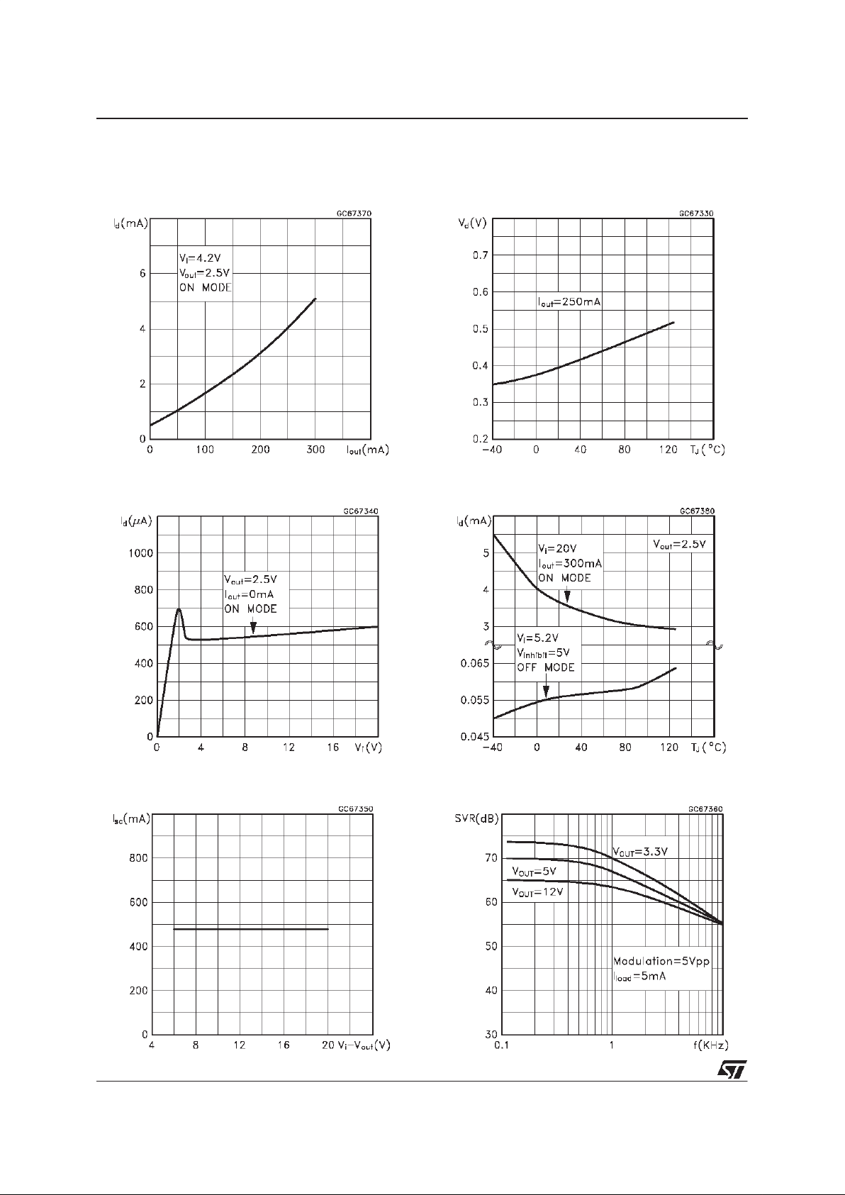
SupplyCurrent vs Output Current
SupplyCurrent vs Input Voltage
Short Circuit Currentvs Dropout Voltage
SupplyCurrent vs Temperature
S.V.R.vs InputVoltage Signal Frequency
TYPICALPERFORMANCE CHARACTERISTICS
(unlessotherwisespecified T
j
=25oC)
Dropout Voltagevs Temperature
L4931 SERIES
20/25

DIM.
mm inch
MIN. TYP. MAX. MIN. TYP. MAX.
A 4.8 0.189
C 1.37 0.054
D 2.4 2.8 0.094 0.110
D1 1.2 1.35 0.047 0.053
E 0.35 0.55 0.014 0.022
F 0.61 0.94 0.024 0.037
F2 1.15 1.4 0.045 0.055
G 4.95 5.08 5.21 0.195 0.200 0.205
H2 10.4 0.409
H3 10.05 10.4 0.396 0.409
L2 16.2 0.638
L3 26.3 26.7 27.1 1.035 1.051 1.067
L5 2.6 3 0.102 0.118
L6 15.1 15.8 0.594 0.622
L7 6 6.6 0.236 0.260
Dia. 3.65 3.85 0.144 0.152
P011D
TO-220 MECHANICAL DATA
L4931 SERIES
21/25

DIM.
mm inch
MIN. TYP. MAX. MIN. TYP. MAX.
A 1.75 0.068
a1 0.1 0.25 0.003 0.009
a2 1.65 0.064
a3 0.65 0.85 0.025 0.033
b 0.35 0.48 0.013 0.018
b1 0.19 0.25 0.007 0.010
C 0.25 0.5 0.010 0.019
c1 45 (typ.)
D 4.8 5.0 0.188 0.196
E 5.8 6.2 0.228 0.244
e 1.27 0.050
e3 3.81 0.150
F 3.8 4.0 0.14 0.157
L 0.4 1.27 0.015 0.050
M 0.6 0.023
S 8 (max.)
0016023
SO-8 MECHANICALDATA
L4931 SERIES
22/25

DIM.
mm inch
MIN. TYP. MAX. MIN. TYP. MAX.
A 2.2 2.4 0.086 0.094
A1 0.9 1.1 0.035 0.043
A2 0.03 0.23 0.001 0.009
B 0.4 0.6 0.015 0.023
B2 5.2 5.4 0.204 0.212
C 0.45 0.6 0.017 0.023
C2 0.48 0.6 0.019 0.023
D 6 6.2 0.236 0.244
E 6.4 6.6 0.252 0.260
G 4.9 5.25 0.193 0.206
G1 2.38 2.7 0.093 0.106
H 9.35 10.1 0.368 0.397
L2 0.8 1 0.031 0.039
L4 0.6 1 0.023 0.039
0078180/B
PPAK MECHANICAL DATA
L4931 SERIES
23/25

DIM.
mm inch
MIN. TYP. MAX. MIN. TYP. MAX.
A 2.2 2.4 0.086 0.094
A1 0.9 1.1 0.035 0.043
A2 0.03 0.23 0.001 0.009
B 0.64 0.9 0.025 0.035
B2 5.2 5.4 0.204 0.212
C 0.45 0.6 0.017 0.023
C2 0.48 0.6 0.019 0.023
D 6 6.2 0.236 0.244
E 6.4 6.6 0.252 0.260
G 4.4 4.6 0.173 0.181
H 9.35 10.1 0.368 0.397
L2 0.8 0.031
L4 0.6 1 0.023 0.039
==
D
L2
L4
13
==
B
E
==
B2
G
2
A
C2
C
H
A1
DETAIL”A”
A2
DETAIL”A”
TO-252 (DPAK) MECHANICAL DATA
0068772-B
L4931 SERIES
24/25

Information furnished is believed to be accurate and reliable. However, STMicroelectronics assumes no responsibility forthe consequences
of use of such information nor for any infringement of patents or other rights of third parties which may result from its use. No license is
granted by implication or otherwise under any patent or patent rights of STMicroelectronics. Specification mentioned in thispublication are
subject to change without notice. This publication supersedes and replaces all information previously supplied. STMicroelectronics products
are not authorized for use as critical components in life support devices or systems without express written approval of STMicroelectronics.
The ST logo is a trademarkof STMicroelectronics
1999 STMicroelectronics – Printed in Italy – All Rights Reserved
STMicroelectronics GROUP OF COMPANIES
Australia - Brazil - Canada - China -France -Germany - Italy - Japan - Korea -Malaysia - Malta - Mexico -Morocco - The Netherlands -
Singapore - Spain - Sweden - Switzerland - Taiwan - Thailand - UnitedKingdom - U.S.A.
http://www.st.com
.
L4931 SERIES
25/25
 Loading...