

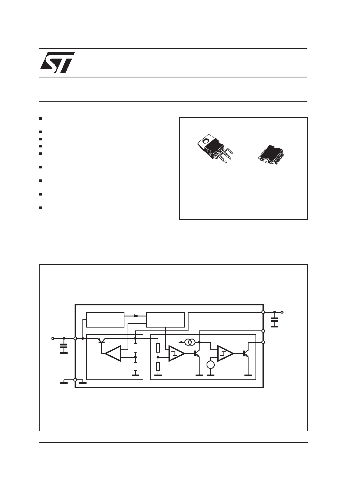
VERY LOW DROP VOLTAGE REGULATOR
OPERATINGDC SUPPLY VOLTAGERANGE
6V TO 28V
TRANSIENTSUPPLYVOLTAGEUP TO 40V
EXTREMELY LOW QUIESCENTCURRENT
HIGHPRECISIONOUTPUT VOLTAGE
OUTPUT CURRENT CAPABILITY UP TO
500mA
VERY LOW DROPOUT VOLTAGE LESS
THAN 0.6V
RESET CIRCUIT SENSING THE OUTPUT
VOLTAGE
PROGRAMMABLE RESET PULSE DELAY
WITH EXTERNALCAPACITOR
THERMAL SHUTDOWN AND SHORT CIR-
CUIT PROTECTIONS
Pentawatt
ORDERING NUMBERS:
L4925
PowerSO20
L4925 (Pentawatt)
L4925PD (PowerSO20)
DESCRIPTION
The L4925 is a monolithic integrated 5V voltage
regulator with a very low dropoutoutput and addi-
BLOCK DIAGRAM
PREREGULATOR
5V
V
S
C
S
GND
Vz
VREF
1.23V
+
-
tional functions such as power-on reset and programmable reset delay time. It is designed for
supplying microcomputer controlled systems especiallyin automotiveapplications.
L4925N
CT
Vz
2µ
2V
=
RESETREG
D95AT151
RES
V
O
June 2000
This is advanced informationon a newproduct now in development or undergoing evaluation.Details are subject to change withoutnotice.
1/8
L4925
ABSOLUTE MAXIMUM RATINGS
Symbol Parameter Value Unit
V
SDC
V
STR
I
O
V
O
V
RES
I
RES
T
stg
T
j
T
j-SD
NOTE:
The circuit is ESD protected according to MIL-STD-883C. According to ISO/DIS 7637 the transients must be clamped with external circuitry
(see Application Circuit).
CONNECTIONDIAGRAM
DC Operating Supply Voltage 28 V
Transient Supply Voltage (t < 1s) 40 V
Output Current internally limited
Output Voltage 20 V
Output Voltage 20 V
Output Current 5 mA
Storage Temperature -55 to 150
C
°
Operating Junction Temperature -40 to 150 °C
Thermal Shutdown-Junction Temperature 165 °C
N.C.
N.C.
V
S
V
S
N.C.
N.C.
RES
N.C.
N.C. N.C.
GND N.C.
2
3
4
5
6
7
8
9
10
D95AT152
20
19
18
17
16
15
14
13
12
11
THERMAL DATA
Symbol Parameter Pentawatt SO 20 Unit
R
th j-amb
R
th j-case
Thermal resistance junction to ambient max.
Thermal resistance junction to case max.
60
3.5
77 to 97 °C/W
N.C.1
N.C.
N.C.
VOUT
VOUT
N.C.
CT
N.C.
°C/W
2/8
L4925
ELECTRICALCHARACTERISTICS
=14VTj=–40 to 125°C unless otherwise specified;
(V
S
Symbol Parameter Test Condition Min. Typ. Max. Unit
V
O
V
O
V
DP
V
IO
Output Voltage VI= 6 to28V; IO= 1 to 500mA 4.90 5 5.10 V
Output Voltage VI= 35V; T <1s;
I
= 1 to 500mA
O
Dropout Voltage IO= 100mA
I
= 500mA
O
Input to Output Voltage
V
= 4V; IO= 100mA 0.5 V
I
0.2
0.3
5.50 V
0.3
0.6
Difference in Undervoltage
Condition
V
I
V
I
LIM
QSE
OL
OLO
I
Q
Line Regulation VI = 6 to 28V; IO= 1 to1mA 10 mV
Load Regulation IO= 1 to 500mA 50 mV
Current Limit VO= 4.5V
VO= 0;Foldback characteristic
;
550 1000
250
1500 mA
Quiescent Current IO= 0.3mA 190 360 µA
Quiescent Current IO= 500mA 20 mA
RESET
Symbol Parameter Test Condition Min. Typ. Max. Unit
V
V
t
t
V
I
V
V
CTth hy
RT
RTH
RD
RR
RL
RH
CTth
Reset Threshold Voltage 4.5 5.2 V
Reset Threshold 50 100 200 mV
Reset Pulse Delay CT= 100nF; tR> 100µs 60 100 140 ms
Reset Reaction Time CT= 100nF; 5 30
Reset Output LOW Voltage R
Reset Output HIGH Leakage
= 10KΩ to VO;VS=> 3V 0.4 V
RES
V
=5V 1 µA
RES
Current
Delay Comparator Threshold 2 V
Delay Comparator Threshold
200 mV
Hysteresis
V
V
mA
µ
s
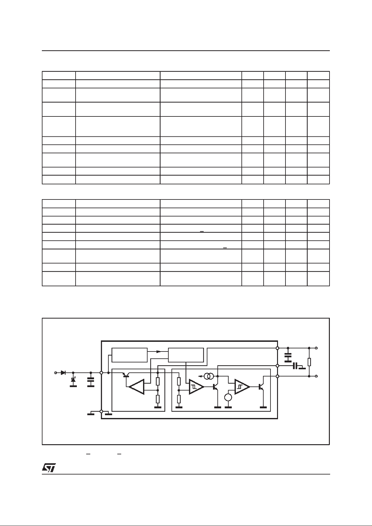
APPLICATIONCIRCUIT DIAGRAM
PREREGULATOR
5V
VBAT
For stability: C
Recommendedfor application:C
V
S
C
S
GND
>1µF; CO>10µF;ESR< 2.5Ωat 10KHz
S
S=CO
Vz
+
-
=10µF to100µF
VREF
1.23V
RESETREG
Vo
L4925N
Vz
2µ
2V
=
D95AT153
Co
CT
RES
Vout
RES
3/8

L4925
APPLICATIONNOTE
SUPPLYVOLTAGETRANSIENTS
High supply voltage transients can cause a reset
output signaldisturbation.
For supply voltage greater than 8V the circuit
shows a high immunityof the reset output against
supply transientsof morethan100V/µs.
For supply voltage lower than 8V, supply transients of more than 0.4V/µs. can cause a reset
signal disturbation.
FUNCTIONAL DESCRIPTION
The L4925 is a monolithic integrated voltage
regulator, based on the STM modular voltage
regulator approach. Several outstanding features
and auxiliary functions are implemented to meet
the requirements of supplying microprocessor
systems in automotiveapplications.
Nevetrheless, it is suitable also in other applications where the present functions are required.
The modular approachof thisdevice allows to get
easily also other features and functions when required.
VOLTAGEREGULATOR
The voltage regulator uses an Isolated Collector
Vertical PNP transistor as a regulating element.
With this structure very low dropout voltage at
currentsup to500mAis obtained.
FoldbackCharacteristicsOf Vo
The dropout operation of the standby regulator is
maintained down to 3V input supply voltage. The
output voltage is regulated up to the transient input supply voltage of 35V. With this feature no
functional interruption due to overvoltage pulses
is generated.
The typical curve showing the standby output
voltageas a functionof the input supply voltage is
shownin fig. 1.
The currentconsumption of the device (quiescent
current) is less than250µA.
To reduce the quiescent current peak in the undervoltage region and to improve the transient response in this region, the dropout voltage is controlled.
The quiescent current as a function of the supply
input voltage is shownin fig. 2.
Figure 1: OutputVoltagevs. Input Voltage
4/8
Figure2: QuiescentCurrent vs. SupplyVoltage

L4925
RESET CIRCUIT
The block circuit diagram of the reset circuit is
shown in Figure 3. The reset circuit supervises
the output voltage. The reset threshold of 4.5V is
defined with the internal reference voltage and
standby output divider.
The reset pulse delay time t
charge time of an external capacitor C
C
=
t
RD
, is defined with the
RD
x2V
T
2µA
:
T
Figure 3
The reaction time of the reset circuit originates
from the discharge time limitation of the reset capacitorC
and it is proportionalto the valueof CT.
T
The reaction time of thereset circuit increasesthe
noise immunity.Standby output voltage drops below the reset threshold only a bit longer than the
reaction time results in a shorter reset delay time.
The nominal reset delaytime will be generated for
standbyoutput voltage dropslonger thanapproximately 50µs. The typical reset output waveforms
are shown in Figure4.
Figure 4
5/8

L4925
DIM.
MIN. TYP. MAX. MIN. TYP. MAX.
mm inch
A 4.8 0.189
C 1.37 0.054
D 2.4 2.8 0.094 0.110
D1 1.2 1.35 0.047 0.053
E 0.35 0.55 0.014 0.022
E1 0.76 1.19 0.030 0.047
F 0.8 1.05 0.031 0.041
F1 1 1.4 0.039 0.055
G 3.2 3.4 3.6 0.126 0.134 0.142
G1 6.6 6.8 7 0.260 0.268 0.276
H2 10.4 0.409
H3 10.05 10.4 0.396 0.409
L 17.55 17.85 18.15 0.691 0.703 0.715
L1 15.55 15.75 15.95 0.612 0.620 0.628
L2 21.2 21.4 21.6 0.831 0.843 0.850
L3 22.3 22.5 22.7 0.878 0.886 0.894
L4 1.29 0.051
L5 2.6 3 0.102 0.118
L6 15.1 15.8 0.594 0.622
L7 6 6.6 0.236 0.260
L9 0.2 0.008
M 4.23 4.5 4.75 0.167 0.177 0.187
M1 3.75 4 4.25 0.148 0.157 0.167
V4 40°(typ.)
OUTLINE AND
MECHANICALDATA
Pentawatt V
A
H3
B
H1
L
L1
L8
VV
C
L5
Dia.
L7
L6
D1
V1
R
D
L2
L3
RESIN BETWEEN
V3
R
R
V4
F1
LEADS
H2
E
M1
M
V4
GG1
F
L9
VV
H2
F
E1
E
V4
6/8

L4925
DIM.
MIN. TYP. MAX. MIN. TYP. MAX.
mm inch
A 3.6 0.142
a1 0.1 0.3 0.004
a2 3.3
0.012
0.130
a3 0 0.1 0.000 0.004
b 0.4 0.53 0.016 0.021
c 0.23 0.32 0.009 0.013
D (1) 15.8 16 0.622 0.630
D1 9.4 9.8 0.370 0.386
E 13.9 14.5 0.547 0.570
e 1.27 0.050
e3 11.43 0.450
E1 (1) 10.9 11.1 0.429 0.437
E2 2.9
0.114
E3 5.8 6.2 0.228 0.244
G 0 0.1 0.000 0.004
H 15.5 15.9 0.610 0.626
h 1.1
0.043
L 0.8 1.1 0.031 0.043
N10°(max.)
S
8°(max.)
T 10 0.394
(1)”D andF” donot include moldflashor protrusions.
- Moldflash orprotrusions shallnot exceed 0.15mm (0.006”).
- Criticaldimensions: ”E”, ”G”and”a3”
OUTLINE AND
MECHANICAL DATA
JEDEC MO-166
PowerSO20
E2
hx
45
DETAIL B
BOTTOM VIEW
R
a3
Gage Plane
lead
E
DETAIL B
0.35
S
D1
a1
L
c
DETAIL A
slug
-C-
SEATING PLANE
GC
(COPLANARITY)
E3
NN
a2
A
b
DETAIL A
e3
H
D
T
1
e
1120
E1
10
PSO20MEC
7/8

L4925
Informat ionfurnishedis believed to be accurat e and reliable. However, STMicro electron icsassum e s no responsi bilit yfor the consequence s
of use of such informationnor forany infringement of patents or other rights of third parties which may result fromits use. No license is
grantedby implicationor otherwise under any patentor patentrightsof STMicroelectronics. Specificationmentioned in thispublicationare
subject to change withoutnotice. Thispublicationsupersedes andreplaces all informationpreviouslysupplied.STMicroelectronicsproducts
are notauthor izedforuse as cri tical componentsinlife supportdevicesor sys tems without expr es swrittenapprovalof STMicroelectronics.
The ST logois a registeredtrademarkof STMicroelectronics
2000STMicroelectronics – Printed in Italy – AllRightsReserved
STMicroelectronics GROUP OF COMPANIES
Australia - Brazil - China- Finland - France- Germany - Hong Kong - India - Italy - Japan - Malaysia - Malta - Morocco -
Singapore - Spain - Sweden- Switzerland - United Kingdom - U.S.A.
http://www.st.com
8/8
 Loading...