

L4920
VERY LOWDROP ADJUSTABLE REGULATORS
.
VERYLOWDROP VOLTAGE
.ADJUSTABLE OUTPUT VOLTAGE FROM
1.25VTO 20V
.400mAOUTPUTCURRENT
.LOWQUIESCENTCURRENT
.REVERSEVOLTAGEPROTECTION
.+ 60/ − 60VTRANSIENTPEAK VOLTAGE
PROTECTION
.SHORTCIRCUIT PROTECTION WITH FOLD-
BACKCHARACTERISTICS
.THERMAL SHUT-DOWN
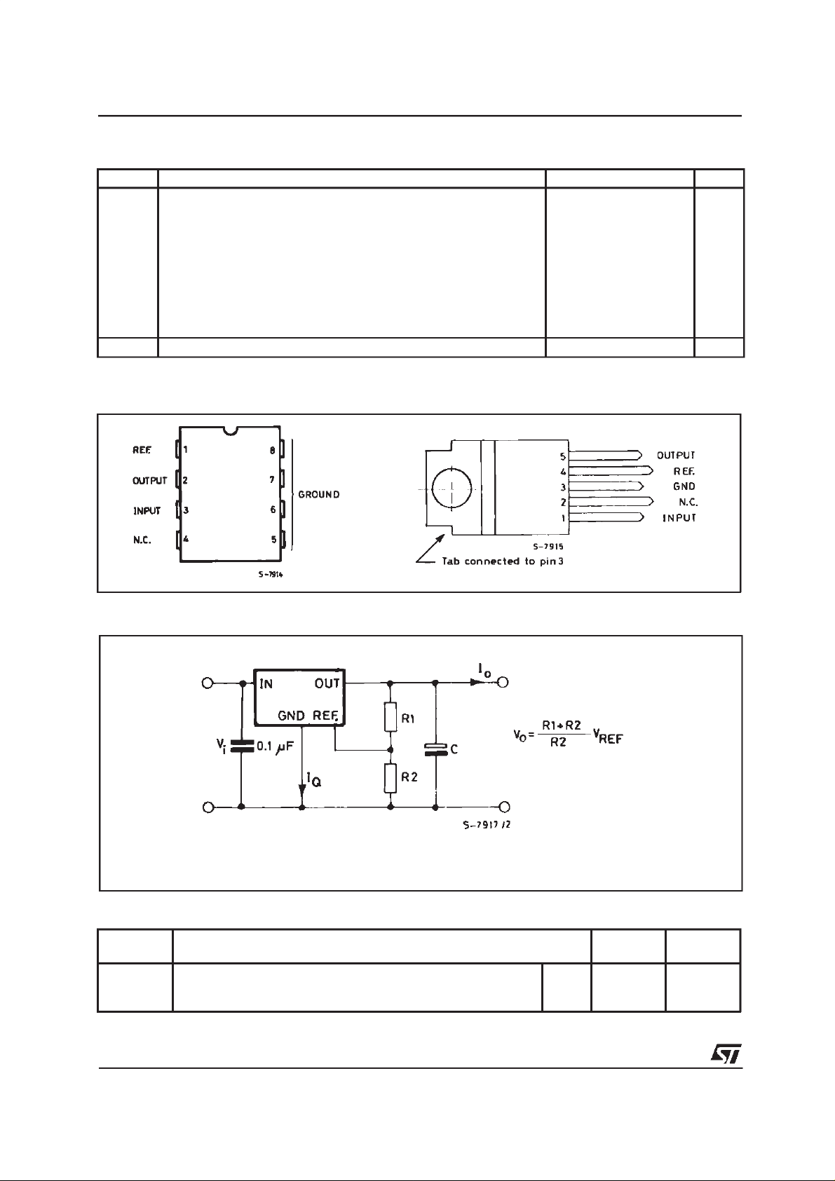
DES CRIPTION
The L4920and L4921 areadjustablevoltageregulatorswitha verylowvoltagedrop(0.4Vtyp.at 0.4A
=25°C), low quiescent current and comprehen-
T
j
siveon-chip protection.
Thesedevicesareprotectedagainstloaddumpand
field decay transients, polarity reversal and over
heating.
A foldbackcurrentlimiterprotectsagainstloadshort
circuits.
Theoutputvoltageisadjustablethroughanexternal
dividerfrom1.25V to 20V.The minimumoperating
input voltageis 5.2V (T
=25°C).
J
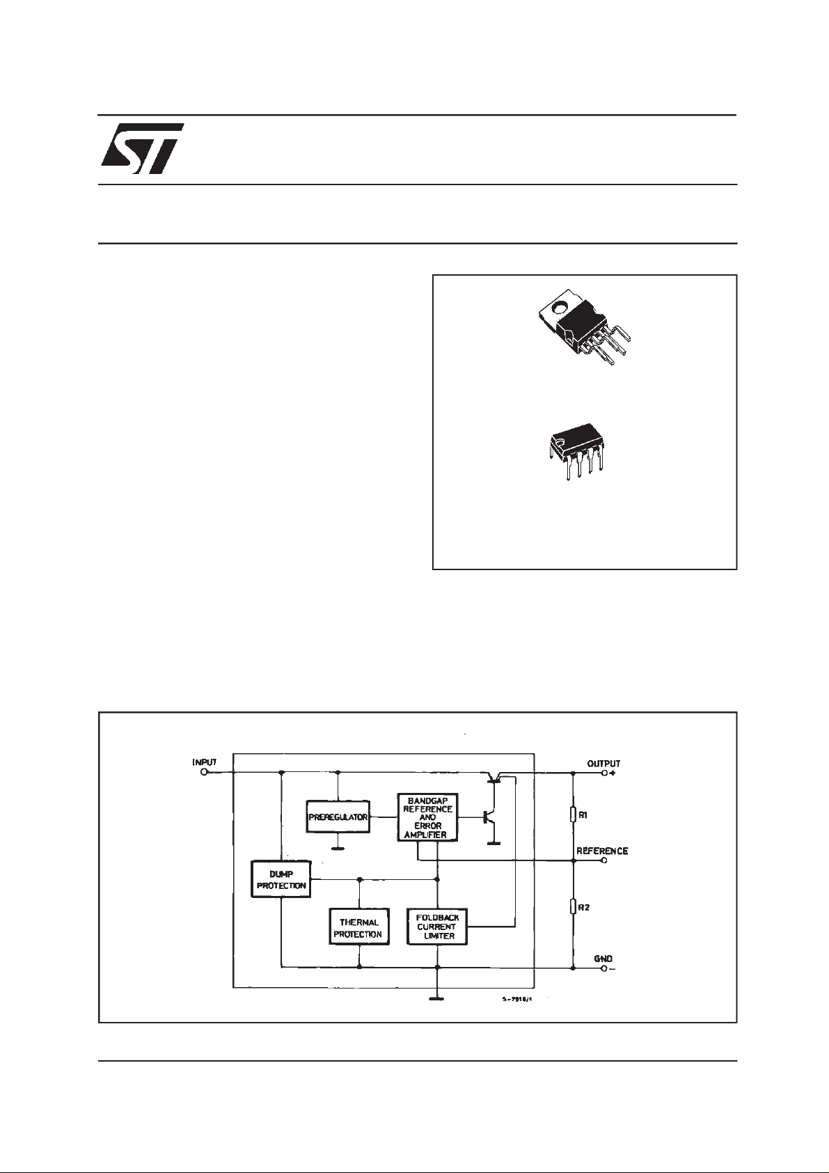
L4921
Pen tawatt
Minidip (4 + 4)
ORDERINGNUMBERS : L4920 (Pentawatt)
L4921(Minidip)
These regulators are designed for automotive, industrialand consumerapplicationswhere low consumptionisparticularlyimportant.
In batterybackupandstandbyapplicationsthelow
consumptionofthese devicesextendsbatterylife.
BLOCK DIAGRAM
June 2000
1/7
L4920/L4921
ABSOLUTE MAXIMUM RATINGS
Symbol Parameter Value Unit
DC Input Operating Voltage
V
i
DC Reverse Input Voltage
Transient Input Overvoltages:
Load Dump:
rise
10ms
≤
0.5
≥
Ω
5ms≤t
Fall timeconstant = 100ms
τ
f
R
SOURCE
Field Decay:
fall
10ms, R
≤
SOURCE
T
J,TSTG
5ms≤t
τ
Rise time constant = 33ms
f
Junction and Storage Temperature Range – 55 to 150
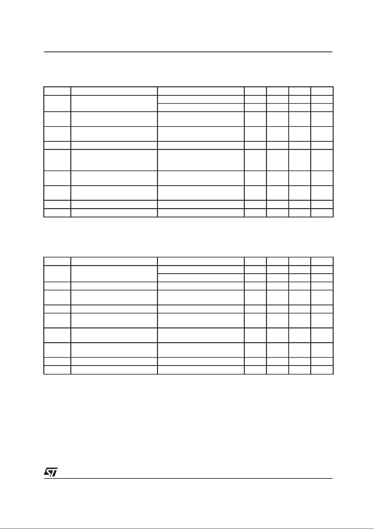
PIN CONNECTI ONS (top view)
≥10Ω
35 V
C
°
TEST AND APPLICATION CIRCUI T
C = 100µF is required for stability (ESR≤3Ωover T range)
R2 = 6.2KΩ.
THERMALDATA
Symbol Parameter Minidip
R
th j-amb
R
th j-pins
R
th j-case
Thermal Resistance Junction-ambient
Thermal Resistance Junction-pins
Thermal Resistance Junction-case
Max
Max
Max
80°C/W
15°C/W
(4 + 4)
–
Pentawatt
60°C/W
–
3.5 °C/W
2/7
L4920/L4921
ELECTRICALCHARACTERISTICS(forVI=14.4V,TJ=25°C,VO=5V,CO=100µF,unlessOtherwiseSpeci-
fied)
Symbol Parameter Test Condition Min. Typ. Max. Unit
Operating Input Voltage VO≥ 4.5V, IO= 400mA VO+0.7 26 V
V
I
V
< 4.5V, IO= 400mA 5.2 26 V
≤
O
1.20 1.25 1.30 V
≤ 400mA (*)
O
1 10 mV/V
400mA (*) V
≤
O
4.5V 3 15 mV/V
≥
O
0.05
0.2
0.4
0.4
0.7
V
V
V
V
∆V
∆
I
(* ) Foldbac k protection
Reference Voltage 5.2V < VI< 26V
REF
Line Regulation VO+1V<VI< 26V, VO≥ 4.5V
O
Load Regulation 5mA≤I
V
O
Dropout Voltage IO= 10mA
V
D
Quiescent Current IO= 0mA
I
Q
Maximal Output Current 800 mA
I
O
Short Circuit Output Current (*) 350 500 mA
OSC
V
REF
5mA ≤ I
= 5mA
I
O
= 150mA
I
O
= 400mA
I
O
+1V<VI<26V 0.8 2 mA
V
O
= 400mA (*)
I
O
V
+1V<VI<26V 65 90 mA
O
ELECTRICALCHARACTERISTICS (forVI=14.4V,–40≤ TJ≤ 125°C (note1),VO=5V,CO=100µF,unless
OtherwiseSpecified)
Symbol Parameter Test Condition Min. Typ. Max. Unit
Operating Input Voltage V
V
I
V
∆V
∆V
I
(*) Foldback protection.
Note : 1. Design limits are guaranteed (but not 100% production tested) over the indicated temperature and supply voltage
Reference Voltage 5.4V < VI< 26V 1.17 1.25 1.33 V
REF
Line Regulation VO+ 1.2V < VI< 26V, VO≥ 4.5V
O
Load Regulation 5mA ≤ IO≤ 400mA (*) VO≥ 4.5V 5 25 mV/V
O
Dropout Voltage IO= 150mA
V
D
Quiescent Current IO= 0mA
I
Q
Maximal Output Current 870 mA
I
O
Short Circuit Output Current (*) 230 500 mA
OSC
ranges. These limits are not used to calculate outgoing quality levels.
4.5V, I
≥
O
≤ VO< 4.5V, IO= 400mA 5.2 26 V
V
REF
= 400mA VO+0.9 26 V
O
2 15 mV/V
= 5mA
I
O
0.2
= 400mA
I
O
+ 1.2V < VI<26V 1,2 3 mA
V
O
= 400mA (*)
I
O
+ 1.2V < VI<26V 80 140 mA
V
O
0.4
0.4
0.7
V
V
3/7

L4920/L4921
Figure 1 :
Figure 3 :
OutputVoltagevs. Temperature.
QuiescentCurrentvs. OutputCurrent
=5V).
(V
o
Figure2 :
FoldbackCurrentLimiting.
APPLI CATI ON INFORMATIO N
1) TheL4920and L4921haveV
the outputvoltagecan beset downto V
mustbe greaterthan5.2V(Tj=25°C).
V
i
≅ 1.25V.Then
REF
REF
but
2) Astheregulatorreferencevoltage sourceworks
inclosedloop,thereferencevoltagemaychange
in foldbackcondition.
3) Forapplicationswith highV
, the total power
l
dissipation ofthedevice withrespectto the ther-
4/7
malresistanceof thepackagemaybe limiting. The
total powerdissipationis :
P
tot=Vilq
+(Vi-Vo)l
o
A typicalcurve giving the quiescentcurrent lqas a
functionof the outputcurrentl
is shownin fig.3.
o

L4920/L4921
DIM.
MIN. TYP. MAX. MIN. TYP. MAX.
A 3.3 0.130
a1 0.7 0.028
B 1.39 1.65 0.055 0.065
B1 0.91 1.04 0.036 0.041
b 0.5 0.020
b1 0.38 0.5 0.015 0.020
D 9.8 0.386
E 8.8 0.346
e 2.54 0.100
e3 7.62 0.300
e4 7.62 0.300
F 7.1 0.280
I 4.8 0.189
L 3.3 0.130
Z 0.44 1.6 0.017 0.063
mm inch
OUTLINE AND
MECHANICAL DATA
PowerMinidip
5/7

L4920/L4921
DIM.
MIN. TYP. MAX. MIN. TYP. MAX.
mm inch
A 4.8 0.189
C 1.37
0.054
D 2.4 2.8 0.094 0.110
D1 1.2 1.35 0.047 0.053
E 0.35 0.55 0.014 0.022
E1 0.76 1.19 0.030 0.047
F 0.8 1.05 0.031 0.041
F1 1 1.4 0.039 0.055
G 3.2 3.4 3.6 0.126 0.134 0.142
G1 6.6 6.8 7 0.260 0.268 0.276
H2 10.4 0.409
H3 10.05 10.4 0.396 0.409
L 17.55 17.85 18.15 0.691 0.703 0.715
L1 15.55 15.75 15.95 0.612 0.620 0.628
L2 21.2 21.4 21.6 0.831 0.843 0.850
L3 22.3 22.5 22.7 0.878 0.886 0.894
L4 1.29 0.051
L5 2.6 3 0.102 0.118
L6 15.1 15.8 0.594
0.622
L7 6 6.6 0.236 0.260
L9 0.2 0.008
M 4.23 4.5 4.75 0.167 0.177 0.187
M1 3.75 4 4.25 0.148 0.157 0.167
V4 40°(typ.)
OUTLINE AND
MECHANICAL DATA
Pentawatt V
A
H3
B
H1
L
L1
L8
VV
C
L5
Dia.
L7
L6
D1
V1
R
D
L2
L3
RESIN BETWEEN
V3
R
R
V4
F1
LEADS
H2
E
M1
M
V4
GG1
F
L9
VV
H2
F
E1
E
V4
6/7

L4920/L4921
Information furnished is believed to be accurate and reliable. However, STMicroelectronics assumes no responsibility for the consequences of use of such information nor for any infringement of patents or other rights of third parties which may result from its use. No
license is granted by implication or otherwise under any patent or patent rights of STMicroelectronics. Specification mentioned in this
publication are subject to change without notice. This publication supersedes and replaces all information previously supplied. STMicroelectronics products are not authorized for use as critical components in life support devices or systems without express written
approval of STMicroelectronics.
Australia - Brazil - China - Finland - France - Germany - Hong Kong - India - Italy - Japan - Malaysia - Malta - Morocco -
The ST logo is a registered trademark of STMicroelectronics
2000STMicroelectronics – Printed in Italy– All Rights Reserved
STMicroelectronics GROUP OF COMPANIES
Singapore - Spain - Sweden - Switzerland - United Kingdom- U.S.A.
http://www.st.com
7/7
 Loading...