


DUAL5V REGULATOR WITH RESET
.
OUTPUTCURRENTS : I01=50mA
I
=100mA
02
.
FIXEDPRECISIONOUTPUTVOLTAGE
±
5V
2%
.
RESETFUNCTION CONTROLLED BY INPUT
VOLTAGEAND OUTPUT 1 VOLTAGE
.
RESET FUNCTION EXTERNALLY PROGRAMMABLETIMING
.
RESETOUTPUT LEVELRELATEDTO
OUTPUT2
.
OUTPUT 2 INTERNALLY SWITCHED WITH
ACTIVEDISCHARGING
.
LOW LEAKAGE CURRENT, LESS THAN 1µA
ATOUTPUT 1
.
LOWQUIESCENTCURRENT (Input 1)
.
INPUT OVERVOLTAGE PROTECTION UP TO
60V
.
RESETOUTPUT NORMALLY HIGH
.
OUTPUTTRANSISTORSSOAPROTECTION
.
SHORT CIRCUIT AND THERMAL OVERLOADPROTECTION
Minidip
ORDERING NUMBER :
L4904A
L4904A
DESCRIPTION
The L4904A is a monolithic low drop dual 5V
regulatordesignedmainlyforsupplyingmicroprocessorsystems.
Resetand data savefunctionsduring switchon/off
canbe realized.
PIN CONNECTION
June 2000
1/9
L4904A
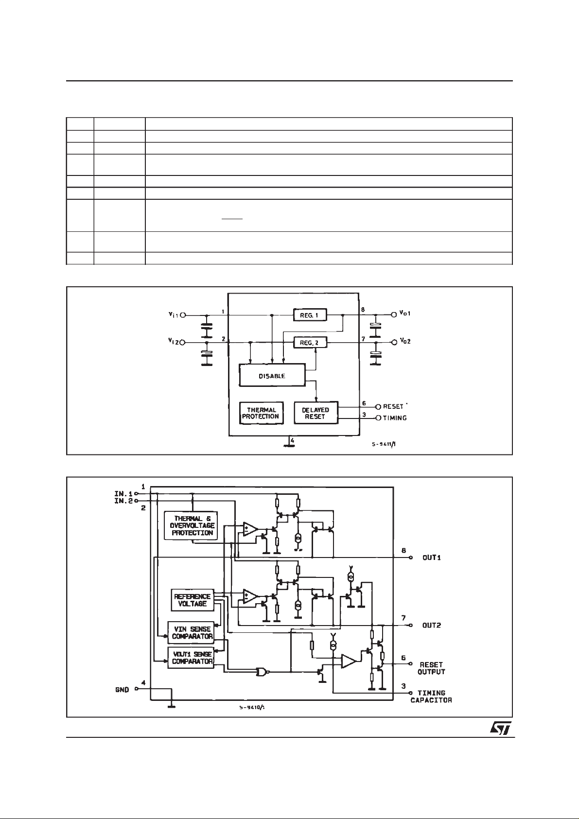
PIN FUNCTIONS
N°
1 Input 1 Low Quiescent Current 50mA Regulator Input.
2 Input 2 100mA Regulator Input.
3 Timing
4 GND Common Ground.
5 N.C. Not connected.
6 Reset
7 Output 2 5V – 100mA Regulator Output. Enabled if V
8 Output 1 5V – 50mA regulator output with low leakage in switch-OFF condition.
BLOCKDIAGRAM
Name Function
If Reg. 2 is switching-ON the delay capacitor is charged with a 10µA constant current. When
Capacitor
Reg. 2 is switched-OFF the delay capacitor is discharged.
When pin 3reaches 5V the reset output is switchedhigh.
Output
Therefore t
the C
capacitor is discharged.
o2
RD=Ct
5V
(
); tRD(ms) = Ct(nF).
10µA
1>VRTand V
o
IN 2>VIT
. If Reg. 2 is switched-OFF
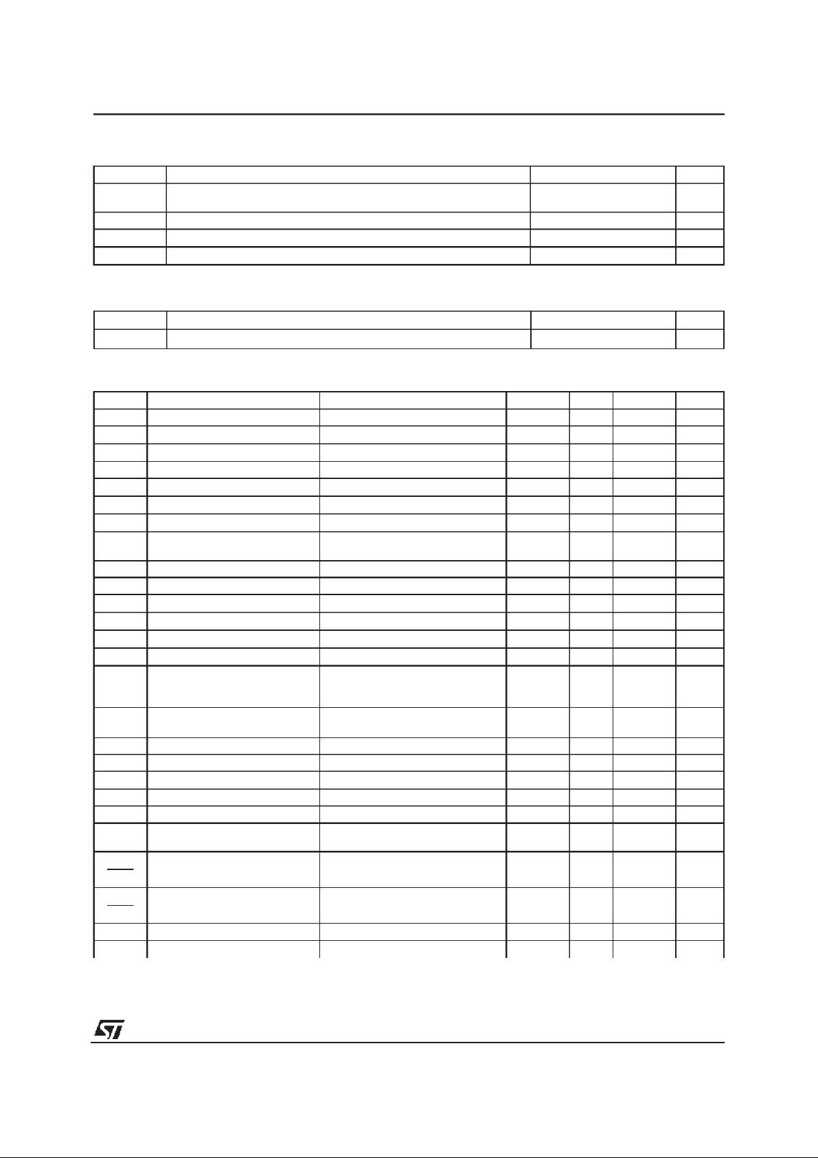
SCHEMATIC DIAGRAM
2/9
ABSOLUTEMAXIMUM RATINGS
Symbol Parameter Value Unit
V
IN
I
o
P
tot
T
DC Input Voltage
Transient Input Overvoltage (t = 40ms)
Output Current Internally Limited
Power Dissipation at T
Storage and Junction Temperature – 40 to 150
j
amb
=50°C
24
60
1W
THERMALDATA
Symbol Parameter Value Unit
R
th j-amb
Thermal ResistanceJunction-ambient Max 100
L4904A
V
V
°C
°C/W
ELECTRICAL CHARACTERISTICS
(V
IN
= 14.4V,T
=25oC unlessotherwise specified)
amb
Symbol Parameter Test Conditions Min. Typ. Max. Unit
V
DC Operating Input Voltage 20 V
i
V
Output Voltage1
01
V
V
V
V
∆V
∆
∆
∆
Output Voltage2 HIGH
02 H
Output Voltage2 LOW I02= – 5mA 0.1 V
02 L
I
Output Current 1 ∆
01
I
Leakage Output 1 Current
L01
I
Output Current 2 ∆
02
Output 1 Dropout Voltage (*) I01= 10mA
I01
V
Input Threshold Voltage V01+ 1.2 6.4 V01+ 1.7 V
IT
Input Threshold Voltage Hyst. 250 mV
ITH
Line Regulation 7V < VIN< 18V, I01= 5mA 5 50 mV
01
Line Regulation 2 7V < VIN< 18V, I02= 5mA 5 50 mV
V
02
Load Regulation 1 VIN= 8V, 5mA < I01< 50mA 5 20 mV
V
01
Load Regulation 2 VIN= 8V, 5mA < I02< 100mA 10 50 mV
V
02
IQ Quiescent Current
Quiescent Current 1 6.3V < V
I
Q1
V
V
V
V
∆V
∆
S
S
* The dropout voltage is defined as the differencebetween the input and the output voltage when the output voltage is lowered of 25 mV under
constant output current condition.
Reset Threshold Voltage V02–0.15 4.9 V02– 0.05 V
RT
Reset Threshold Hysteresis 30 50 80 mV
RTH
Reset Output Voltage HIGH
RH
Reset Output Voltage LOW IR= – 5mA 0.25 0.4 V
RL
t
Reset Pulse Delay Ct= 10nF 3 11 ms
RD
t
Timing Capacitor Discharge
d
Time
01
Thermal Drift
T
∆
V
02
Thermal Drift – 20°C≤<0>T
∆T
Supply Voltage Rejection f = 100Hz, VR= 0.5V, Io= 50mA 50 84 dB
VR1
Supply Voltage Rejection f = 100Hz, VR= 0.5V, Io= 100mA 50 80 dB
VR2
R Load 1kΩ
R Load 1kΩ
= – 100mV
V
01
=0,V01≤ 3V
V
IN
= – 100mV
V
02
= 50mA
I
01
I
02=I01
0<V
7V < V
I
01
I
R
5mA
≤
< 13V
IN
< 13V
IN
< 13V, V
IN1
≤ 5mA, I02=0
= 500µA
IN2
=0
Ct= 10nF 20
–20°C≤<0>T
amb
amb
≤ 125°C
125°C
≤
4.95 5.05 5.15 V
V01–0.1 5 V
01
50 mA
1
100 mA
0.7
0.75
4.5
1.6
0.8
0.9
6.5
3.5
0.6 0.9 mA
V
– 1 4.12 V
02
02
0.3
–0.8
0.3
– 0.8
V
µA
V
V
mA
V
µs
mV/°C
mV/°C
3/9

L4904A
TESTCIRCUIT
Figure1 : P.C.Board and ComponentsLayoutof the Test Circuit (1:1 scale)
APPLICATIONINFORMATION
Inpower suppliesfor µPsystems it is necessaryto
provide power continuously to avoid loss of informationin memoriesand in time of dayclocks,or to
savedatawhen theprimarysupplyisremoved.The
L4904A makes it very easy to supply such equipments;itprovidestwo voltageregulators(booth5V
high precision) with separate inputs plus a reset
output forthe data savefunction.
CIRCUITOPERATION(see Figure 2)
After switch on Reg. 1 saturatesuntil V
rises to
01
the nominalvalue.
When the input 2 reaches V
higherthanV
the reset output (V
grammabletime T
V
andVRareswitchedtogetherat lowlevelwhen
02
theoutput 2 (V02) switcheson and
RT
) also goes high after a pro-
R
(timingcapacitor).
RD
and the output 1 is
IT
one of the followingconditionsoccurs :
- an input overvoltage
- an overloadon the output 1 (V
- a switchoff (V
IN<VIT-VITH
);
01<VRT
);
and they start againas before when the condition
is removed.
An overload on output 2 does not switchReg. 2,
and does not influenceReg.1.
TheV
outputfeatures:
01
- 5 V internal reference without voltage divider
between the output and the error comparator;
- very low drop series regulator element utilizing
mirrors ;
permit high output impedance and then very low
leakagecurrent even in powerdown conditions.
Thisoutputmaythereforebeusedtosupplycircuits
continuously, such as volatile RAMs, allowing the
use of a back-up battery. The V
regulator also
01
featureslowconsumption(0.6 mAtyp.)to minimize
batterydrainin applicationswhere theV
regulator
1
is permanentlyconnectedto a battery supply.
TheV
outputcan supply other non essential5 V
02
circuits which may be powered down when the
systemis inactive,or that must be powered down
to prevent uncorrect operation for supply voltages
belowthe minimumvalue.
Theresetoutputcanbe usedas a”POWERDOWN
INTERRUPT”, permitting RAM access only in correctpowerconditions,oras a”BACK-UPENABLE”
to transfer data into in a NV SHADOW MEMORY
when the supply is interrupted.
4/9

Figure2
L4904A
APPLICATIONSUGGESTIONS
Figure 3 shows an application circuit for a µP
system.
Reg.1 is permanently connected to a battery and
supplies a CMOS time-of-day clock and a CMOS
microcomputerchip with volatilememory.
Reg.2 maybe switched OFF when the system is
inactive.
Figure4 shows the L4904Awith a backup battery
onthe V
outputto maintaina CMOStime-of-day
01
Figure3
clock and a stand by type C-MOSµP. The reset
output makes surethat the RAM is forced into the
low consumption stand by state, so the access to
memory is inhibit and the back up battery voltage
cannotdrop so low that memory contents arecorrupted.
Inthis casethe mainon-offswitchdisconnectsboth
regulatorsfrom the supply battery.
Application Circuits of a Microprocessor system
(Figure3) or with data savebattery (Figure4). The
reset output provide delayed rising front at the
5/9

L4904A
Figure4
6/9

L4904A
Figure5 : QuiescentCurrent (reg. 1) versus
Output Current
Figure7 : TotalQuiescentCurrent versus
Input Voltage
Figure6 : QuiescentCurrent (reg. 1 versus
Input Voltage
Figure8 : SupplyVoltage Rejection
Regulators1 and 2 versus Input
Ripple Frequence
7/9

L4904A
DIM.
MIN. TYP. MAX. MIN. TYP. MAX.
A 3.32 0.131
a1 0.51 0.020
B 1.15 1.65 0.045 0.065
b 0.356 0.55 0.014 0.022
b1 0.204 0.304 0.008 0.012
D 10.92 0.430
E 7.95 9.75 0.313 0.384
e 2.54 0.100
e3 7.62 0.300
e4 7.62 0.300
F 6.6 0.260
I 5.08 0.200
L 3.18 3.81 0.125 0.150
Z 1.52 0.060
mm inch
OUTLINE AND
MECHANICAL DATA
Minidip
8/9

L4904A
Information furnished is believed to be accurate and reliable. However, STMicroelectronics assumes no responsibility for the
consequences of use of such information nor for any infringementof patents or other rights of third parties which may result from
its use. No license is granted by implication or otherwise under any patent or patent rights of STMicroelectronics. Specification
mentioned in this publication are subject to change without notice. This publication supersedes and replaces all information
previouslysupplied.STMicroelectronicsproducts arenot authorizedforuse ascriticalcomp onentsinlife support devicesorsystems
without express written approval of STMicroelectronics.
Australia - Brazil - China - Finland - France - Germany - Hong Kong - India - Italy - Japan - Malaysia - Malta - Morocco -
The ST logo is a registeredtrademark of STMicroelectronics
2000 STMicroelectronics – Printed in Italy – All Rights Reserved
STMicroelectronics GROUP OF COMPANIES
Singapore- Spain - Sweden - Switzerland - United Kingdom - U.S.A.
http://www.st.com
9/9
 Loading...