

WITH RESET AND DISABLE FUNCTIONS
.
OUTPUTCURRENTS : I01= 50mA
I
=100mA
02
.
FIXEDPRECISION OUTPUT VOLTAGE
5V ± 2%
.
RESETFUNCTION CONTROLLED BY INPUT
VOLTAGEANDOUTPUT1VOLTAGE
.
RESET FUNCTION EXTERNALLY PROGRAMMABLETIMING
.
RESET OUTPUT LEVEL RELATED TO OUTPUT2
.
OUTPUT 2 INTERNALLY SWITCHED WITH
ACTIVEDISCHARGING
.
OUTPUT2DISABLELOGICALINPUT
.
LOW LEAKAGECURRENT, LESS THAN 1µA
ATOUTPUT1
.
INPUTOVERVOLTAGEPROTECTIONUP TO
60V
.
RESETOUTPUT NORMALLYLOW
.
OUTPUTTRANSISTORS SOAPROTECTION
.
SHORT CIRCUIT AND THERMAL OVERLOADPROTECTION
L4903
DUAL 5V REGULATOR
PRELIMINARY DATA
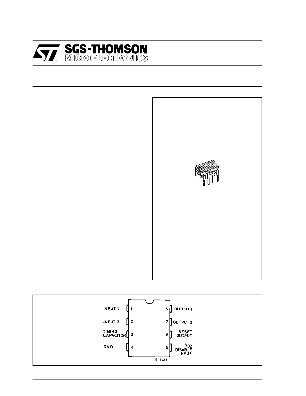
Minidip
ORDERING NUMBERS : L4903
DESCRIPTION
TheL4903 is a monolithic low dropdual 5 V regulatordesignedmainlyforsupplyingmicroprocessor
systems.
Reset, data save functions and remote switch
on/off controlcan be realized.
PIN CONNECTION
July1993
1/8
L4903
PIN FUNCTIONS
N° Name Function
1 Input1 Low Quiescent Current 50mA Regulator Input
2 Input2 100mA Regulator Input.
3 Timing
Capacitor
4 GND Common Ground
5 Disable Input A high level (> V
6 Reset Output When pin 3 reaches 5V the reset output is switched low.
7 Output 2 5V – 100mARegulator Output. Enabled if V
8 Output 1 5V– 50mA regulator output with low leakage inswitch-OFF condition.
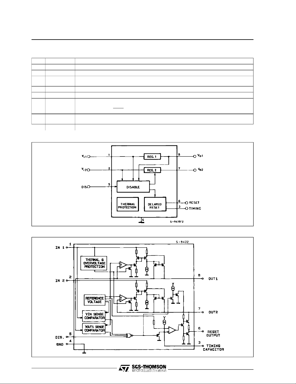
BLOCKDIAGRAM
If Reg. 2 is switched-ON the delay capacitor is charged with a 10µA constant current. When
Reg. 2 is switched-OFF the delaycapacitor isdischarged.
) disables output Reg. 2.
DT
5V
(
Therefore t
RD=Ct
If Reg. 2 is switched-OFF the C
);tRD(ms) = Ct(nF).
10µA
02
1>VRT. DISABLE INPUT < VDTand V
capacitor is discharged.
o
IN 2>VIT
.
SCHEMATIC DIAGRAM
2/8
ABSOLUTE MAXIMUMRATINGS
Symbol Parameter Value Unit
V
IN
V
P
tot
T
stg,Tj
DC Input Voltage 24 V
Transient Input Overvoltage (t =40ms) 60 V
t
Power Dissipation at T
=50°C1W
amb
Storage and Junction Temperature – 40 to 150 °C
THERMALDATA
Symbol Parameter Value Unit
R
th (j-pin)
R
th (j-a)
Thermal Resistance Junction-pin 4 Max. 70 °C/W
Thermal Resistance Junction-ambient Max. 100 °C/W
L4903
ELECTRICALCHARACTERISTICS (VIN= 14.4V,T
=25oC unless otherwise specified)
amb
Symbol Parameter Test Conditions Min. Typ. Max. Unit
V
V
V
02 H
V
02 L
I
01
I
L01
I
02
V
I01
V
V
ITH
∆V
∆V
∆V
∆V
IQ Quiescent Current I
I
Q1
V
RT
V
RTH
V
RH
V
RL
t
RD
t
V
DT
I
D
∆V
01
,
∆T
SVR1 Supply Voltage Rejection f = 100Hz, V
SVR2 Supply Voltage Rejection f = 100Hz, V
T
JSD
*The dropoutvoltage is defined as the difference between the input andthe output voltage when the output voltage is lowered of 25 mV under
constant output current condition.
DC Operating Input Voltage 20 V
i
Output Voltage 1 R Load 1kΩ 4.95 5.05 5.15 V
01
Output Voltage 2 HIGH R Load 1kΩ V01–0.1 5 V
Output Voltage 2 LOW I02= – 5mA 0.1 V
Output Current 1 max.(*) ∆V01= – 100mV 50 mA
Leakage Output 1 Current VIN=0,V01≤ 3V 1 µA
Output Current 2 max.(*) ∆V02= – 100mV 100 mA
Output 1 Dropout Voltage (*) I01= 10mA
= 50mA
I
01
Input Threshold Voltage V01+ 1.2 6.4 V01+ 1.7 V
IT
0.7
0.75
Input Threshold Voltage Hyst. 250 mV
Line Regulation 1 7V < VIN< 18V, I01= 5mA 5 50 mV
01
Line Regulation 2 7V < VIN< 18V, I02= 5mA 5 50 mV
02
Load Regulation 1 V
01
Load Regulation 2 V
02
Quiescent Current 1 6.3V < V
= 8V, 5mA < I01< 50mA 5 20 mV
IN1
= 8V, 5mA < I02< 100mA 10 50 mV
IN1
≤ 5mA
01=I02
< 13V
0<V
IN
7V < V
7V < V
I
01
< 13V V02LOW
IN
< 13V V02HIGH
IN
IN1
≤5mA, I02=0
< 13V, V
IN2
=0
4.5
2.7
1.6
0.6 0.9 mA
Reset Threshold Voltage V02– 0.04 4.7 V02– 0.02 V
Reset Threshold Hysteresis 30 50 80 mV
Reset Output Voltage HIGH IR= 500µAV
– 1 4.12 V
02
Reset Output Voltage LOW IR= – 5mA 0.25 0.4 V
Reset Pulse Delay Ct= 10nF 3 5 11 ms
Timing Capacitor Discharge
d
Time
Ct= 10nF 20 µs
V02DisableThreshold Voltage 1.25 2.4 V
V02DisableInput Current VD≤ 0.4V
∆V
02
Thermal Drift – 20°C ≤ T
∆T
≥ 2.4V
V
D
100mA
≤125°C
amb
= 0.5V, Io = 50mA 50 84 dB
R
= 0.5V, Io=
R
50 80 dB
-150
30
0.3
- 0.8
Thermal Shut Down 150 °C
0.8
0.9
6.5
4.5
3.5
01
V
V
V
mA
02
V
µA
µA
mV/°C
3/8

L4903
TESTCIRCUIT
Figure1 : P.C.Board and ComponentsLayout of theTestCircuit
APPLICATION INFORMATION
In power supplies forµP systemsit is necessaryto
provide power continuously to avoid loss of informationin memoriesand in time ofday clocks,or to
savedata whentheprimarysupplyisremoved.The
L4903 makes it very easy to supply such equipments; itprovidestwo voltageregulators(both 5V
high precision) with separate inputs plus a reset
outputforthedata savefunctionandReg.2 disable
input.
CIRCUITOPERATION (see Figure2)
After switch on Reg. 1 saturatesuntil V
01
rises to
the nominal value.
When the input 2 reachesV
higherthan V
theoutput2 (V02andVR) switches
RT
on and the reset output (V
programmabletime T
V
is switched at low level and VRat high level
02
RD
and the output 1 is
IT
) goes low after a
R
(timingcapacitor).
when one of thefollowingconditions occurs ;
- a high level(> V
) is applied onpin 5 ;
DT
- an input overvoltage ;
- an overload on theoutput 1 (V
- a switch off(V
IN<VIT-VITH
);
01<VRT
);
and they start again as before when the condition
4/8
is removed.
An overload on output 2 does not switch Reg. 2,
and does not influenceReg. 1.
The V
output features:
01
- 5 V internal reference without voltage divider
between the output and the error comparator
- very low drop series regulator element utilizing
current mirrors
permit high output impedance and then very low
leakagecurrent even in power conditions.
Thisoutputmaythereforebe usedtosupplycircuits
continuously,such as volatile RAMs, allowing the
use of a back-upbattery.
The V
cansupplyother non essential5 V circuits
02
which may be powereddown when the system is
inactive, or thatmust bepowered down to prevent
uncorrect operation for supply voltages below the
minimumvalue.
Theresetoutputcanbeusedasa”POWERDOWN
INTERRUPT”, permittingRAM access only in correctpowerconditions,or asa ”BACK-UPENABLE”
to transferdata into in a NV SHADOW MEMORY
when the supplyis interrupted.
The disablefunction can beused for remote on/off
controlof circuits connectedto theV
output.
02

Figure2
L4903
APPLICATION SUGGESTION
Figure 3 illustrateshow the L4903’sdisable input
maybe used in a CMOS µComputerapplication.
TheV
regulator(lowconsumption)supplyperma-
01
nently a CMOS time of day clock and a CMOS
computer chip with volatile memory. V
02
output,
Figure3
supplyingnon-essentialcircuits, isturned OFF under control of a µPunit.
Configurations of this type are used in products
where the OFF switch is part of a keyboard
scanned by a micro which operates continuously
even in theOFF state.
5/8

L4903
Figure4 : QuiescentCurrent (reg.1) versus
OutputCurrent
Figure6 : TotalQuiescentCurrent versus
Input Voltage
Figure 5 : Quiescent Current (reg.1 versus
Input Voltage
Figure 7 : SupplyVoltage Rejection
Regulators1 and2 versusInput
Ripple Frequence
6/8

MINIDIPPACKAGE MECHANICAL DATA
L4903
DIM.
MIN. TYP. MAX. MIN. TYP. MAX.
A 3.32 0.131
a1 0.51 0.020
B 1.15 1.65 0.045 0.065
b 0.356 0.55 0.014 0.022
b1 0.204 0.304 0.008 0.012
D 10.92 0.430
E 7.95 9.75 0.313 0.384
e 2.54 0.100
e3 7.62 0.300
e4 7.62 0.300
F 6.6 0.260
I 5.08 0.200
L 3.18 3.81 0.125 0.150
Z 1.52 0.060
mm inch
7/8

L4903
Information furnished is believed to be accurate and reliable. However, SGS-THOMSON Microelectronics assumes no responsibility for the
consequences of useof such information nor for any infringement of patentsor other rights of third parties which may result from its use. No
license is granted by implicationor otherwise underany patentor patent rights ofSGS-THOMSON Microelectronics. Specifications mentioned
in this publication are subject to change without notice. This publication supersedes and replaces all information previously supplied.
SGS-THOMSON Microelectronics products arenotauthorizedfor useas critical components inlife supportdevices or systems withoutexpress
written approval of SGS-THOMSON Microelectronics.
1994 SGS-THOMSON Microelectronics - All Rights Reserved
Australia- Brazil - France - Germany - Hong Kong - Italy - Japan - Korea - Malaysia - Malta - Morocco - The Netherlands - Singa-
pore - Spain - Sweden - Switzerland - Taiwan - Thaliand - United Kingdom -U.S.A.
SGS-THOMSON Microelectronics GROUP OF COMPANIES
8/8
 Loading...