

Datasheet L4892CX, L4812CX, L4808CX, L4808CV, L4805CX Datasheet (SGS Thomson Microelectronics)
...
VERY LOW DROP VOLTAGE REGULATORS
.INPUT/OUTPUT DROP TYP. 0.4V
.400mAOUTPUT CURRENT
.LOW QUIESCENT CURRENT
.REVERSEPOLARITYPROTECTION
.OVERVOLTAGEPROTECTION(± 60V)
.FOLDBACKCURRENT LIMITING
.THERMAL SHUTDOWN
DESCRIP TION
L4805-L4885-L4892
L4808-L4810-L4812
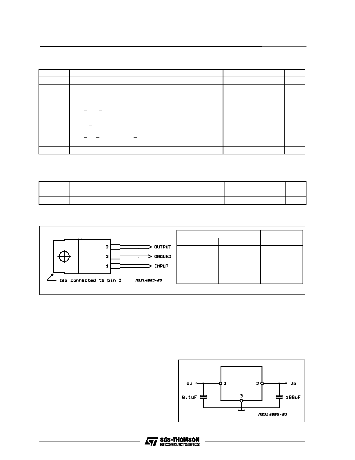
L4800series devicesare voltageregulatorswitha
verylowvoltagedrop(typically0.4Vatfullratedcurrent), output current up to 400mA, low quiescent
currentandcomprehensiveon-chipprotection.These devices are protected against load dump and
fielddecaytransientsof± 60V,polarityreversaland
overheating. A foldback current limiter protects
against load short circuits. Available in 5V, 8.5V,
9.2V,10Vand12Vversions(all±4%,T
seregulatorsaredesignedforautomotive,industrial
andconsumerapplicationswherelowconsumption
isparticularly important.
BLOCK DIAGRAM
=25°C)the-
I
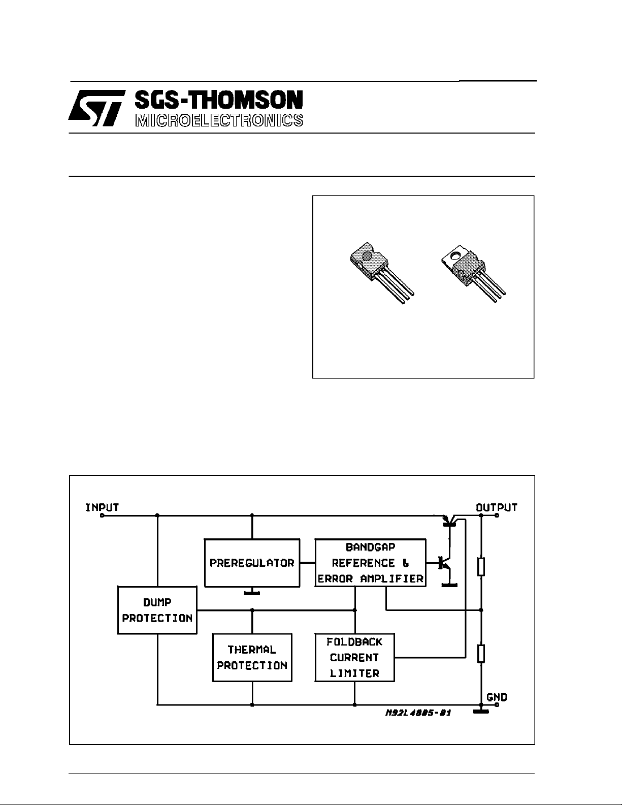
SOT-82
In automotiveapplicationstheL4805is ideal for 5V
logicsuppliesbecauseitcan operateevenwhenthe
batteryvoltagefallsbelow6V.Inbatterybackupand
standbyapplicationsthe low consumptionof these
devicesextendsbatterylife.
TO-220
March 1992
1/7
L4805-L4808-L4885-L4892-L4810-L4812
ABSOLUTE MAXIMUM RATINGS
Symbol Parameter Value Unit
V
I
T
j,Tstg
THERMAL DATA
Symbol Parameter SOT82 TO220 Unit
R
th j-case
R
th j-amb
DC Input Voltage + 35 V
DC Input Reverse Voltage - 18 V
Transient Input Overvoltages :
Load Dump :
5ms < T
τ
Fall Time Constant = 100ms,
f
R
source
Field Decay :
5ms < t
τ
Rise Time Constant = 33ms
r
Junction and Storage Temperature Range - 55 to + 150 °C
Thermal Resistance Junction-case Max. 8 4 °C/W
Thermal Resistance Junction-ambient Max. 100 75 °C/W
< 10ms,
rise
< 0.5Ω
< 10ms, R
fall
source
<10Ω
60
-60
V
V
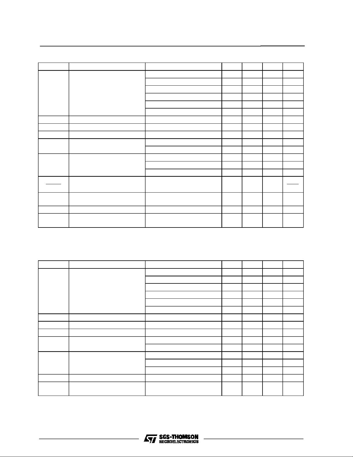
PIN CONNECTIO N (t o p view )
TEST AND APP LICAT ION CIRCUI T
Theoutputcapacitorisrequiredforstability. Though
the 100 µF shown is the minimum recommended
value, actual size and type may vary dep ending
upon the application load and temperaturerange.
Capacitoreffectiveseriesresistance(ESR)alsofactors in theIC stability.Since ESR varies from one
brand tothenext,somebenchworkmayberequired
todetermine the minimum capacitorvaluetousein
production.Worst-caseis usuallydeterminedatthe
minimumambienttemperature and maximumload
expected.
Outputcapacitorscan be increased in size to any
desired value above the minimum. One possible
purposeof this wouldbetomaintaintheoutput voltagesduringbrief conditions of negativeinputtransients that might be characteristics of a particular
system.
Order Codes
TO-220 SOT-82
L4805CV
L4808CV
L4885CV
L4892CV
L4810CV
L4812CV
L4805CX
L4808CX
L4885CX
L4892CX
L4810CX
L4812CX
OutputVoltage
5V
8V
8.5 V
9.2 V
10 V
12 V
Capacitors mustalsoberatedat allambienttemperatureexpected inthesystem.Manyaluminumtype
electrolyticswill freezeat temperatures less than –
30 °C, reducing their effectivecapacitanceto zero.
To maintainregulatorstabilitydown to –40 °C, capacitors rated at that temperature (such as tantalums)must be used.
2/7
L4805-L4808-L4885-L4892-L4810-L4812
ELECTRICAL CHARACTERISTICS (VI= 14.4V; CO= 100µF; Tj=25°C unlessotherwise specified.)
Symb o l Parame t er Test Con dition Min . Typ. Max. Uni t
V
V
∆V
∆V
V
I-VO
∆V
∆T•V
SVR
I
I
O
I
O/VO
O/VO
I
q
O
SC
Output Voltage IO= 5mA to 400mA (L4805) 4.80 5.00 5.20 V
= 5mA to 400mA (L4808) 7.68 8.00 8.32 V
I
O
= 5mA to 400mA (L4810) 8.16 8.50 8.84 V
I
O
= 5mA to 400mA (L4812) 8.83 9.20 9.57 V
I
O
= 5mA to 400mA (L4885) 9.60 10.00 10.40 V
I
O
= 300mA (L4892) 11.50 12.00 12.50 V
I
O
Operating Input Voltage 26 V
Line Regulation VI = 13 to 26V; IO= 5mA 1 10 mV/V
Load Regulation IO = 5 to 400mA* 3 15 mV/V
Dropout Voltage IO= 400mA* 0.4 0.7 V
= 150mA 0.2 0.4 V
I
O
Quiescent Current IO= 0mA 0.8 2 mA
= 150mA 25 45 mA
I
O
= 400mA* 65 90 mA
I
O
Temperature Output Voltage
O
Drift
O
Supply Voltage Rejection I
= 350mA; f = 320Hz;
O
=100µF; VI=VO+3V+2V
C
O
pp
0.1
60 dB
Max Output Current 800 mA
Output Short Circuit Current
350 500 mA
(fold back condition)
mV
°C•V
* onlyfor L4892 the current test conditions is IO= 300mA
ELECTRICAL CHARACTERISTICS (VI= 14.4V; CO= 100µF; Tj= -40 to 125°C (note 1) unless
otherwisespecified.)
Symb o l Parame t er Test Con dition Min . Typ. Max. Uni t
Output Voltage IO= 5mA to 400mA (L4805) 4.70 5.00 5.30 V
= 5mA to 400mA (L4808) 7.50 8.00 8.50 V
I
O
= 5mA to 400mA (L4810) 8.00 8.50 9.00 V
I
O
= 5mA to 400mA (L4812) 8.65 9.20 9.75 V
I
O
= 5mA to 400mA (L4885) 9.40 10.00 10.60 V
I
O
= 300mA (L4892) 11.30 12.00 12.70 V
I
O
Operating Input Voltage see note 2 26 V
Line Regulation VI = 14 to 26V; IO= 5mA 2 15 mV/V
Load Regulation IO = 5 to 400mA* 5 25 mV/V
Dropout Voltage IO= 400mA* 0.5 0.9 V
= 150mA 0.25 0.5 V
I
O
Quiescent Current IO= 0mA 1.2 3 mA
= 150mA 40 70 mA
I
O
= 400mA* 80 140 mA
I
O
Max Output Current 870 mA
Output Short Circuit Current
230 mA
(fold back condition)
∆V
∆V
V
I-VO
V
O
V
I
O/VO
O/VO
I
q
I
O
I
SC
Notes : 1. This limitsare guaranteed by design, correlation and statistical controlon production samples over the indicatedtemperature and
supply voltage ranges..
2. For a DCvoltage26V < Vi < 35V the deviceis not operating.
3/7

L4805-L4808-L4885-L4892-L4810-L4812
Figure 1: DropoutVoltage vs. Output Current Figure 2: Quiescent Current vs. OutputCurrent
Figure 3: Output Voltage vs. Temperature
Figure 4: FoldbackCurrent Limiting(L4805)
Figure 5: Preregulator for Distributed Supplies
4/7
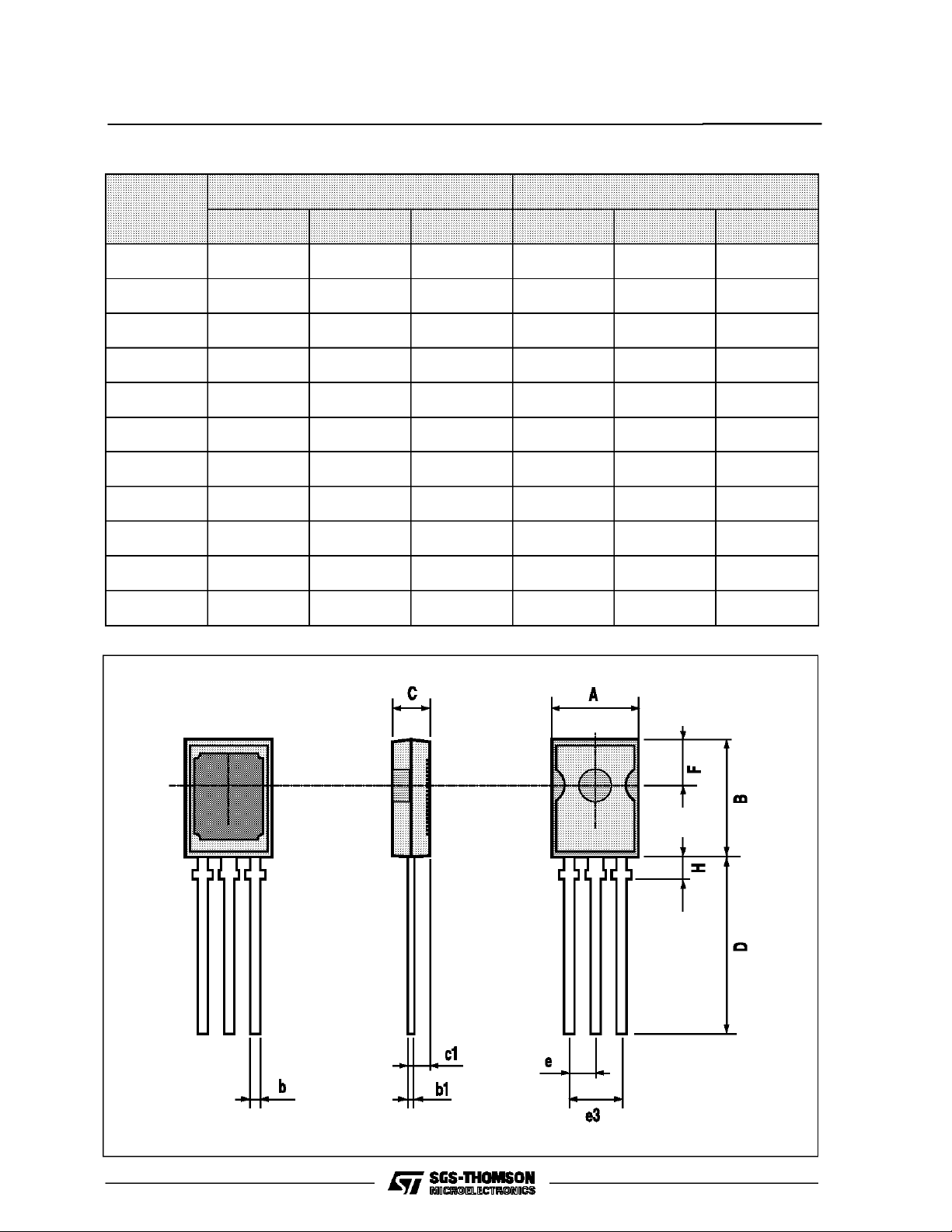
SOT82PACKAGE MECHANICAL DATA
L4805-L4808-L4885-L4892-L4810-L4812
DIM.
MIN. TYP. MAX. MIN. TYP. MAX.
A 7.4 7.8 0.291 0.307
B 10.5 10.8 0.413 0.425
b 0.7 0.9 0.028 0.035
b1 0.49 0.75 0.019 0.030
C 2.4 2.7 0.094 0.106
c1 1.2 0.047
D 15.7 0.618
e 2.2 0.087
e3 4.4 0.173
F 3.8 0.150
H 2.54 0.100
mm inch
5/7
L4805-L4808-L4885-L4892-L4810-L4812
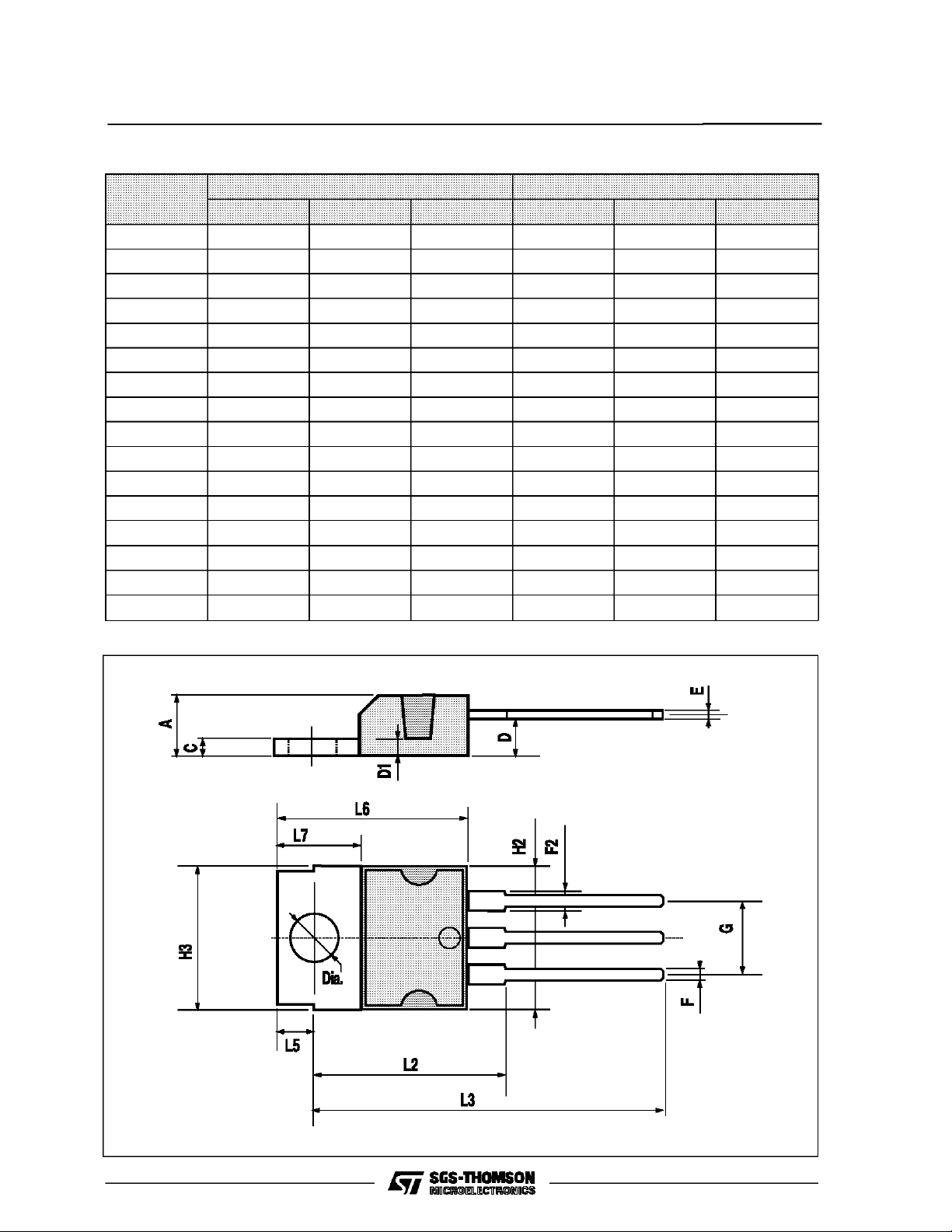
TO220PACKAGEMECHANICAL DATA
DIM.
MIN. TYP. MAX. MIN. TYP. MAX.
A 4.8 0.189
C 1.37 0.054
D 2.4 2.8 0.094 0.110
D1 1.2 1.35 0.047 0.053
E 0.35 0.55 0.014 0.022
F 0.8 1.05 0.031 0.041
F2 1.15 1.4 0.045 0.055
G 4.95 5.08 5.21 0.195 0.200 0.205
H2 10.4 0.409
H3 10.05 10.4 0.396 0.409
L2 16.2 0.638
L3 26.3 26.7 27.1 1.035 1.051 1.067
L5 2.6 3 0.102 0.118
L6 15.1 15.8 0.594 0.622
L7 6 6.6 0.236 0.260
Dia 3.65 3.85 0.144 0.152
mm inch
6/7

L4805-L4808-L4885-L4892-L4810-L4812
Information furnished is believed to be accurate and reliable. However, SGS-THOMSON Microelectronics assumes no responsibility for
the consequences of use of such information nor for any infringement of patents or other rights of third parties which may result from its
use. No license is granted by implication or otherwise under any patent or patent rights of SGS-THOMSON Microelectronics. Specifications mentioned in this publication are subject to change without notice. This publication supersedes and replaces all information previously supplied. SGS-THOMSON Microelectronics products are not authorized for use as critical components in life support devices or
systems without express written approval of SGS-THOMSON Microelectronics.
1994 SGS-THOMSON Microelectronics - All Rights Reserved
Australia - Brazil - France - Germany - Hong Kong - Italy - Japan - Korea - Malaysia - Malta- Morocco - The Netherlands - Singapore-
SGS-THOMSON Microelectronics GROUP OF COMPANIES
Spain - Sweden - Switzerland - Taiwan - Thaliand - United Kingdom - U.S.A.
7/7
 Loading...