

Page 1

L3100B
L3100B1
ApplicationSpecific Discretes
A.S.D.
FEATURES
UNIDIRECTIONALFUNCTION
PROGRAMMABLEBREAKDOWNVOLTAGE
UP TO265 V
PROGRAMMABLECURRENT LIMITATION
FROM50 mA TO550 mA
HIGHSURGECURRENTCAPABILITY
= 100A 10/1000µs
I
PP
DESCRIPTION
Dedicated to sensitive telecom equipment
protection, this device can provide both voltage
protection and current limitation with a very tight
tolerance.
Itshigh surgecurrentcapabilitymakes the L3100B
a reliable protection device for very exposed
equipment,or when seriesresistorsareverylow.
Thebreakdownvoltagecan beeasilyprogrammed
byusing an externalzenerdiode.
A multipleprotection mode canalso be performed
when using several zener diodes, providing each
lineinterface with an optimizedprotectionlevel.
The current limiting function is achieved with the
use of a resistor between the gate N and the
cathode. The value of the resistor will determine
thelevel of thedesired current.
OVERVOLTAGE AND OVERCURRENT
PROTECTION FOR TELECOM LINE
DIL 8
SCHEMATICDIAGRAM
Anode
Gate N Gate P
COMPLIESWITH THEFOLLOWING STANDARDS :
CCITTK17 - K20 10/700 µs 1.5 kV
5/310 µs38A
VDE0433 10/700 µs2 kV
5/200 µs50A
CNET 0.5/700 µs 1.5 kV
0.2/310 µs38A
TM: ASD is trademarks of SGS-THOMSON Microelectronics.
September 1998 Ed: 3A
Cathode
CONNECTION DIAGRAM
Gate N
NC
Gate P
Cathode
1
2
3
4
8
7
6
5
Anode
Anode
Anode
Anode
1/8
Page 2
L3100B/L3100B1
ABSOLUTE MAXIMUMRATINGS (T
Symbol Parameter Value Unit
amb
=25°C)
I
PP
I
TSM
Peakpulse current(see note 1) 10/1000µs
Nonrepetitivesurge peakon-state
current
T
stg
T
T
L
Note1 :
j
Storage temperaturerange
Maximumoperatingjunctiontemperature
Maximumleadtemperaturefor solderingduring 10s 230 °C
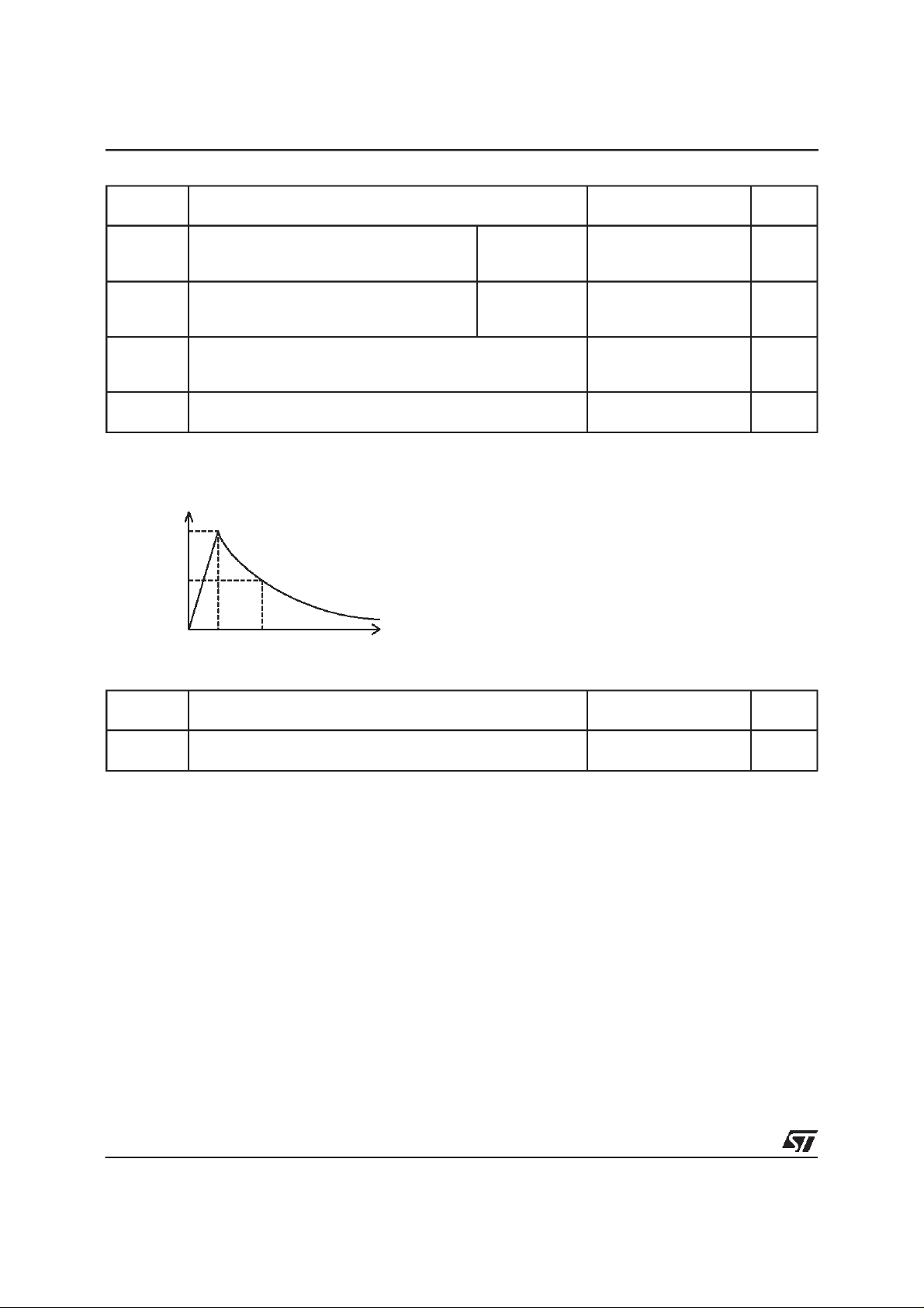
Pulsewaveform10/1000 µs
%I
PP
100
50
0
t
t
rp
THERMAL RESISTANCE
t
100
8/20 µs
250
tp= 10ms 50 A
- 40 to + 150
+ 150
°C
°C
A
Symbol Parameter Value Unit
2/8
R
th (j-a)
Junction-to-ambient 80 °C/W
Page 3
ELECTRICAL CHARACTERISTI CS(T
Symbol Parameter
amb
L3100B/L3100B1
=25°C)
V
RM
I
RM
V
BR
V
BO
I
H
I
BO
I
PP
V
GN
I
GN,IGP
V
RGN
C
Stand-offvoltage
Reverseleakagecurrent
Breakdownvoltage
Breakovervoltage
Holdingcurrent
Breakovercurrent
Peakpulse current
Gatevoltage
Triggeringgate current
Reversegate voltage
Capacitance
OPERATIONWITHOUT GATE
Type
max. min. max. min. max. min. max.
I
RM
@V
RM
I
I
I
I
VBR@I
pp
BO
H
RM
R
I
V
C
V
BO
V
RM
@I
BO
VBRV
I
BO
H
note1 note 1 note2
A V V mA V mA mA mA pF
µ
L3100B 6
40
L3100B1 6
40
60
250
60
250
265 1 350 200 500 280 100
255 1 350 200 500 210 100
OPERATIONWITH GATES
Type
V
GN@IGN
min. max. min. max. min. max.
= 200 mA IGN@VAC=100V V
@IG= 1mA IGP@VAC= 100V
RGN
V V mA mA V mA
L3100B/B1 0.6 1.8 30 200 0.7 150
Note 1 : See thereference test circuits for IH,IBOand VBOparameters.
Note 2 : VR= 5 V, F = 1MHz.
3/8
Page 4

L3100B/L3100B1
REFERENCE TESTCIRCUIT FOR IBOand VBOparameters:
=20ms
static
relay.
tp
K
I
BO
measure
Auto
Transformer
220V/2A
V
out
220V
Transformer
220V/800V
5A
TESTPROCEDURE:
PulseTest duration(tp = 20ms):
- For Bidirectionaldevices= Switch K is closed
- For Unidirectionaldevices= SwitchK is open.
Selection
V
OUT
- Devicewith V
-V
- Devicewith V
-V
BO
OUT
OUT
< 200 Volt
= 250V
≥ 200 Volt
BO
= 480V
RMS,R1
RMS,R2
=140Ω.
= 240 Ω.
R1
140
R2
240
D.U.T
V
BO
measure
FUNCTIONALHOLDING CURRENT(IH) TEST CIRCUIT= GO - NOGO TEST.
R
D.U.T .
V
= - 48 V
BAT
Surge generator
Thisis a GO-NOGOTestwhichallowsto confirmthe holdingcurrent (IH) levelina functionaltest
circuit.
Thistest canbe performedif thereference testcircuit can’tbe implemented.
TESTPROCEDURE:
1) Adjustthe currentlevel at theI
2) Firethe D.U.T with a surgeCurrent: Ipp= 10A , 10/1000 µs.
3) TheD.U.T will comebackto theOFF-Statewithina durationof 50 ms max.
valueby short circuitingthe AK of theD.U.T.
H
-V
P
4/8
Page 5

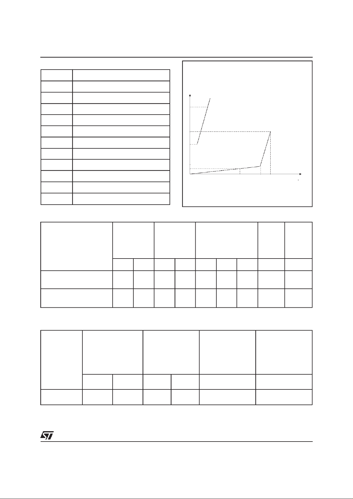
Figure 1
duration.
: Surge peak current versus overload
Figure 2
: Relative variation of holding current
versusjunctiontemperature.
L3100B/L3100B1
I (A)TSM
60
50
40
30
20
10
0
1E-2 1E-1 1E+0 1E+1 1E+2 1E+3
t(s)
F=50Hz
Tj initial=25°C
Figure3 :Relativevariation of breakdownvoltage
versusambienttemperature.
1.04
1.03
1.02
1.2
1.1
1.0
0.9
0.8
0.7
0 10203040506070
Figure 4 : Junction capacitance versus reverse
appliedvoltage.
100
80
60
1.01
1.00
0.99
0.98
0 10203040506070
40
20
0
110100
5/8
Page 6

L3100B/L3100B1
APPLICATION CIRCUIT
OvervoltageProtectionand Currentlimitation
PTC
+
A
L3100B\B1
C
G
N
HOOK
SPEECH
DIALING
RINGER
Ra
-
RINGER
Tablebelow gives the toleranceof thelimited currentITforeach standardizedresistorvalue.
Theformula(1) hasbeenused with V
valuesspecifiedat the typicalgate currentlevel IGN.
GN
CURRENTTOLERANCE
R
Ω
( ± 5%)
I
T
mA
min
I
T
mA
max
-
+
3.00
3.30
3.60
3.90
4.30
4.70
5.10
5.60
6.20
6.80
7.50
8.20
9.10
10.10
11.00
12.00
13.00
15.00
16.00
18.00
20.00
22.00
24.00
27.00
30.00
268
246
228
213
196
181
170
158
145
135
152
117
108
101
95
90
85
78
75
70
66
62
60
56
54
533
503
478
456
433
413
396
379
361
347
333
322
310
299
291
283
277
266
263
256
250
245
242
237
233
V
GN
L3100B
@I
GN
LOAD
Min. Max. Typ.
VVmA
0.75 0.95 100
6/8
Page 7

L3100B/L3100B1
Groundkey telephoneset Protection
PROTECTIONMODES:
ON HOOK =Ringer circuitprotection is ensuredwith breakdownvoltageat 265 V.
OFF HOOK = In dialingmode andin speech mode,the breakdownvoltage of L3100Bcan beadapted to
differentlevels withzener diodes.
ORDERCODE
L3100 B 1
VERSION.
=VBR =265 V
1 = VBR = 255 V
MARKING : Logo, DateCode,part Number.
7/8
Page 8

L3100B/L3100B1
PACKAGEMECHANICAL DATA.
DIL8 (Plastic)
I
a1
L
B
b
Z
e3
D
8
1
B1
e
5
4
DIMENSIONS
REF.
Millimetres Inches
Min. Typ. Max. Min. Typ. Max.
a1 0.70 0.027
b1
B 1.39 1.65 0.055 0.065
B1 0.91 1.04 0.036 0.041
F
b 0.5 0.020
b1 0.38 0.50 0.015 0.020
E
D 9.80 0.385
E 8.8 0.346
e 2.54 0.100
e3 7.62 0.300
F 7.1 0.280
I 4.8 0.189
L 3.3 0.130
Z 0.44 1.60 0.017 0.063
Weight:
0.59g
Packaging: Productsuppliedin antistatictubes.
Informationfurnished is believedtobe accurateand reliable. However,STMicroelectronicsassumes no responsIbilityfor theconsequences of
use ofsuch information nor for any infringementof patents or other rights of third parties which mayresult from its use.No license is granted by
implication or otherwise under any patent or patent rights of STMicroelectronics. Specifications mentioned in this publication are subject to
change withoutnotice. This publication supersedes and replaces all information previously supplied.
STMicroelectronics products are not authorized for use as critical components in life support devices or systems withoutexpress written approval ofSTMicroelectronics.
The ST logo is a registeredtrademark of STMicroelectronics
1998STMicroelectronics - Printed in Italy -All rights reserved.
STMicroelectronics GROUP OF COMPANIES
Australia -Brazil- Canada - China - France - Germany - Italy - Japan- Korea -Malaysia - Malta - Mexico- Morocco -
The Netherlands Singapore - Spain- Sweden - Switzerland -Taiwan - Thailand - UnitedKingdom - U.S.A.
8/8
 Loading...