


.OPERATINGSUPPLYVOLTAGEUP TO 46 V
.TOTALDC CURRENT UP TO 4 A
.
LOWSATURATIONVOLTAGE
.OVERTEMPERATUREPROTECTION
.
LOGICAL ”0” INPUT VOLTAGE UP TO 1.5 V
(HIGHNOISE IMMUNITY)
L298
DUALFULL-BRIDGE DRIVER
DESCRIPTION
TheL298isan integratedmonolithiccircuitin a 15lead Multiwatt and PowerSO20 packages. It is a
highvoltage,highcurrentdualfull-bridgedriver designedtoacceptstandardTTLlogiclevelsanddrive
inductiveloads such as relays, solenoids, DC and
steppingmotors.Twoenableinputsare providedto
enableordisablethedeviceindependentlyoftheinput signals.The emittersof thelowertransistorsof
each bridgeareconnectedtogetherand the correspondingexternalterminalcan beusedforthecon-
BLOCK DIAGRAM
Multiwatt15
ORDERING NUMBERS : L298N (M ultiwatt Vert.)
L298HN (Mult iwat t H oriz .)
L298P (PowerSO20)
nectionofanexternalsensingresistor.Anadditional
supplyinputis providedso that the logicworksat a
lowervoltage.
PowerSO20
Jenuary 2000
1/13
L298
ABSOLUTEMAXIMUM RATINGS
Symbol Parame t er Value Unit
V
V
V
I,Ven
V
P
T
T
stg,Tj
I
sens
Power Supply 50 V
S
LogicSupply Voltage 7 V
SS
Inputand Enable Voltage –0.3 to 7 V
Peak OutputCurrent (each Channel)
O
– Non Repetitive (t = 100µs)
–Repetitive (80% on –20% off; t
–DC Operation
= 10ms)
on
3
2.5
2
Sensing Voltage –1 to 2.3 V
tot TotalPower Dissipation (T
JunctionOperating Temperature –25 to 130 °
op
case
=75°C)
25 W
Storageand JunctionTemperature –40 to 150
A
A
A
C
°C
PIN CONNECTIONS
(top view)
Multiwatt15
TAB CONNECTED TO PIN 8
GND
Sense A
N.C.
Out 1
Out 2
V
S
Input 1
Enable A
Input 2
GND 10
1
2
3
4
PowerSO20
5
6
7
8
9
15
14
13
12
11
10
9
8
7
6
5
4
3
2
1
D95IN239
D95IN240A
20
19
18
17
16
15
14
13
12
11
CURRENT SENSING B
OUTPUT 4
OUTPUT 3
INPUT 4
ENABLE B
INPUT 3
LOGIC SUPPLY VOLTAGE V
GND
INPUT 2
ENABLE A
INPUT 1
SUPPLY VOLTAGE V
OUTPUT 2
OUTPUT 1
CURRENT SENSING A
GND
Sense B
N.C.
Out 4
Out 3
Input 4
Enable B
Input 3
VSS
GND
S
SS
THERMAL DATA
Symbol Parameter PowerSO20 Multiwatt15 Unit
R
th j-case
R
th j-amb
(*) Mountedon aluminumsubstrate
2/13
Thermal Resistance Junction-case Max. – 3
Thermal Resistance Junction-ambient Max. 13 (*) 35 °
°C/W
C/W

PIN FUNCTIONS(referto the block diagram)
MW .15 PowerSO Name Function
1;15 2;19 Sense A; Sense B Between this pin and ground is connected the sense resistorto
control thecurrent of the load.
2;3 4;5 Out 1; Out2 Outputs ofthe Bridge A; the currentthat flows throughthe load
connected between these two pins is monitored at pin 1.
46 V
S
Supply Voltage for the Power Output Stages.
A non-inductive 100nFcapacitor must be connected between this
pin and ground.
5;7 7;9 Input 1; Input 2 TTL CompatibleInputs of the BridgeA.
6;11 8;14 EnableA; Enable B TTL CompatibleEnable Input: theL statedisables the bridge A
(enable A) and/or the bridgeB (enable B).
8 1,10,11,20 GND Ground.
9 12 VSS Supply Voltage forthe Logic Blocks. A100nF capacitor must be
connected between this pin and ground.
10; 12 13;15 Input3; Input 4 TTL CompatibleInputs of the BridgeB.
13; 14 16;17 Out 3; Out 4 Outputs of the BridgeB. The current that flows throughthe load
connected between these two pins is monitored at pin 15.
– 3;18 N.C. NotConnected
ELECTRICALCHARACTERISTICS (VS= 42V; VSS=5V,Tj=25°C;unlessotherwise specified)
L298
Symb o l Parameter Test Co n d ition s Min. Typ. Max. Unit
Supply Voltage(pin 4) Operative Condition VIH+2.5 46 V
V
S
V
Logic SupplyVoltage (pin 9) 4.5 5 7 V
SS
Quiescent SupplyCurrent (pin 4) Ven=H; IL=0 Vi=L
I
S
=L Vi=X 4 mA
V
en
Quiescent Current from VSS(pin 9) Ven=H; IL=0 Vi=L
I
SS
=L Vi=X 6 mA
V
en
Input Low Voltage
V
iL
V
V
i
i
=H
=H
–0.3 1.5 V
13
50
24
7
22
70
36
12
mA
mA
mA
mA
(pins 5, 7, 10, 12)
V
Input High Voltage
iH
2.3 VSS V
(pins 5, 7, 10, 12)
I
Low Voltage Input Current
iL
Vi= L –10
A
µ
(pins 5, 7, 10, 12)
I
High Voltage Input Current
iH
Vi = H≤V
(pins 5, 7, 10, 12)
V
= L EnableLow Voltage (pins 6,11) –0.3 1.5 V
en
= H Enable High Voltage (pins 6, 11) 2.3 V
V
en
=L Low VoltageEnable Current
I
en
Ven= L –10
SS
–0.6V
30 100 µ
SS
A
V
A
µ
(pins 6, 11)
I
=H HighVoltage Enable Current
en
(pins 6, 11)
V
CEsat(H)
V
CEsat(L)
V
V
Source Saturation Voltage IL=1A
Sink SaturationVoltage IL= 1A (5)
TotalDrop IL= 1A (5)
CEsat
SensingVoltage (pins 1, 15) –1 (1) 2 V
sens
=H≤VSS–0.6V
V
en
I
=2A
L
I
= 2A (5)
L
I
= 2A (5)
L
0.95 1.35
0.85 1.2
1.80 3.2
30 100 µ
1.7
2
2.7
1.6
1.7
2.3
4.9
A
V
V
V
V
V
V
3/13
L298
ELECTRICALCHARACTERISTICS (continued)
Symb o l Param et er Test Co n d ition s Min . T yp. Max. U n it
T
) SourceCurrent Turn-off Delay 0.5Vito 0.9IL(2);(4) 1.5
1(Vi
T
) SourceCurrent Fall Time 0.9 ILto 0.1 IL(2);(4) 0.2
2(Vi
) SourceCurrent Turn-on Delay 0.5Vito 0.1IL(2);(4) 2
T
3(Vi
T
) SourceCurrent Rise Time 0.1 ILto 0.9 IL(2);(4) 0.7
4(Vi
T5(Vi) Sink Current Turn-offDelay 0.5Vito 0.9IL(3);(4) 0.7
T6(Vi) Sink Current Fall Time 0.9ILto 0.1 IL(3);(4) 0.25
T7(Vi) Sink Current Turn-onDelay 0.5Vito 0.9IL(3);(4) 1.6
T8(Vi) Sink Current Rise Time 0.1 ILto 0.9 IL(3);(4) 0.2
fc (Vi) Commutation Frequency IL= 2A 25 40 KHz
T
) SourceCurrent Turn-off Delay 0.5Vento 0.9 IL(2); (4) 3
1(Ven
T2(Ven) SourceCurrent Fall Time 0.9 ILto 0.1 IL(2);(4) 1
T3(Ven) SourceCurrent Turn-on Delay 0.5Vento 0.1 IL(2); (4) 0.3
T
) SourceCurrent Rise Time 0.1ILto 0.9 IL(2);(4) 0.4
4(Ven
) Sink Current Turn-off Delay 0.5Vento 0.9 IL(3); (4) 2.2
T
5(Ven
T
) Sink Current Fall Time 0.9 ILto 0.1 IL(3);(4) 0.35
6(Ven
T7(Ven) Sink Current Turn-on Delay 0.5Vento 0.9 IL(3); (4) 0.25
T8(Ven) Sink Current Rise Time 0.1 ILto 0.9 IL(3);(4) 0.1
µs
µ
µs
µ
µ
µ
µ
µs
µs
µ
µs
µ
µs
µ
µ
µ
s
s
s
s
s
s
s
s
s
s
1) 1)Sensingvoltage canbe –1V for t≤50µsec; insteady stateV
2) See fig.2.
3) See fig.4.
4) The loadmust be a pureresistor.
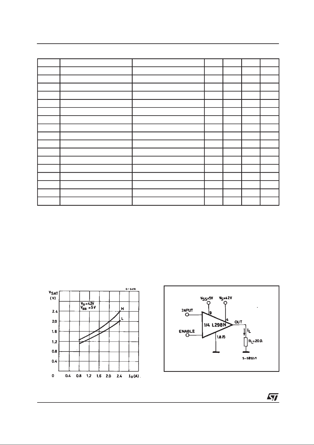
Figure1 : Typical SaturationVoltagevs.Output
Current.
min≥–0.5 V.
sens
Figure2 : SwitchingTimes TestCircuits.
4/13
Note : For INPUT Switching,set EN = H
For ENABLESwitching, set IN = H

L298
Figure3 :
Figure4 :
SourceCurrentDelayTimesvs. InputorEnable Switching.
SwitchingTimes Test Circuits.
Note : For INPUT Switching,set EN = H
ForENABLESwitching, set IN = L
5/13

L298
Figure5 :
SinkCurrent DelayTimes vs. Input 0 V EnableSwitching.
Figure6 : BidirectionalDC MotorControl.
Inpu ts Function
= H C = H ; D = L Forward
V
en
C = L ; D = H Reverse
C = D FastMotor Stop
= L C = X ; D = X FreeRunning
V
en
L = Low H =High X= Don’tcare
MotorStop
6/13

L298
Figure7 : Forhighercurrents,outputscanbe paralleled.Takecareto parallelchannel 1 with channel4
andchannel2 withchannel3.
APPLICATION INFORMATION (Refer to the block diagram)
1.1.POWEROUTPUT STAGE
TheL298integratestwopoweroutputstages(A;B).
The power output stage is a bridge configuration
and its outputscan drive an inductiveload in commonor differenzialmode,dependingonthestateof
the inputs. The currentthat flows through the load
comesoutfromthe bridgeat the sense output: an
externalresistor(R
SA;RSB
.)allowstodetectthein-
tensityof this current.
1.2.INPUT STAGE
Eachbridgeis drivenby meansof fourgatesthe in-
putof whichareIn1; In2 ; EnA and In3; In4 ; EnB.
TheIninputssetthebridgestatewhenTheEninput
ishigh;a lowstateoftheEninputinhibitsthebridge.
Alltheinputsare TTL compatible.
2.SUGGESTIONS
A non inductivecapacitor,usuallyof 100 nF, must
be foreseen between both Vs and Vss, to ground,
asnearaspossible toGNDpin.Whenthe largecapacitorof thepowersupply is too farfrom the IC, a
second smaller one must be foreseen near the
L298.
Thesenseresistor,not of a wirewoundtype, must
begroundednear thenegativepoleofVsthatmust
be nearthe GNDpin of the I.C.
Eachinput must be connectedto the source of the
driving signalsby meansof a veryshortpath.
Turn-OnandTurn-Off:BeforetoTurn-ONtheSupplyVoltageand beforetoTurnitOFF,theEnableinput mustbe drivento the Low state.
3.APPLICATIONS
Fig6 showsa bidirectionalDC motorcontrolSche-
maticDiagram forwhichonlyonebridgeisneeded.
Theexternalbridge of diodesD1 to D4 is made by
four fast recovery elements (trr
must be chosen of a VF as low as possibleat the
worstcase of the load current.
Thesenseoutputvoltagecanbeusedtocontrolthe
currentamplitudebychoppingtheinputs,or to provideovercurrentprotectionbyswitchinglow theenableinput.
The brake function (Fast motor stop) requires that
the Absolute Maximum Rating of 2 Amps must
neverbe overcome.
Whenthe repetitivepeak currentneededfrom the
loadis higher than 2 Amps,a paralleledconfigurationcan be chosen(See Fig.7).
An externalbridge of diodes are requiredwhen inductiveloadsare drivenandwhenthe inputsof the
ICarechopped;Shottkydiodeswouldbepreferred.
≤ 200 nsec) that
7/13

L298
Thissolutioncandriveuntil3 AmpsInDCoperation
anduntil3.5Amps of a repetitivepeakcurrent.
OnFig8itisshownthedrivingofa twophasebipolar
Fig 10 shows a secondtwo phasebipolar stepper
motorcontrolcircuit where the currentis controlled
bythe I.C.L6506.
steppermotor; the needed signalsto drive the inputs of the L298 are generated,in this example,
fromtheIC L297.
Fig9 showsan exampleof P.C.B. designedforthe
applicationofFig8.
Figure8 :
TwoPhase BipolarStepperMotorCircuit.
Thiscircuit drivesbipolar steppermotorswithwindingcurrentsup to 2 A. The diodesare fast2 A types.
RS1=RS2= 0.5
D1 to D8 = 2 A Fast diodes
8/13
Ω
VF≤ 1.2 V @ I = 2 A
{
trr≤200 ns

Figure9 : SuggestedPrintedCircuitBoardLayout for the Circuitof fig.8 (1:1scale).
L298
Figure10 : Two PhaseBipolar StepperMotorControlCircuitby UsingtheCurrent ControllerL6506.
RRand R
depend from the load current
sense
9/13

L298
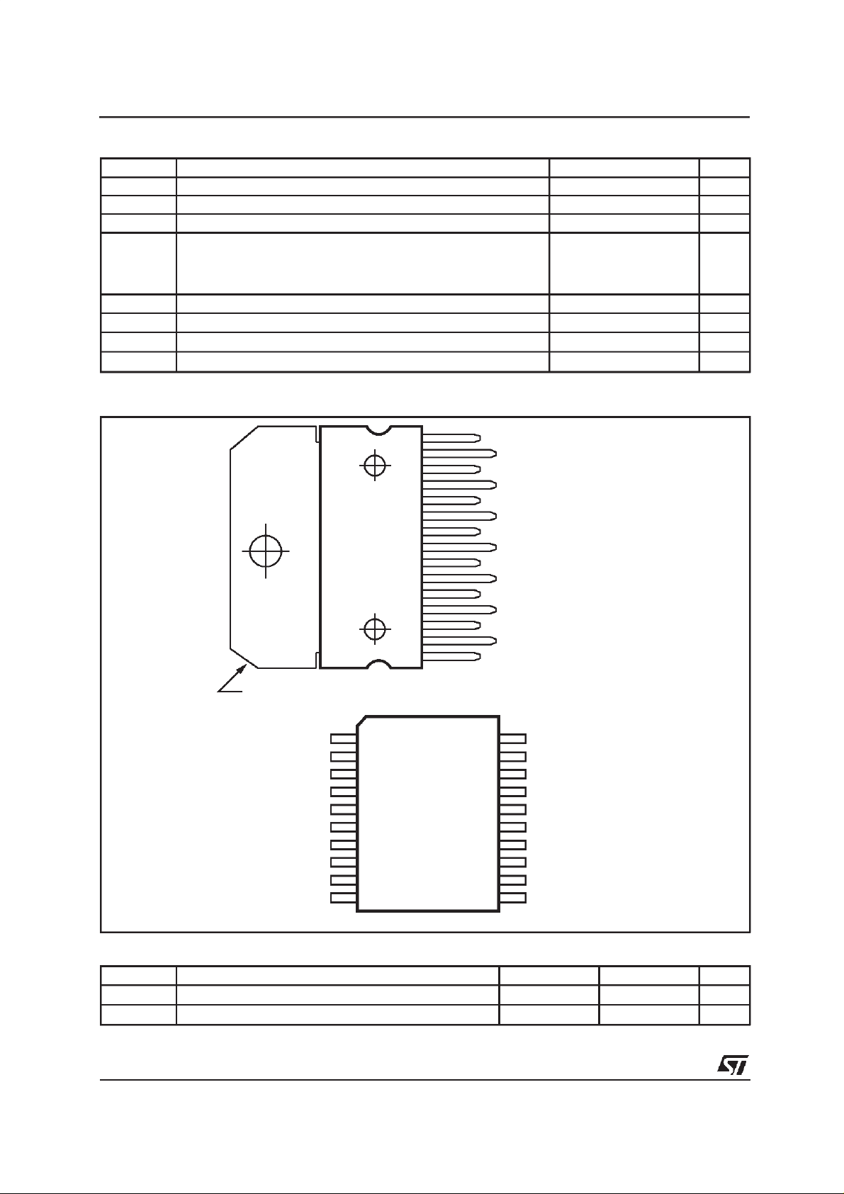
DIM.
MIN. TYP. MAX. MIN. TYP. MAX.
A5
B 2.65 0.104
C 1.6 0.063
D 1 0.039
E 0.49 0.55 0.019 0.022
F 0.66 0.75 0.026 0.030
G 1.02 1.27 1.52 0.040 0.050 0.060
G1 17.53 17.78 18.03 0.690 0.700 0.710
H1 19.6 0.772
H2 20.2 0.795
L 21.9 22.2 22.5 0.862 0.874 0.886
L1 21.7 22.1 22.5 0.854 0.870 0.886
L2 17.65 18.1 0.695
L3 17.25 17.5 17.75 0.679 0.689 0.699
L4 10.3 10.7 10.9 0.406 0.421 0.429
L7 2.65 2.9 0.104 0.114
M 4.25 4.55 4.85 0.167 0.179 0.191
M1 4.63 5.08 5.53 0.182 0.200 0.218
S 1.9 2.6 0.075 0.102
S1 1.9 2.6 0.075 0.102
Dia1 3.65 3.85 0.144 0.152
mm inch
0.197
0.713
OUTLINEAND
MECHANICALDATA
Multiwatt15 V
10/13

L298
DIM.
MIN. TYP. MAX. MIN. TYP. MAX.
A5
B 2.65 0.104
C 1.6 0.063
E 0.49 0.55 0.019 0.022
F 0.66 0.75 0.026 0.030
G 1.14 1.27 1.4 0.045 0.050 0.055
G1 17.57 17.78 17.91 0.692 0.700 0.705
H1 19.6 0.772
H2 20.2 0.795
L 20.57 0.810
L1 18.03
L2 2.54
L3 17.25 17.5 17.75 0.679 0.689
L4 10.3 10.7 10.9 0.406 0.421 0.429
L5 5.28 0.208
L6 2.38
L7 2.65 2.9 0.104 0.114
S 1.9 2.6 0.075 0.102
S1 1.9 2.6 0.075 0.102
Dia1 3.65 3.85 0.144 0.152
mm inch
0.197
0.710
0.100
0.699
0.094
OUTLINE AND
MECHANICAL DATA
Multiwatt15 H
11/13

L298
DIM.
MIN. TYP. MAX. MIN. TYP. MAX.
mm inch
A 3.6 0.142
a1 0.1 0.3 0.004
a2 3.3
0.012
0.130
a3 0 0.1 0.000 0.004
b 0.4 0.53 0.016 0.021
c 0.23 0.32 0.009 0.013
D (1) 15.8 16 0.622 0.630
D1 9.4 9.8 0.370 0.386
E 13.9 14.5 0.547 0.570
e 1.27 0.050
e3 11.43 0.450
E1 (1) 10.9 11.1 0.429 0.437
E2 2.9
0.114
E3 5.8 6.2 0.228 0.244
G 0 0.1 0.000 0.004
H 15.5 15.9 0.610 0.626
h 1.1
0.043
L 0.8 1.1 0.031 0.043
N10°(max.)
S
8°(max.)
T 10 0.394
(1) ”D andF” donot include moldflash or protrusions.
- Moldflash orprotrusions shall not exceed0.15 mm (0.006”).
- Criticaldimensions: ”E”, ”G” and ”a3”
OUTLINE AND
MECHANICAL DATA
JEDEC MO-166
PowerSO20
E2
hx
45
DETAIL B
BOTTOM VIEW
R
a3
Gage Plane
lead
E
DETAIL B
0.35
S
D1
a1
L
c
DETAIL A
slug
-C-
SEATING PLANE
GC
(COPLANARITY)
E3
NN
a2
A
b
DETAIL A
e3
H
D
T
1
e
1120
E1
10
PSO20MEC
12/13

L298
Information furnished is believed to be accurate and reliable. However, STMicroelectronics assumes no responsibility for the consequences of use of such information nor for any infringement of patents or other rights of third parties which may result from its use. No
license is granted by implication or otherwise under any patent or patent rights of STMicroelectronics. Specification mentioned in this
publication are subject to change without notice. This publication supersedes and replaces all information previously supplied. STMicroelectronics products are not authorized for use as critical components in life support devices or systems without express written
approval of STMicroelectronics.
Australia - Brazil - China - Finland - France - Germany - Hong Kong - India - Italy - Japan - Malaysia - Malta - Morocco -
The ST logo is a registered trademark of STMicroelectronics
2000 STMicroelectronics – Printed in Italy – All Rights Reserved
STMicroelectronics GROUP OF COMPANIES
Singapore - Spain - Sweden - Switzerland - United Kingdom - U.S.A.
http://www.st.com
13/13
 Loading...