

STEPPER MOTOR CONTROLLERS
NORMAL/WAWEDRIVE
HALF/FULLSTEP MODES
CLOCKWISE/ANTICLOCKWISEDIRECTION
SWITCHMODE LOAD CURRENT REGULA-
TION
PROGRAMMABLELOAD CURRENT
FEW EXTERNALCOMPONENTS
RESET INPUT & HOME OUTPUT
ENABLEINPUT
DIP20 SO20
ORDERING NUMBERS
:L297 (DIP20)
L297D (SO20)
L297
L297D
DESCRIPTION
The L297/A/D Stepper MotorController IC generates four phase drive signals fortwo phasebipolar
and four phase unipolar step motors in microcomputer-controlled applications. The motor can be
drivenin half step, normal and wawedrive modes
and on-chip PWM chopper circuits permit switchmode control of the current in the windings. A
featureof this device is that it requires only clock,
directionand modeinput signals.Since the phase
are generated internally the burden on the microprocessor,andtheprogrammer,is greatlyreduced.
Mounted in DIP20 and SO20 packages,the L297
can be used with monolithicbridge drives such as
the L298N or L293E, or with discrete transistors
and darlingtons.
ABSOLUTEMAXIMUMRATINGS
Symbol Parameter Value Unit
V
V
P
T
stg,Tj
Supply voltage 10 V
s
Input signals 7V
i
Totalpower dissipation (T
tot
Storage and junction temperature -40 to + 150 °
=70°C) 1 W
amb
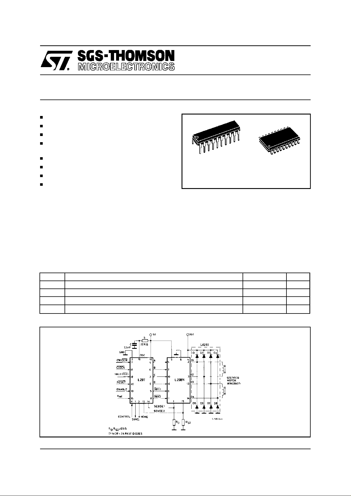
TWOPHASE BIPOLARSTEPPER MOTORCONTROL CIRCUIT
C
August 1996
1/11
L297-L297D
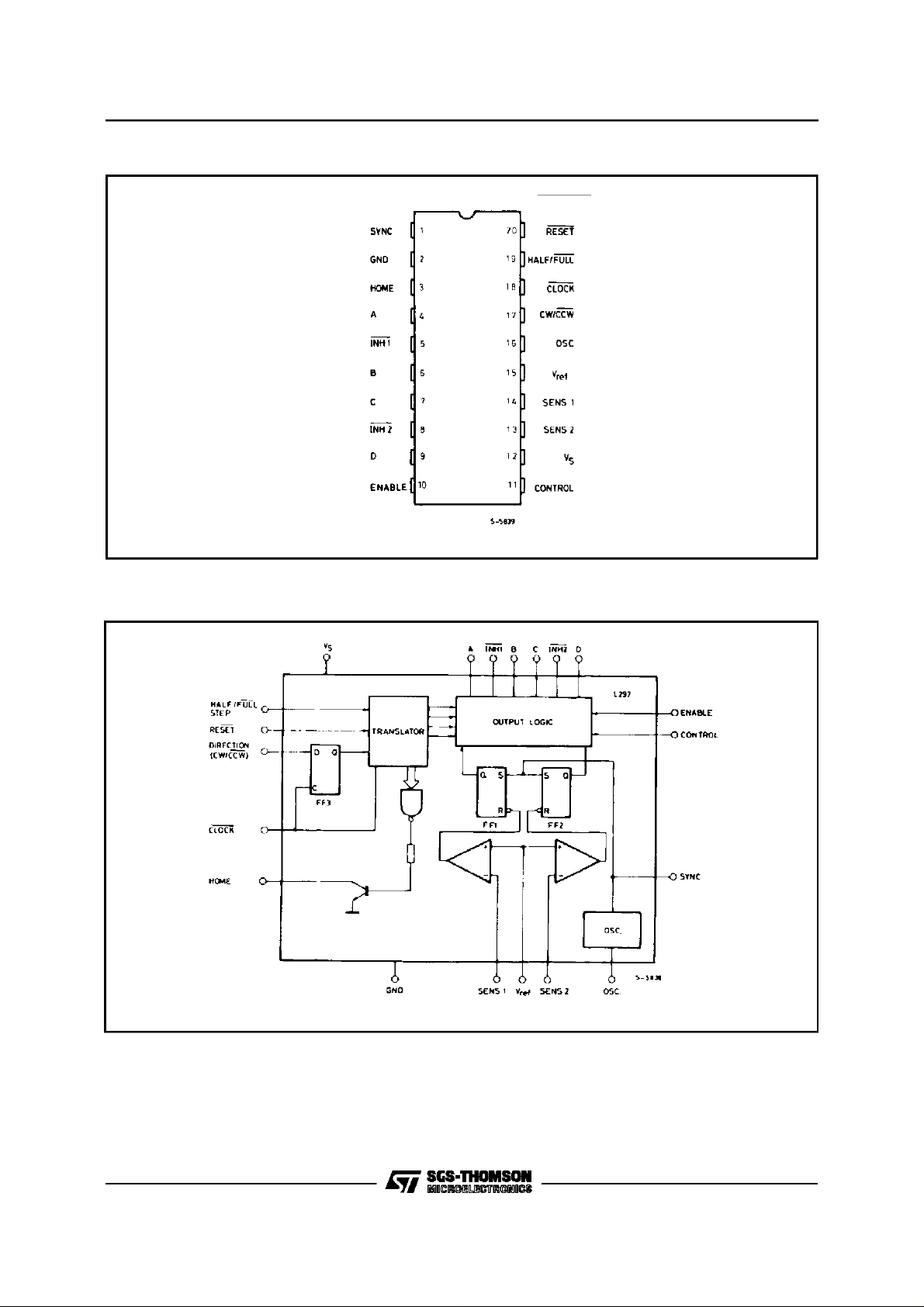
PIN CONNECTION (Topview)
L297
L297D
BLOCKDIAGRAM(L297/L297D)
2/11
PIN FUNCTIONS- L297/L297D
N° NAME FUNCTION
L297-L297D
1 SYNC Output of the on-chip chopper oscillator.
The SYNC connections The SYNC connectionsof all L297s to be
synchronized are connected together and the oscillator
components are omitted on all but one. If an external clock source
is used it is injected at this terminal.
2 GND Ground connection.
3 HOME Open collector output that indicates when the L297 is in its initial
state (ABCD = 0101).
The transistor is open when this signal is active.
4 A Motor phase A drive signal for powerstage.
5 INH1 Activelow inhibit control for driver stage of Aand B phases.
When a bipolar bridge is used this signal can be used to ensure
fastdecay of load current when a winding is de-energized.Also
used by chopper to regulate load current ifCONTROL input is low.
6 B Motor phase B drive signal for powerstage.
7 C Motor phase C drive signal forpower stage.
8 INH2 Activelow inhibit control for drive stages of C and D phases.
Same functions as INH1.
9 D Motor phase D drive signal forpower stage.
10 ENABLE Chip enable input. When low (inactive) INH1, INH2, A, B, C and D
are brought low.
11 CONTROL Control input that defines action of chopper.
When low chopper acts onINH1 and INH2; when high chopper
acts on phase lines ABCD.
12 V
s
13 SENS
2
5V supply input.
Input for load current sense voltage from power stages of phases
C and D.
14 SENS
1
Input for load current sense voltage from power stages of phases
A and B.
15 V
ref
16 OSC
Reference voltage for chopper circuit. A voltage applied to this pin
determines the peak load current.
An RC network (R to V
determines the chopper rate.This terminalis connected to ground
, C to ground) connected to this terminal
CC
on all butone device in synchronized multi - L297 configurations. f
1/0.69 RC
≅
17 CW/CCW Clockwise/counterclockwise direction control input.
Physical direction of motor rotation also dependson connection
of windings.
Synchronized internally thereforedirection can be changed at any
time.
18 CLOCK Stepclock. An activelow pulse on this input advances the motor
one increment. The step occurs on the rising edge of this signal.
3/11
L297-L297D
PIN FUNCTIONS- L297/L297D(continued)
N° NAME FUNCTION
19 HALF/FULL Half/full step selectinput. When high selects half step operation,
20 RESET Reset input. An active low pulse on this input restores the
when low selects full step operation. One-phase-on full step mode
is obtained by selecting FULL when the L297’stranslator is at an
even-numbered state.
Two-phase-on full step mode is set by selecting FULL when the
translator is at an odd numbered position. (The home position is
designate state 1).
translator to thehome position (state 1, ABCD= 0101).
THERMALDATA
Symbol Parameter DIP20 SO20 Unit
R
th-j-amb
CIRCUITOPERATION
The L297 is intended for use with a dual bridge
driver, quad darlington array or discrete power
devices in step motor driving applications. It re-
Thermal resistance junction-ambient max 80 100 °
arechoppedthe non-activephase line of eachpair
(ABor CD)is activated(ratherthan interruptingthe
linethen active).InL297 +L298 configurationsthis
technique reduces dissipation in the load current
senseresistors.
ceivesstep clock,directionand mode signals from
the systems controller (usually a microcomputer
chip) and generates control signals for the power
stage.
Theprincipalfunctionsare a translator,whichgenerates the motor phase sequences, and a dual
PWMchoppercircuit whichregulatesthecurrentin
themotorwindings.The translatorgeneratesthree
different sequences, selected by the HALF/FULL
input. These are normal (two phases energised),
wave drive (one phase energised) and half-step
(alternately one phase energised/two phases energised).Twoinhibit signals are also generated by
theL297in half stepand wavedrivemodes.These
signals,whichconnectdirectlyto the L298’senable
inputs, are intended to speed current decay when
a winding is de-energised.When the L297 is used
todrivea unipolarmotorthe chopper actson these
lines.
Aninputcalled CONTROLdetermineswhetherthe
A common on-chip oscillator drivesthe dual chopper.It suppliespulsesat thechopperratewhichset
thetwoflip-flopsFF1 and FF2.Whenthe currentin
awindingreachesthe programmedpeakvaluethe
voltage across the sense resistor (connected to
one of the sense inputs SENS
and the corresponding comparator resets its
V
ref
or SENS2) equals
1
flip flop,interrupting the drive currentuntil the next
oscillator pulse arrives. The peak current for both
windingsis programmedbya voltagedivideron the
input.
V
ref
Ground noise problems in multiple configurations
can be avoidedby synchronisingthe chopper oscillators.This is done by connecting all the SYNC
pins together,mounting the oscillator RC network
on one device only andgrounding the OSC pin on
all other devices.
chopper will act on the phase lines ABCD or the
inhibitlines INH1 and INH2.When the phaselines
C/W
4/11

MOTORDRIVING PHASE SEQUENCES
The L297’s translator generatesphase sequences
for normal drive, wave drive and half step modes.
The state sequences and output waveforms for
these three modes are shown below. In all cases
Clockwise rotation is indicate;for anticlockwiserotation the sequences are simply reversed RESET
restores the translator to state 1, where ABCD =
0101.
the translator advanceson the low to high transistion of CLOCK.
HALF STEP MODE
Half step mode is selectedbya high levelon the HALF/FULL input.
L297-L297D
NORMALDRIVE MODE
Normal drive mode (also called ”two-phase-on” drive) is selected by a low level on the HALF/FULL input
when the translator is at an odd numbered state (1, 3, 5 or 7). In this mode the INH1 and INH2 outputs
remain high throughout.
5/11

L297-L297D
MOTORDRIVING PHASE SEQUENCES(continued)
WAVE DRIVE MODE
Wave drive mode (also called ”one-phase-on” drive) is selected by a low level on the HALF/FULL input
when the translatoris at an evennumbered state (2, 4, 6 or 8).
ELECTRICALCHARACTERISTICS
(Refer to the blockdiagram T
=25°C, Vs= 5V unless otherwise
amb
specified)
Symbol Parameter Testconditions Min. Typ Max. Unit
Supply voltage (pin 12) 4.75 7 V
V
s
Quiescent supply current (pin 12) Outputs floating 50 80 mA
I
s
Input voltage
V
i
(pin 11, 17, 18, 19, 20)
Input current
I
i
(pin 11, 17, 18, 19, 20)
V
Enable input voltage(pin 10) Low 1.3 V
en
Enable input current(pin 10)
I
en
Phase output voltage
V
o
Io= 10mA V
(pins 4, 6, 7, 9)
= 5mA V
I
o
V
Inhibit output voltage (pins 5, 8) Io= 10mA V
inh
Low 0.6 V
High 2 V
V
= L 100 µ
i
=H 10
V
i
High 2 V
= L 100 µ
V
en
=H 10 µ
V
en
OL
OH
inh L
3.9 V
s
A
s
0.4 V
0.4 V
V
A
µ
V
A
A
V
6/11
SYNC
= 5mA V
I
o
Sync OutputVoltage Io= 5mA V
= 5mA V
I
o
inh H
SYNC H
SYNC V
3.9 V
3.3 V
0.8

L297-L297D
ELECTRICALCHARACTERISTICS
(continued)
Symbol Parameter Testconditions Min. Typ Max. Unit
I
V
V
Leakage current (pin 3) VCE=7V 1 µ
leak
Saturation voltage (pin 3) I = 5 mA 0.4 V
sat
Comparators offset voltage
off
(pins 13, 14, 15)
I
Comparator bias current
o
V
=1V 5 mV
ref
-100 10
(pins 13, 14, 15)
V
t
t
RCLK
Input reference voltage (pin 15) 0 3 V
ref
Clock time 0.5 µ
CLK
Set up time 1
t
S
Hold time 4
t
H
Reset time 1
t
R
Reset to clock delay 1 µ
µ
µs
µs
µ
A
A
s
s
s
Figure1.
7/11

L297-L297D
APPLICATION INFORMATION
TWOPHASEBIPOLAR STEPPERMOTORCONTROLCIRCUIT
This circuitdrives bipolar stepper motors with winding currentsup to 2A.The diodesare fast 2A types.
Figure2.
Figure3 :SynchronisingL297s
8/11

DIP20 PACKAGEMECHANICAL DATA
L297-L297D
DIM.
MIN. TYP. MAX. MIN. TYP. MAX.
a1 0.254 0.010
B 1.39 1.65 0.055 0.065
b 0.45 0.018
b1 0.25 0.010
D 25.4 1.000
E 8.5 0.335
e 2.54 0.100
e3 22.86 0.900
F 7.1 0.280
I 3.93 0.155
L 3.3 0.130
Z 1.34 0.053
mm inch
9/11

L297-L297D
SO20 PACKAGEMECHANICAL DATA
DIM.
MIN. TYP. MAX. MIN. TYP. MAX.
A 2.65 0.104
a1 0.1 0.3 0.004 0.012
a2 2.45 0.096
b 0.35 0.49 0.014 0.019
b1 0.23 0.32 0.009 0.013
C 0.5 0.020
c1 45 (typ.)
D 12.6 13.0 0.496 0.512
E 10 10.65 0.394 0.419
e 1.27 0.050
e3 11.43 0.450
F 7.4 7.6 0.291 0.299
L 0.5 1.27 0.020 0.050
M 0.75 0.030
mm inch
S 8 (max.)
10/11

L297-L297D
Information furnished is believed to be accurate and reliable. However, SGS-THOMSON Microelectronics assumes no responsibility for the
consequences of use of such information nor for any infringement of patents or other rights of third parties which may result from its use. No
license is granted by implication or otherwise under any patentor patent rights of SGS-THOMSON Microelectronics. Specification mentioned
in this publication are subject to change without notice. This publication supersedes and replaces all information previously supplied.
SGS-THOMSONMicroelectronics products are not authorizedfor useas critical componentsin lifesupport devicesor systems without express
written approval of SGS-THOMSON Microelectronics.
1996 SGS-THOMSON Microelectronics – Printed in Italy – All Rights Reserved
SGS-THOMSON Microelectronics GROUP OF COMPANIES
Australia - Brazil - Canada - China - France- Germany - Hong Kong - Italy- Japan - Korea- Malaysia - Malta - Morocco - The Netherlands -
Singapore - Spain- Sweden - Switzerland - Taiwan - Thailand - UnitedKingdom- U.S.A.
11/11
 Loading...