

L297
L297A
STEPPER MOTOR CONTROLLERS
NORMAL/WAWEDRIVE
HALF/FULLSTEP MODES
CLOCKWISE/ANTICLOCKWISEDIRECTION
SWITCHMODE LOAD CURRENT REGULA-
TION
PROGRAMMABLE LOAD CURRENT
FEWEXTERNALCOMPONENTS
RESETINPUT& HOME OUTPUT
ENABLEINPUT
STEP-PULSEDOUBLER(L297Aonly)
DESCRIPTION
The L297 Stepper Motor Controller IC generates
fourphase drivesignals for two phase bipolar and
fourphaseunipolar stepmotorsinmicrocomputercontrolledapplications.The motor can be driven in
half step, normal and wawe drive modes and onchip PWM chopper circuits permit switch-mode
control of thecurrent in the windings. A feature of
October 1991
Symbol Parameter Value Unit
V
s
Supply voltage 10 V
V
i
Input signals 7V
P
tot
Totalpower dissipation (T
amb
=70°C)
1W
T
stg,Tj
Storage and junction temperature -40 to + 150 °C
ABSOLUTEMAXIMUM RATINGS
this device is that it requires only clock, direction
and mode input signals. Sincethe phaseare generated internallytheburdenonthemicroprocessor,
and the programmer,is greatly reduced. Mounted
in a 20-pin plastic package, the L297 canbe used
with monolithicbridge drivessuch asthe L298N or
L293E, orwith discretetransistorsanddarlingtons.
The L297Aalso includesa clock pulse doubler.
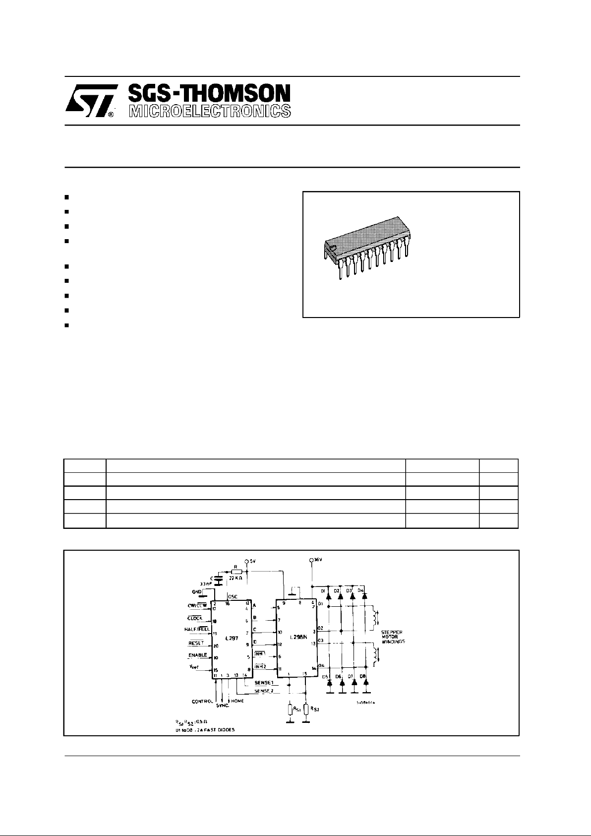
TWOPHASE BIPOLAR STEPPER MOTOR CONTROL CIRCUIT
DIP-20 Plastic
(0.25)
ORDER CODES : L297 - L297A
1/11
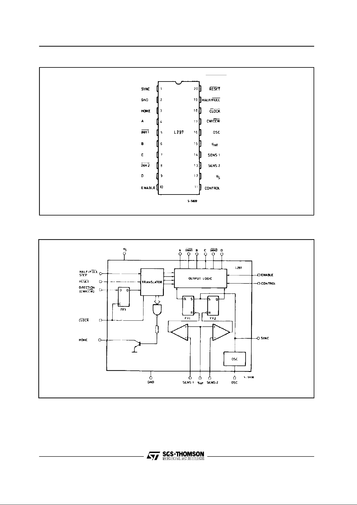
PIN CONNECTION (L297)
BLOCK DIAGRAM (L297)
2/11
L297-L297A
Symbol Parameter Value Unit
Rth-j-amb Thermal resistance junction-ambient max 80 °C/W
THERMALDATA
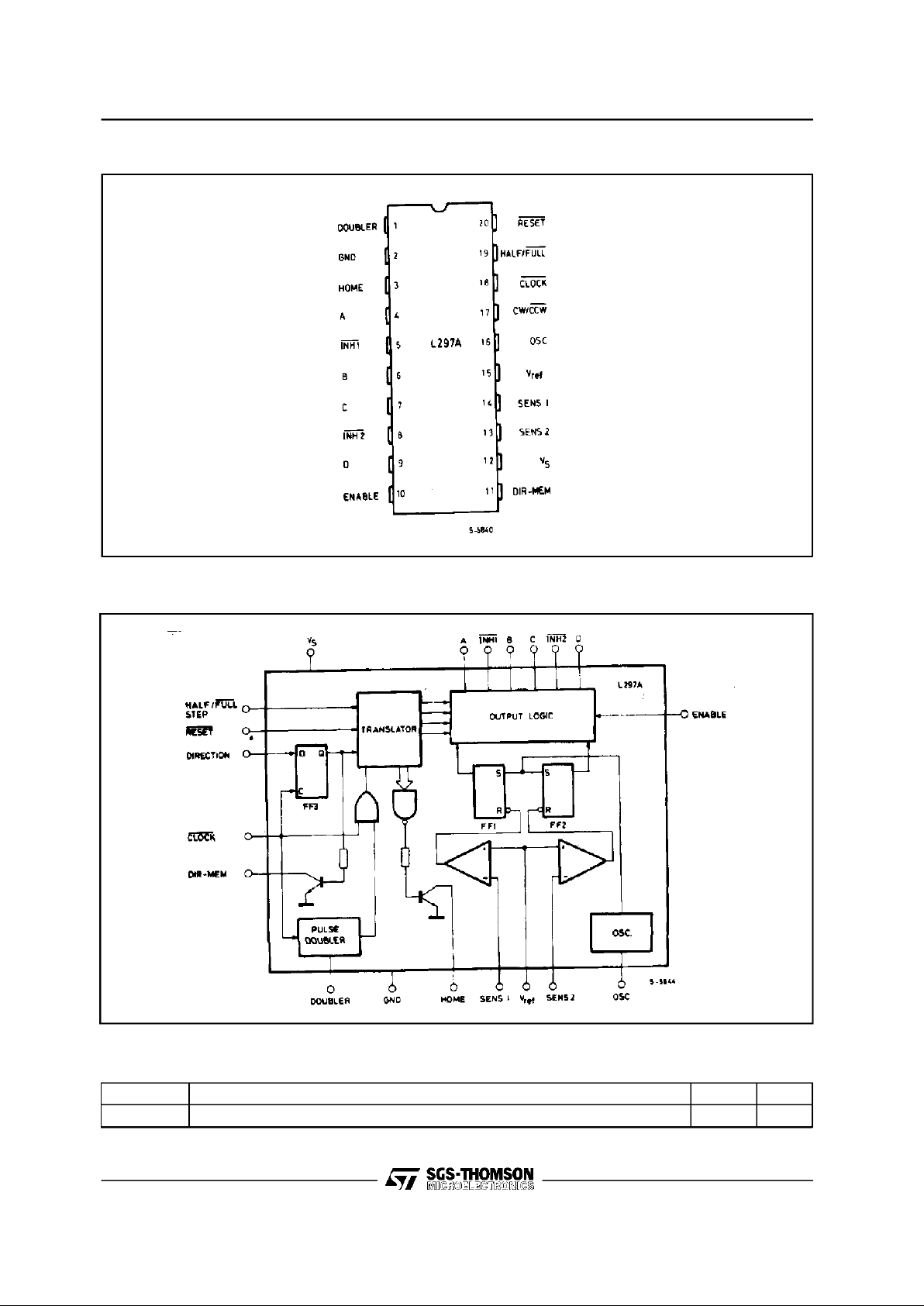
BLOCK DIAGRAM (L297A)
PIN CONNECTION (L297A)
3/11
L297-L297A
4/11
N°
NAME FUNCTION
1 SYNC Output of the on-chip chopper oscillator.
TheSYNC connections The SYNC connections of all L297s to be
synchronized are connected together and the oscillator
componentsare omitted on all but one. If an external clock
source is used it is injected at this terminal.
2 GND Ground connection.
3 HOME Open collector output that indicates when the L297 is in itsinitial
state (ABCD = 0101).
Thetransistor is open when this signal is active.
4 A Motor phase Adrive signal for power stage.
5 INH1 Activelow inhibit control for driverstage of Aand B phases.
When a bipolar bridge isused this signal can be used to ensure
fast decay of load current when a winding is de-energized. Also
used by chopper to regulate load current if CONTROL input is low.
6 B Motor phase B drive signal for power stage.
7 C Motorphase C drive signal for power stage.
8 INH2 Activelow inhibit control for drive stages of C and D phases.
Same functions as INH1.
9 D Motorphase D drive signal for power stage.
10 ENABLE Chipenable input. When low (inactive) INH1, INH2, A, B,C and D
are brought low.
11 CONTROL Controlinput that defines action of chopper.
When low chopper acts on INH1 and INH2;when high chopper
acts on phase lines ABCD.
12 V
s
5Vsupply input.
13 SENS
2
Inputfor load current sense voltage from power stagesof phases
C and D.
14 SENS
1
Inputfor load current sense voltage from power stagesof phases
Aand B.
15 V
ref
Reference voltage for chopper circuit. Avoltage applied to this pin
determinesthe peak load current.
16 OSC
AnRC network (R to V
CC
, C to ground) connected to this terminal
determinesthe chopper rate. This terminal is connected to
groundon all but one device in synchronized multi - L297
configurations. f ≅ 1/0.69 RC
17 CW/CCW Clockwise/counterclockwise direction control input.
Physical direction of motor rotation also depends on connection
of windings.
Synchronized internally therefore direction can be changed at any
time.
18 CLOCK Stepclock. An activelow pulse on this input advances the motor
one increment. The step occurs on the rising edge of this signal.
PIN FUNCTIONS - L297
L297-L297A

N°
NAME FUNCTION
19 HALF/FULL Half/full step select input. When high selects halfstep operation,
whenlow selects fullstep operation. One-phase-on full step
mode is obtained by selecting FULL when the L297’s translator is
at an even-numbered state.
Two-phase-on full step mode is set by selecting FULL when the
translator is at an odd numbered position. (The home position is
designate state 1).
20 RESET Reset input. An active low pulse on this input restores the
translator to the home position (state 1, ABCD = 0101).
PIN FUNCTIONS - L297 (continued)
N° NAME FUNCTION
1 DOUBLER An RC network connected to this pin determines the delay
betweenan input clock pulse and thecorresponding ghost pulse.
11 DIR-MEM Direction Memory. Inverted output of the direction flip flop. Open
collector output.
PIN FUNCTIONS - L297A
Pin functionof the L297Aare identicalto those of the L297 except for pins 1 and 11.
CIRCUIT OPERATION
The L297(A)is intendedfor use with a dual bridge
driver,quad darlington array or discrete power devices in step motor driving applications.It receives
step clock, direction and mode signals from the
systems controller (usually a microcomputer chip)
and generates control signals for the powerstage.
The principalfunctions are a translator, which generates the motor phase sequences, and a dual
PW/M chopper circuit which regulates the current
in the motor windings. The translator generates
t hr ee d iffer en t sequen ce s, sele cted by t h e
HALF/FULLinput. These are normal (two phases
energised),wave drive (one phase energised)and
half-step (alternately one phase energised/two
phases energised). Two inhibit signals are also
generatedby the L297 in half step andwave drive
modes.Thesesignals,whichconnectdirectlytothe
L298’senableinputs,areintendedtospeedcurrent
decay when a winding is de-energised.When the
L297 is used to drivea unipolarmotor the chopper
acts onthese lines.
An inputcalledCONTROLdetermineswhetherthe
chopper will act on the phase lines ABCD or the
inhibitlines INH1 and INH2. When the phase lines
are choppedthe non-activephase line of eachpair
(AB or CD) isactivated(rather than interruptingthe
line then active).In L297 + L298 configurationsthis
technique reduces dissipation in the load current
sense resistors.
A common on-chip oscillator drives the dual chopper.It suppliespulses atthe chopperrate which set
the twoflip-flops FF1 andFF2. When the currentin
a windingreaches the programmedpeak valuethe
voltageacrossthe senseresistor(connectedtoone
of the sense inputs SENS
1
or SENS2) equalsV
ref
and the corresponding comparator resets its flip
flop, interrupting the drive current until the next
oscillator pulse arrives. The peak current for both
windingsis programmedbya voltagedivideron the
V
ref
input.
Ground noise problems in multiple configurations
can be avoidedby synchronisingthechopperoscillators.This isdoneby connectingallthe SYNCpins
together, mounting the oscillator RC network on
one deviceonly and grounding the OSC pin on all
other devices.
The L297A includes a pulse doubler on the step
clock line which is intendedto simplify the implementation of multiple stepping. A ghost pulse is
generatedautomaticallyaftereachinputpulse, delayed by the time 0.75 R
dCd
.
The RC network should be dimensioned to place
the ghost pulse roughly halfway between clock
pulses.Ifpin1 (DOUBLER)is groundedthedoubler
functionis disabled.
5/11
L297-L297A

6/11
MOTORDRIVINGPHASE SEQUENCES
The L297’s translator generatesphase sequences
for normal drive, wave drive and half step modes.
The state sequences and output waveforms for
these three modes are shown below. In all cases
the translator advances on the low to high transistion of CLOCK.
Clockwise rotation is indicate;for anticlockwiserotation the sequences are simply reversed RESET
restores the translator to state 1, where ABCD =
0101.
HALF STEP MODE
Half stepmode is selected by a high level on the HALF/FULLinput.
NORMALDRIVE MODE
Normal drive mode (also called ”two-phase-on” drive) is selected by a low level on the HALF/FULL input
when the translator is at an odd numbered state (1, 3, 5 or 7). In this mode the INH1 and INH2 outputs
remain high throughout.
L297-L297A

MOTORDRIVINGPHASE SEQUENCES (continued)
WAVEDRIVE MODE
Wave drive mode (also called ”one-phase-on” drive) is selected by a low level on the HALF/FULL input
when the translator is at an even numbered state (2, 4, 6 or 8).
Symbol Parameter Testconditions Min. Typ Max. Unit
V
s
Supply voltage (pin 12) 4.75 7 V
I
s
Quiescent supply current (pin 12) Outputs floating 50 80 mA
V
i
Input voltage
(pin 11, 17, 18,19, 20)
Low 0.8 V
High 2 V
s
V
I
i
Input current
(pin 11, 17, 18,19, 20)
Vi= L 100 µ
A
V
i
=H 10 µA
V
en
Enable input voltage (pin 10) Low 1.5 V
High 2 V
s
V
I
en
Enable input current (pin 10)
V
en
= L 100 µ
A
V
en
=H 10 µA
V
o
Phase output voltage
(pins 4, 6, 7, 9)
Io= 10mA V
OL
0.4 V
I
o
= 5mA V
OH
3.9 V
V
inh
Inhibit output voltage (pins 5, 8) Io= 10mA V
inh L
0.4 V
I
o
= 5mA V
inh H
3.9 V
V
SYNC
Sync Output Voltage Io= 5mA V
SYNC H
3.3 V
I
o
= 5mA V
SYNC V
0.8
ELECTRICAL CHARACTERISTICS (Refer to the block diagram T
amb
=25°C, Vs= 5V unless otherwise
specified)
7/11
L297-L297A

8/11
Symbol Parameter Test conditions Min. Typ Max. Unit
I
leak
Leakage current (pin 3, 11*) VCE=7V 1
µA
V
sat
Saturation voltage (pins 3, 11*) I = 5 mA 0.4 V
V
off
Comparators offset voltage
(pins 13, 14, 15)
V
ref
=1V 5 mV
I
o
Comparator bias current
(pins 13, 14, 15)
-100 10
µA
V
ref
Input reference voltage(pin 15) 0 3 V
t
CLK
Clock time 0.5 µ
s
t
S
Set up time 1
µs
t
H
Hold time 4
µs
t
R
Reset time 1 µs
t
RCLK
Reset to clock delay 1 µs
ELECTRICALCHARACTERISTICS (continued)
* L297Aonly
Figure 1.
L297-L297A

APPLICATIONINFORMATION
TWOPHASE BIPOLARSTEPPER MOTORCONTROLCIRCUIT
This circuit drives bipolar stepper motors with winding currents up to 2A. The diodes are fast 2A types.
Figure2.
Figure3 : SynchronisingL297s Figure4 : Pulse doubler (L297A)
9/11
L297-L297A

10/11
DIM.
mm inch
MIN. TYP. MAX. MIN. TYP. MAX.
a1 0.254 0.010
B 1.39 1.65 0.055 0.065
b 0.45 0.018
b1 0.25 0.010
D 25.4 1.000
E 8.5 0.335
e 2.54 0.100
e3 22.86 0.900
F 7.1 0.280
I 3.93 0.155
L 3.3 0.130
Z 1.34 0.053
DIP20 PACKAGE MECHANICALDATA
L297-L297A

Information furnished is believed to be accurate and reliable. However, SGS-THOMSON Microelectronics assumes no responsibility for the
consequences of use of such information nor for any infringement of patents or other rights of third parties which may result from its use. No
licenseis granted by implication or otherwise under any patent or patent rights of SGS-THOMSON Microelectronics. Specifications mentioned
in this publication are subject to change without notice. This publication supersedes and replaces all information previously supplied.
SGS-THOMSON Microelectronics products are not authorized foruse as critical componentsin life supportdevices or systems without express
written approval of SGS-THOMSON Microelectronics.
1994 SGS-THOMSON Microelectronics - AllRights Reserved
SGS-THOMSON Microelectronics GROUP OF COMPANIES
Australia - Brazil -France - Germany - Hong Kong - Italy - Japan - Korea - Malaysia -Malta - Morocco - The Netherlands - Singapore -
Spain - Sweden - Switzerland - Taiwan- Thaliand - United Kingdom - U.S.A.
11/11
L297-L297A
 Loading...