

Page 1
L296
L296P
April1993
HIGH CURRENT SWITCHING REGULATORS
.4 A OUTPUT CURRENT
.5.1 V TO 40 V OUTPUT VOLTAGERANGE
.0 TO 100 % DUTY CYCLERANGE
.PRECISE(±2 %) ON-CHIPREFERENCE
.SWITCHINGFREQUENCYUP TO200KHz
.VERY HIGHEFFICIENCY(UPTO 90%)
.VERY FEWEXTERNAL COMPONENTS
.SOFT START
.RESETOUTPUT
.EXTERNALPROGRAMMABLE LIMITING
CURRENT (L296P)
.CONTROLCIRCUITFOR CROWBAR SCR
.INPUT FOR REMOTE INHIBIT AND
SYNCHRONUSPWM
.THERMALSHUTDOWN
DESCRIP TION
TheL296andL296Parestepdownpowerswitching
regulatorsdelivering4 Aat a voltage variablefrom
5.1 Vto40 V.
Featuresof thedevicesincludesoftstart,remotein-
hibit, thermal protection, a reset output for microprocessors and a PWM comparatorinput for synchronizationin multichip configurations.
TheL296Pincudesexternalprogrammablelimiting
current.
TheL296 andL296Paremountedina15-leadMultiwattplasticpowerpackageandrequiresveryfew
externalcomponents.
Efficient operation at switching frequencies up to
200 KHz allows a reductionin the size and costof
external filter components. A voltage sense input
and SCR drive output are provided for optional
crowbar overvoltage protection with an external
SCR.
Multiwatt
(15 lead)
ORDE RING NUM BERS :
L296 (Vertical) L296HT (Hor izontal)
L296P ( Vertical) L296PHT ( H ori zont a l)
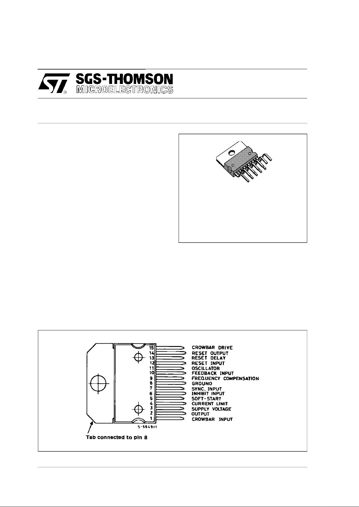
PIN CONNE CTION (top view)
1/21
Page 2
PIN FUNCTIONS
N° Name Function
1 CROWBAR INPUT Voltage Sense Input for Crowbar Overvoltage Protection. Normally connected to the
feedback input thus triggering the SCR when V
out
exceeds nominal by 20 %. May
also monitor the input and a voltage divider can be added to increase the threshold.
Connected to ground when SCR not used.
2 OUTPUT Regulator Output
3 SUPPLY VOLTAGE Unrergulated Voltage Input. An internal Regulator Powers the L296s Internal Logic.
4 CURRENT LIMIT A resistor connected between this terminal and ground sets the current limiter
threshold. If this terminal is left unconnected the threshold is internally set (see
electrical characteristics).
5 SOFT START Soft Start Time Constant. A capacitor is connected between this terminal and ground
to define the soft start time constant. This capacitor also determines the average
short circuit output current.
6 INHIBIT INPUT TTL – Level Remote Inhibit. A logic high level on this input disables the device.
7 SYNC INPUT Multiple L296s are synchronized by connecting the pin 7 inputs together and omitting
the oscillator RC network on all but one device.
8 GROUND Common Ground Terminal
9 FREQUENCY
COMPENSATION
A series RC network connected between this terminal and ground determines the
regulation loop gain characteristics.
10 FEEDBACK INPUT The Feedback Terminal on the Regulation Loop. The output is connected directly to
this terminal for 5.1V operation ; it is connected via a divider for higher voltages.
11 OSCILLATOR A parallel RC networki connected to this terminal determines the switching frequency.
This pin must be connected to pin 7 input when the internal oscillator is used.
12 RESET INPUT Input of the Reset Circuit. The threshold is roughly 5 V. It may be connected to the
feedback point or via a divider to the input.
13 RESET DELAY A capacitor connected between this terminal and ground determines the reset signal
delay time.
14 RESET OUTPUT Open collector reset signal output. This output is high when the supply is safe.
15 CROWBAR OUTPUT SCR gate drive output of the crowbar circuit.
BLOCK DIAGRAM
L296 - L296P
2/21
Page 3
CIRCUIT OPERATION
(refer to the block diagram)
The L296 and L296P are monolithic stepdown
switchingregulatorsprovidingoutputvoltagesfrom
5.1Vto40Vand delivering 4A.
Theregulationloopconsistsofasawtoothoscillator,
erroramplifier,comparatorandtheoutputstage.An
error signal is produced by comparing the output
voltagewitha precise5.1Von-chipreference(zener
zaptrimmedto± 2%).Thiserrorsignalis thencomparedwiththesawtoothsignalto generatethefixed
frequencypulsewidthmodulatedpulseswhichdrive
theoutputstage.Thegainandfrequencystabilityof
theloopcanbeadjustedbyan externalRC network
connectedtopin9.Closingtheloopdirectlygivesan
outputvoltageof5.1V.Highervoltagesareobtained
byinsertinga voltagedivider.
Outputovercurrentsat switchon are preventedby
the soft start function. The error amplifier outputis
initially clampedby the externalcapacitorCss and
allowedtorise, linearly,as thiscapacitorischarged
bya constantcurrentsource.
Outputoverloadprotectionis providedintheformof
a currentlimiter. The load currentis sensed by an
internalmetal resistor connectedto a comparator.
Whenthe load current exceedsa preset threshold
this comparator sets a flip flop which disables the
outputstageanddischargesthesoftstartcapacitor.
A second comparator resets the flip flop when the
voltageacrossthe soft startcapacitorhas fallen to
0.4V.The output stage is thus re-enabled and the
output voltage rises under control of the soft start
network.If theoverloadconditionis stillpresentthe
limiterwill triggeragainwhen the thresholdcurrent
isreached.The averageshort circuit current islimitedtoa safe valueby the deadtimeintroduced by
the softstart network.
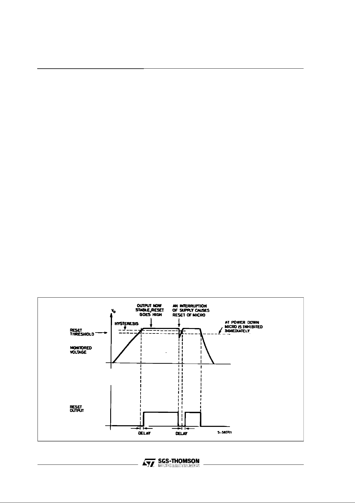
The reset circuit generatesan output signal when
the supply voltage exceeds a threshold programmed byan externaldivider.The resetsignalis
generatedwitha delay timeprogrammedby an external capacitor. When the supply falls below the
threshold the reset output goes low immediately.
Theresetoutputis an opencollector.
Thescrowbarcircuit sensestheoutput voltageand
the crowbaroutputcan providea currentof 100mA
toswitchon anexternalSCR. ThisSCRis triggered
when the output voltage exceeds the nominal by
20%. There is no internalconnection between the
outputandcrowbarsense inputthereforethe crowbar canmonitor eitherthe input or the output.
ATTL-levelinhibitinputisprovidedforapplications
suchasremoteon/offcontrol.Thisinputisactivated
byhigh logiclevelanddisablescircuitoperation.After an inhibit the L296 restartsunder controlof the
soft startnetwork.
Thethermaloverloadcircuit disablescircuit operation when the junctiontemperaturereachesabout
150 °Candhas hysteresisto preventunstablecon-
ditions.
Figure 1 : ResetOutput Waveforms
L296 - L296P
3/21
Page 4
Figure 2 : SoftStartWaveforms
Figure 3 : CurrentLimiter Waveforms
ABSOLUTE MAXIMUM RATINGS
Symbol Parameter Value Unit
V
i
Input Voltage (pin 3) 50 V
V
i–V2
Input to Output Voltage Difference 50 V
V
2
Output DC Voltage
Output Peak Voltage at t = 0.1 µsec f = 200KHz
–1
–7
V
V
V
1,V12
Voltage at Pins 1, 12 10 V
V
15
Voltage at Pin 15 15 V
V
4,V5,V7,V9,V13
Voltage at Pins 4, 5, 7, 9 and 13 5.5 V
V
10,V6
Voltage at Pins 10 and 6 7 V
V
14
Voltage at Pin 14 (I14≤ 1 mA) V
i
I
9
Pin 9 Sink Current 1 mA
I
11
Pin 11 Source Current 20 mA
I
14
Pin 14 Sink Current (V14< 5 V) 50 mA
P
tot
Power Dissipation at T
case
≤ 90 °C20W
T
j
,T
stg
Junction and Storage Temperature – 40 to 150 °C
L296 - L296P
4/21
Page 5
THERMAL DATA
Symbol Parameter Value Unit
R
th j-case
Thermal Resistance Junction-case Max. 3 °C/W
R
th j-amb
Thermal Resistance Junction-ambient Max. 35 °C/W
ELECTRICAL CHARACTERISTICS
(refer to the test circuits T
j
=25oC, Vi= 35V, unless otherwise specified)
Symbol Parameter Test Conditions Min. Typ. Max. Unit Fig.
DYNAMIC CHARACTERISTICS (pin 6 to GND unless otherwise specified)
V
o
Output Voltage Range Vi= 46V, Io=1A V
ref
40 V 4
V
i
Input Voltage Range Vo=V
ref
to 36V, Io≤ 3A 9 46 V 4
V
i
Input Voltage Range Note (1), Vo=V
REF
to 36V Io=4A 46 V 4
∆V
o
Line Regulation Vi=10V to 40V, Vo=V
ref,Io
=2A 15 50 mV 4
∆V
o
Load Regulation Vo=V
ref
Io=2Ato4A
I
o
= 0.5A to 4A
101530
45
mV 4
V
ref
Internal Reference Voltage (pin 10) Vi= 9V to 46V, Io= 2A 5 5.1 5.2 V 4
∆ V
ref
∆ T
Average Temperature Coefficient
of Reference Voltage
T
j
=0°C to 125°C, Io= 2A 0.4 mV/°C
V
d
Dropout Voltage Between Pin 2
and Pin 3
Io=4A
I
o
=2A
2
1.3
3.2
2.1
V
V
4
4
I
2L
Current Limiting Threshold (pin 2) L296 - Pin 4 Open,
V
i
= 9V to 40V, Vo=V
ref
to 36V
4.5 7.5 A 4
L296P - V
i
= 9V to 40V, Vo=V
ref
Pin 4 Open
R
Iim
= 22kΩ
5
2.5
7
4.5
A4
I
SH
Input Average Current Vi= 46V, Output Short-circuited 60 100 mA 4
η Efficiency I
o
=3A
V
o=Vref
Vo= 12V
75
85
%4
SVR Supply Voltage Ripple Rejection ∆V
i
=2V
rms,fripple
= 100Hz
V
o=Vref,Io
=2A
50 56 dB 4
f Switching Frequency 85 100 115 kHz 4
∆ f
∆ V
i
Voltage Stability of Switching
Frequency
Vi= 9V to 46V 0.5 % 4
∆ f
∆ T
j
Temperature Stability of Switching
Frequency
Tj=0°C to 125°C1%4
f
max
Maximum Operating Switching
Frequency
Vo=V
ref,Io
= 1A 200 kHz –
T
sd
Thermal Shutdown Junction
Temperature
Note (2) 135 145 °C–
DC CHARACTERISTICS
I
3Q
Quiescent Drain Current Vi= 46V, V7= 0V, S1 : B, S2 : B
V
6
=0V
V
6
=3V
66
30
85
40
mA
–I
2L
Output Leakage Current Vi= 46V, V6= 3V, S1 : B, S2 : A,
V
7
=0V
2mA
Note (1) : Using min. 7 A schottky diode.
(2) :Guaranteed by design,not 100% tested inproduction.
L296 - L296P
5/21
Page 6
ELECTRICAL CHARACTERISTICS (continued)
Symbol Parameter Test Conditions Min. Typ. Max. Unit Fig.
SOFT START
I
5so
Source Current V6= 0V, V5= 3V 80 130 150 µA6b
I
5si
Sink Current V6= 3V, V5= 3V 50 70 120 µA6b
INHIBIT
V
6L
V
6H
Input Voltage
Low Level
High Level
V
i
= 9V to 46V, V7= 0V,
S1 : B, S2 : B – 0.3
2
0.8
5.5
V6a
–I
6L
–I
6H
Input Current
with Input Voltage
Low Level
High Level
V
i
= 9V to 46V, V7= 0V,
S1 : B, S2 : B
V
6
= 0.8V
V
6
=2V
10
3
µA6a
ERROR AMPLIFIER
V
9H
High Level Output Voltage V10= 4.7V, I9= 100µA,
S1 : A, S2 : A
3.5 V 6c
V
9L
Low Level Output Voltage V10= 5.3V, I9= 100µA,
S1 : A, S2 : E
0.5 V 6c
I
9si
Sink Output Current V10= 5.3V, S1 : A, S2 : B 100 150 µA6c
–I
9so
Source Output Current V10= 4.7V, S1 : A, S2 : D 100 150 µA6c
I
10
Input Bias Current V10= 5.2V, S1 : B
V
10
= 6.4V, S1 : B, L296P
2
2
10
10
µAµA6c
6c
G
v
DC Open Loop Gain V9= 1V to 3V, S1 : A, S2 : C 46 55 dB 6c
OSCILLATOR AND PWM COMPARATOR
–I
7
Input Bias Current of
PWM Comparator
V7= 0.5V to 3.5V 5 µA6a
–I
11
Oscillator Source Current V11= 2V, S1 : A, S2 : B 5 mA
RESET
V
12 R
Rising Threshold Voltage
V
i
= 9V to 46V,
S1 : B, S2 : B
V
ref
-150mV
V
ref
-100mV
V
ref
-50mV
V6d
V
12 F
Falling Threshold Voltage 4.75 V
ref
-150mV
V
ref
-100mV
V6d
V
13 D
Delay Thershold Voltage
V
12
= 5.3V, S1 : A, S2 : B
4.3 4.5 4.7 V 6d
V
13 H
Delay Threshold Voltage
Hysteresis
100 mV 6d
V
14 S
Output Saturation Voltage I14= 16mA, V12= 4.7V, S1, S2 : B 0.4 V 6d
I
12
Input Bias Current V12=0VtoV
ref
,S1:B,S2:B 1 3 µA6d
–I
13 so
I
13 si
Delay Source Current
Delay Sink Current
V
13
= 3V, S1 : A, S2 : B
V
12
= 5.3V
V
12
= 4.7V
70
10
110 140 µA
mA
6d
I
14
Output Leakage Current Vi= 46V, V12= 5.3V, S1 : B, S2 : A 100 µA6d
CROWBAR
V
1
Input Threshold Voltage S1 : B 5.5 6 6.4 V 6b
V
15
Output Saturation Voltage Vi= 9V to 46V, Vi= 5.4V,
I
15
= 5mA, S1 : A
0.2 0.4 V 6b
I
1
Input Bias Current V1= 6V, S1 : B 10 µA6b
–I
15
Output Source Current Vi= 9V to 46V, V1= 6.5V,
V
15
= 2V, S1 : B
70 100 mA 6b
L296 - L296P
6/21
Page 7
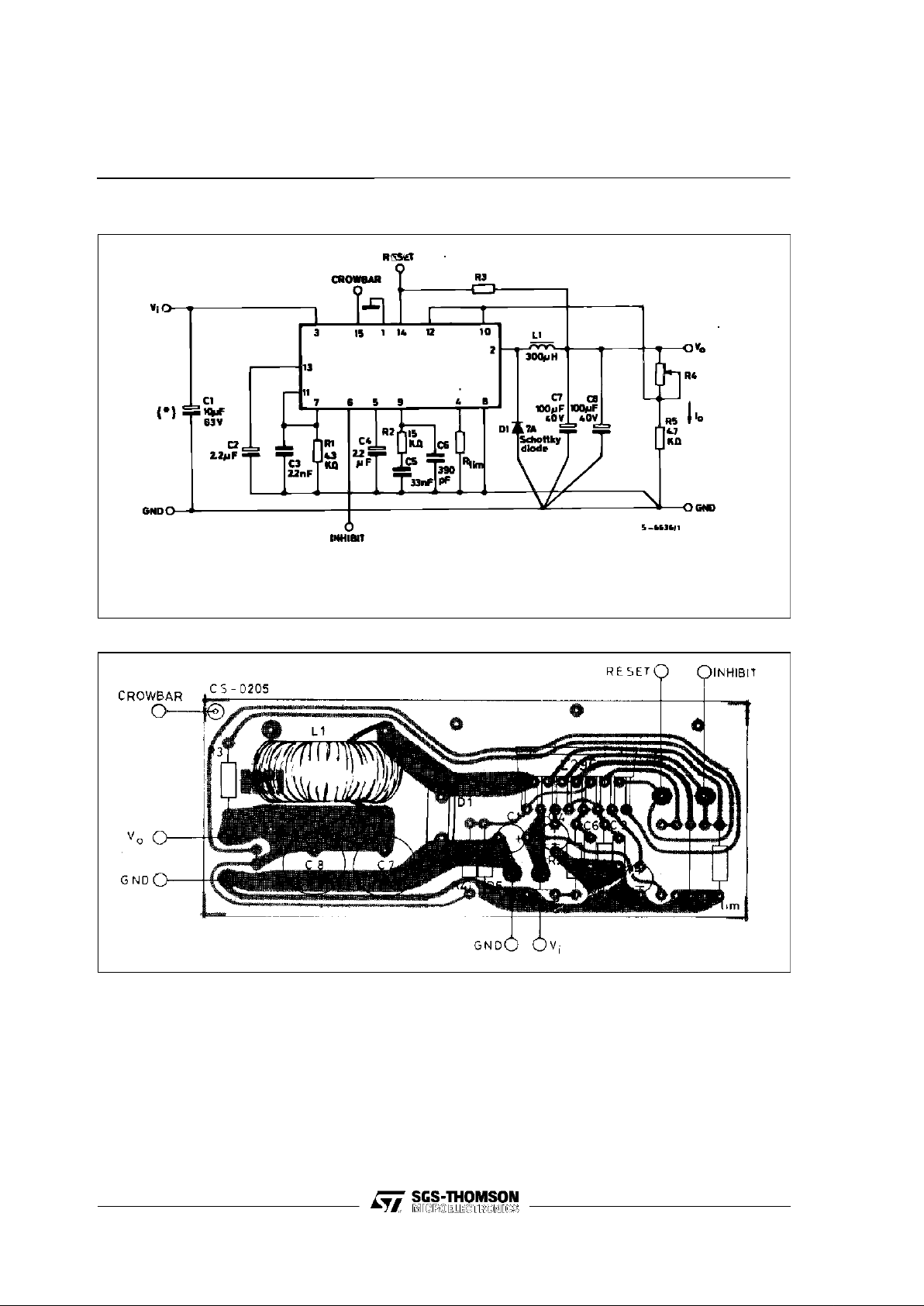
Figure 4 : DynamicTest Circuit
C7,C8 : EKR(ROE)
L1 :L = 300 µH at8 A Coretype : MAGNETICS 58930 - A2 MPP
N°turns : 43 Wire Gauge :1 mm (18 AWG) COGEMA 946044
(*) Minimumsuggested value(10 µF) to avoid oscillations.Ripple consideration leads to typicalvalueof 1000 µF or higher.
Figure 5 : PC.Board and Component Layoutof the Circuit of Figure 4 (1:1scale)
L296 - L296P
7/21
Page 8

Figure 6 : DCTestCircuits.
Figure 6a. Figure6b.
Figure 6c.
Figure 6d.
1 -Set V10FORV9=1V
2 -ChangeV
10
to obtain V9=3V
3-G
V
=
DV
9
=
2V
∆V
10
∆V
10
L296 - L296P
8/21
Page 9

Figure 7 : QuienscentDrainCurrent vs. Supply
Voltage(0 %DutyCycle - see fig.6a).
Figure8 : QuienscentDrain Current vs.Supply
Voltage(100 % Duty Cycleseefig. 6a).
Figure 9 : QuiescentDrain Currentvs. Junction
Temperature(0 % DutyCycle -
seefig. 6a).
Figure10 : QuiescentDrain Current vs.Junction
Temperature(100 % Duty Cycle see fig. 6a).
Figure 11 : ReferenceVoltage(pin 10) vs. V
I
(seefig. 4).
Figure12: ReferenceVoltage(pin10)vs.Junction
Temperature(see fig. 4).
L296 - L296P
9/21
Page 10

Figure 13 : Open LoopFrequencyand Phase
Responseof Error Amplifier
(seefig.6c).
Figure14 : SwitchingFrequencyvs. Input
Voltage(seefig.4).
Figure15 : SwitchingFrequency vs.Junction
Temperature(see fig. 4).
Figure 16 : SwitchingFrequencyvs. R1
(seefig.4).
Figure17 : LineTransientResponse(see fig. 4). Figure 18 : Load Transient Response(see fig.4).
L296 - L296P
10/21
Page 11

Figure 19 : Supply Voltage Ripple Rejectionvs.
Frequency(seefig.4).
Figure20 : DropoutVoltageBetweenPin3 and
Pin2 vs. Current at Pin2.
Figure 21 : DropoutVoltage BetweenPin 3 and
Pin2 vs. Junction Temperature.
Figure22 : Power DissipationDerating Curve.
Figure 23 : Power Dissipation(device only)vs.
Input Voltage.
Figure24 : Power Dissipation(device only)vs.
Inputvoltage.
L296 - L296P
11/21
Page 12

Figure 25 : Power Dissipation(device only)vs.
OutputVoltage(seefig. 4).
Figure26 : Power Dissipation(device only)vs.
OutputVoltage(see fig. 4).
Figure28 : Efficiencyvs.OutputCurrent.
Figure 29 : Efficiencyvs. OutputVoltage. Figure30 : Efficiencyvs.OutputVoltage.
Figure27: VoltageandCurrentWaveformsatPin2
(seefig. 4).
L296 - L296P
12/21
Page 13

Figure 31 : CurrentLimitingThresholdvs. R
pin 4
(L296Ponly).
Figure32 : Current LimitingThresholdvs.Junction
Temperature.
Figure 33 : CurrentLimitingThresholdvs.
SupplyVoltage.
L296 - L296P
13/21
Page 14

APPLICATION INFORMATION
Figure 34 : TypicalApplicationCircuit.
(*) Minimum value (10 µF) to avoidoscillations ; rippleconsideration leads to typicalvalue of1000µF orhigher L1 : 58930 - MPP COGEMA
946044 ; GUP 20 COGEMA 946045
SUGGESTEDINDUCTOR (L1)
Core Type No Turns Wire Gauge Air Gap
Magnetics 58930 – A2MPP 43 1.0 mm –
Thomson GUP 20 x 16 x 7 65 0.8 mm 1 mm
Siemens EC 35/17/10 (B6633& – G0500 – X127) 40 2 x 0.8 mm –
VOGT 250 µH Toroidal Coil, Part Number 5730501800
Resistor Values for Standard Output Voltages
V
0
R8 R7
12 V
15 V
18 V
24 V
4.7 KΩ
4.7 KΩ
4.7 KΩ
4.7 KΩ
6.2 KΩ
9.1 KΩ
12 KΩ
18 KΩ
L296 - L296P
14/21
Page 15

Figure 35 : P.C. Boardand Component Layoutof the Circuit of fig. 34 (1:1scale)
SELECTIONOF COMPONENT VALUES (see fig. 34)
Component
Recommended
Value
Purpose
Allowed Rage
Notes
Min. Max.
R1
R2
–
100 kΩ
Set Input Voltage
Threshold for Reset.
–
220kΩ
R1/R2
V
i min
5
− 1
If output voltage is sensed R1 and
R2 may be limited and pin 12
connected to pin 10.
R3 4.3 kΩ Sets Switching Frequency 1 kΩ 100kΩ
R4 10 kΩ Pull-down Resistor 22kΩ May be omitted and pin 6 grounded
if inhibit not used.
R5 15 kΩ Frequency Compensation 10kΩ
R6 Collector Load For Reset
Output
V
O
0.05A
Omitted if reset function not used.
R7
R8
–
4.7 kΩ
Divider to Set Output
Voltage
–
–
–
1kΩ
R7/R8 =
V
O
− V
REF
V
REF
-
R
iim
– Sets Current Limit Level 7.5kΩ If R
iim
is omitted and pin 4 left open
the current limit is internally fixed.
C1 10 µF Stability 2.2µF
C2 2.2 µF Sets Reset Delay – – Omitted if reset function not used.
C3 2.2 nF Sets Switching Frequency 1 nF 3.3nF
C4 2.2 µF Soft Start 1 µF – Also determines average short
circuit current.
C5 33 nF Frequency Compensation
C6 390 pF High Frequency
Compensation
– – Not required for 5 V operation.
C7, C8
L1
100 µF
300 µH
Output Filter –
100µH
–
Q1 Crowbar Protection The SCR must be able to withstand
the peak discharge current of the
output capacitor and the short
circuit current of the device.
D1 Recirculation Diode 7A Schottky or 35 ns t
rr
Diode.
L296 - L296P
15/21
Page 16

Figure 36 : A Minimal5.1V FixedRegulator.VeryFew Componentsare Required.
Figure 37 : 12 V/10 A Power Supply.
L296 - L296P
16/21
Page 17

Figure38 : ProgrammablePowerSupply.
Vo= 5.1 to 15 V
I
o
= 4 A max. (min.load current= 100mA)
ripple≤ 20mV
loadregulation (1A to 4 A) = 10 mV (V
o
=5.1V)
lineregulation (220V ± 15% and to I
o
= 3A)= 15 mV(Vo= 5.1 V)
Figure 39 : PreregulatorforDistributedSupplies.
(*)L2 and C2are necessary to reducethe switching frequency spikes.
L296 - L296P
17/21
Page 18

Figure 40 : In Multiple SuppliesSeveralL296s
canbe SynchronizedAs Shown.
Figure41 : VoltageSensingforRemoteLoad.
Figure 42 : A 5.1V/15 V/24 V Multiple Supply.Note the Synchronizationof the ThreeL296s.
L296 - L296P
18/21
Page 19

Figure 43 : 5.1V/2APower SupplyusingExternal
Limiting CurrentResistorandCrowbar ProtectionontheSupply Voltage
(L296Ponly)
SOFT-START AND REPETITIVEPOWER-ON
Whenthedeviceisrepetitivelypowered-on,thesoftstartcapacitor, C
SS
, must be dischargedrapidly to
ensurethateachstartis”soft”.Thiscanbeachieved
economicallyusingtheresetcircuit,asshowninFigure44.
In thiscircuit thedividerR1, R2connectedto pin 12
determines the minimum supply voltage, below
which theopencollectortransistoratthepin14output dischargesC
SS
.
Figure 44
Figure45
Figure46
Theapproximatedischargetimesobtainedwith this
circuit are :
CSS (µF) tDIS (µs)
2.2
4.7
10
200
300
600
Ifthesetimesarestilltoolong,anexternalPNPtran-
sistor may be added, as shownin Figure45 ; with
this circuit discharge times of a few microseconds
may be obtained.
HOW TO OBTAIN BOTH RESET AND
POWER FAIL
Figure46illustrateshowitispossibleto obtainatthe
same time both the power fail and reset functions
simply byaddingonediode(D) andoneresistor(R).
In this case the Reset delay time (pin 13) canonly
start whentheoutputvoltageis V
O
≥ V
REF
- 100mV
and thevoltageaccrossR2 is higherthan 4.5V.
Withthehysteresisresistoritispossibletofixthein-
put pin 12 hysteresisin order to increaseimmunity
to the 100Hzripple present onthe supplyvoltage.
Moreover,the power fail and reset delay time are
automaticallylockedtothesoft-start.Soft-startand
delayedreset are thustwo sequentialfunctions.
The hysteresis resistor should be In the range of
aboit 100kΩ andthe pull-up resistor of 1 to 2.2kΩ.
L296 - L296P
19/21
Page 20

PMMUL15V.EPS
MULTIWATT15 VERTICALPACKAGE MECHANICAL DATA
Dimensions
Millimeters Inches
Min. Typ. Max. Min. Typ. Max.
A 5 0.197
B 2.65 0.104
C 1.6 0.063
D 1 0.039
E 0.49 0.55 0.019 0.022
F 0.66 0.75 0.026 0.030
G 1.14 1.27 1.4 0.045 0.050 0.055
G1 17.57 17.78 17.91 0.692 0.700 0.705
H1 19.6 0.772
H2 20.2 0.795
L 22.1 22.6 0.870 0.890
L1 22 22.5 0.866 0.886
L2 17.65 18.1 0.695 0.713
L3 17.25 17.5 17.75 0.679 0.689 0.699
L4 10.3 10.7 10.9 0.406 0.421 0.429
L7 2.65 2.9 0.104 0.114
M 4.2 4.3 4.6 0.165 0.169 0.181
M1 4.5 5.08 5.3 0.177 0.200 0.209
S 1.9 2.6 0.075 0.102
S1 1.9 2.6 0.075 0.102
Dia. 1 3.65 3.85 0.144 0.152
MUL15V.TBL
L296 - L296P
20/21
Page 21

Information furnished is believed to be accurate and reliable. However, SGS-THOMSON Microelectronics assumes no responsibility for
the consequences of use of such information nor for any infringement of patents or other rights of third parties which may result from its
use. No license is granted by implication or otherwise under any patent or patent rights of SGS-THOMSON Microelectronics. Specifications mentioned in this publication are subject to change without notice. This publication supersedes and replaces all information previously supplied. SGS-THOMSON Microelectronics products are not authorized for use as critical components in life support devices or
systems without express written approval of SGS-THOMSON Microelectronics.
1994 SGS-THOMSON Microelectronics - All Rights Reserved
SGS-THOMSON Microelectronics GROUP OF COMPANIES
Australia - Brazil - France- Germany - Hong Kong - Italy - Japan - Korea - Malaysia - Malta - Morocco - The Netherlands - Singapore -
Spain - Sweden - Switzerland - Taiwan - Thaliand - UnitedKingdom - U.S.A.
L296 - L296P
21/21
 Loading...