


DUAL POWER OPERATIONAL AMPLIFIERS
.OUTPUTCURRENT TO1 A
.OPERATESAT LOW VOLTAGES
.SINGLEOR SPLITSUPPLY
.LARGE COMMON-MODE AND DIFFEREN-
TIALMODERANGE
.GROUNDCOMPATIBLEINPUTS
.LOWSATURATIONVOLTAGE
.THERMAL SHUTDOWN
DESCRIP TION
TheL272 isa monolithic integratedcircuits in Powerdip,Minidipand SO packagesintendedfor useas
poweroperationalamplifiers in a wide rangeof applicationsincludingservoamplifiersandpowersupplies,compacts disc, VCR, etc.
Thehighgainand high outputpower capabilityprovidesuperiorperformancewhateveranoperational
amplifier/powerboostercombinationisrequired.
L272
Powerdip
(8 +8)
Minidip
ORDERING NUMBERS : L272 (Powerdip)
SO16 (Narrow)
L272M (Minidip)
L272D (SO16 Narrow)
PIN CONNECTIONS (top view)
January 1995
L27 2M
L272D
1/10
L272
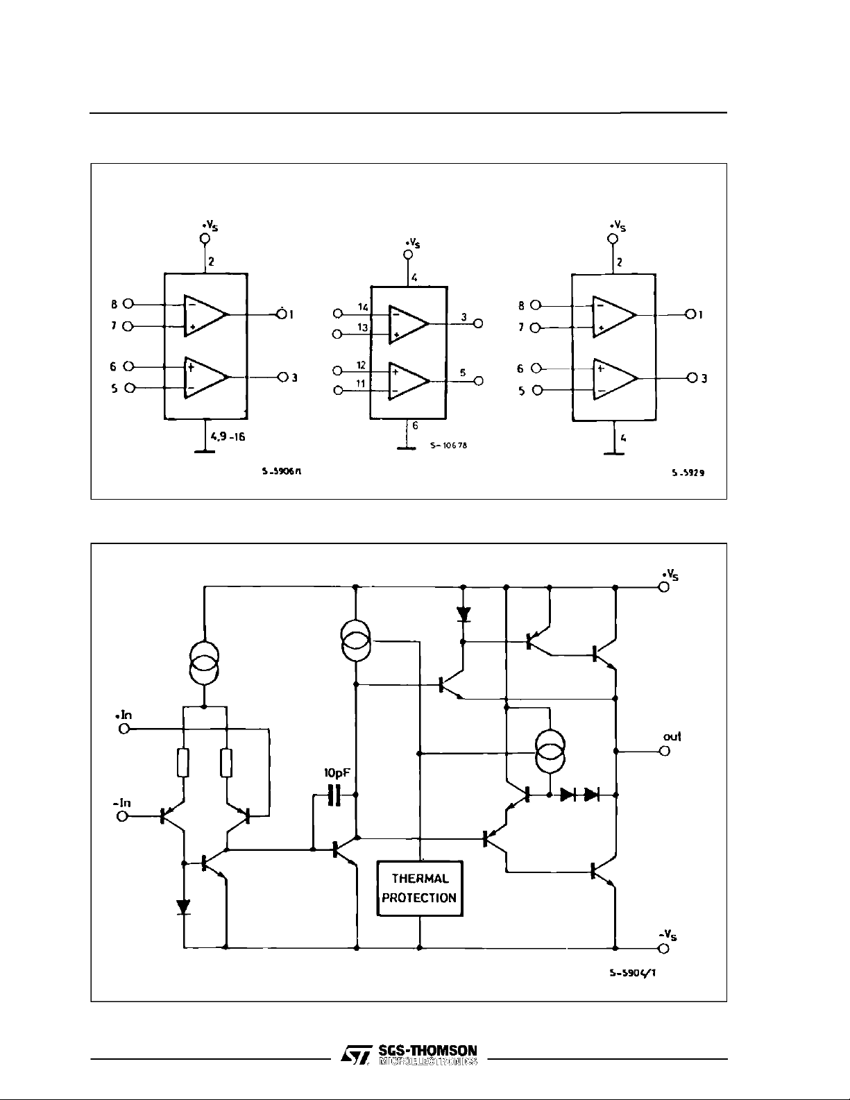
BLOCK DIAGRAMS
L272 L272ML272D
SCHEMATIC DIAGRAM (oneonly)
2/10
ABSOLUTE MAXIMUM RATINGS
Symbol Parameter Value Unit
V
V
V
I
o
I
p
P
tot
T
op
T
stg,Tj
s
Supply Voltage 28 V
Input Voltage V
i
Differential Input Voltage ± V
i
s
s
DC Output Current 1 A
Peak Output Current (non repetitive) 1.5 A
Power Dissipation at:
=80°C (L272), T
T
amb
=75°C (L272)
T
case
=50°C (L272M), T
amb
=90°C (L272D)
case
1.2
5
Operating Temperature Range (L272D) – 40 to 85 °C
Storage and Junction Temperature – 40 to 150 °C
THERMAL DATA
Symbol Parameter Powerdip SO16 Minidip Unit
R
th j-case
R
th j-amb
R
th j-alumina
* Thermal resistance junction-pin 4
** Thermal resistance junctions-pins with the chip soldered on the middle of an alumina supporting substrate measuring
15x 20mm; 0.65mm thickness and infinite heatsink.
Thermal Resistance Junction-pins Max. 15 – * 70
Thermal Resistance Junction-ambient Max. 70 – 100
Thermal Resistance Junction-alumina Max. – ** 50 –
L272
W
W
o
C/W
o
C/W
o
C/W
ELECTRICAL CHARACTERISTICS (VS= 24V, T
=25oC unless otherwise specified)
amb
Symbol Parameter Test Conditions Min. Typ. Max. Unit
V
s
I
s
I
b
V
os
I
os
Supply Voltage 4 28 V
Quiescent Drain Current VO=
S
V
= 24V
V
s
= 12V
s
2
8
7.51211mAmA
V
Input Bias Current 0.3 2.5 µA
Input Offset Voltage 15 60 mV
Input Offset Current 50 250 nA
SR Slew Rate 1V/µs
B Gain-bandwidth Product 350 kHz
R
G
v
e
N
I
N
Input Resistance 500 kΩ
i
O. L. Voltage Gain f = 100Hz
60 70
f = 1kHz
Input Noise Voltage B = 20kHz 10 µV
Input Noise Current B= 20kHz 200 pA
50
dB
dB
CRR Common Mode Rejection f = 1kHz 60 75 dB
SVR Supply Voltage Rejection f = 100Hz, R
= 24V
V
s
= ± 12V
V
s
= ± 6V
V
s
V
o
C
s
Output Voltage Swing Ip= 0.1A
= 0.5A 212322.5
I
p
Channel Separation f = 1 kHz; RL=10Ω,Gv= 30dB
= 24V
V
s
= ± 6V
V
s
d Distortion f = 1kHz, G
T
sd
Thermal Shutdown Junction
Temperature
= 10kΩ,VR= 0.5V
G
547062
56
60
60
= 3 dB, Vs= 24V, RL= ∞ 0.5 %
v
145 °C
dB
V
V
dB
3/10

L272
Figure 1 : QuiescentCurrent versus
SupplyVoltage
Figure2 : QuiescentDrain Current versus
Temperature
Figure 3 : OpenLoop VoltageGain Figure4 : OutputVoltageSwing versus
LoadCurrent
Figure 5 : OutputVoltageSwing versus
LoadCurrent
4/10
Figure6 : SupplyVoltageRejectionversus
Frequency

L272
Figure 7 : ChannelSeparationversus
Figure8 : Common Mode Rejection versus
Frequency
APPLICATION SUGGESTION
NOTE
In orderto avoid possible instabilityoccuringinto finalstagetheusualsuggestionsfor thelinearpower
stagesareuseful, as for instance :
- layoutaccuracy;
- a 100nFcapacitorcorrectedbetweensupplypins
and ground;
- boucherotcell(0.1 to0.2µF+1Ωseries)between
outputsand groundor acrossthe load.
Figure 9 : BidirectionalDC Motor Control with µPCompatible Inputs
Frequency
Figure 10 : Servocontrolfor Compact-disc
Figure 11 : CapstanMotorControlin VideoRecorders
5/10

L272
Figure 12 : Motor CurrentControlCircuit.
Note : The input voltage level is compatible with L291 (5-BIT D/A converter).
Figure 13 : BidirectionalSpeedControl of DCMotors.
2R3°R1
For circuitstabilityensurethat R
Thevoltageavailableat the terminalsof themotor isV
> where RM=internalresistanceofmotor.
X
R
M
=2(Vi⋅ )+Ro ⋅ ΙMwhereRo =
M
and IMisthe motorcurrent.
V
s
2R
2R°R1
X
6/10

POWERDIP 16 PACKAGE MECHANICAL DATA
L272
DIM.
MIN. TYP. MAX. MIN. TYP. MAX.
a1 0.51 0.020
B 0.85 1.40 0.033 0.055
b 0.50 0.020
b1 0.38 0.50 0.015 0.020
D 20.0 0.787
E 8.80 0.346
e 2.54 0.100
e3 17.78 0.700
F 7.10 0.280
I 5.10 0.201
L 3.30 0.130
Z 1.27 0.050
mm inch
7/10

L272
MINIDIP PACKAGE MECHANICAL DATA
DIM.
MIN. TYP. MAX. MIN. TYP. MAX.
A 3.32 0.131
a1 0.51 0.020
B 1.15 1.65 0.045 0.065
b 0.356 0.55 0.014 0.022
b1 0.204 0.304 0.008 0.012
D 10.92 0.430
E 7.95 9.75 0.313 0.384
e 2.54 0.100
e3 7.62 0.300
e4 7.62 0.300
F 6.6 0.260
I 5.08 0.200
L 3.18 3.81 0.125 0.150
Z 1.52 0.060
mm inch
8/10

SO16 NARROW PACKAGE MECHANICAL DATA
L272
DIM.
MIN. TYP. MAX. MIN. TYP. MAX.
A 1.75 0.069
a1 0.1 0.25 0.004 0.009
a2 1.6 0.063
b 0.35 0.46 0.014 0.018
b1 0.19 0.25 0.007 0.010
C 0.5 0.020
c1 45° (typ.)
D 9.8 10 0.386 0.394
E 5.8 6.2 0.228 0.244
e 1.27 0.050
e3 8.89 0.350
F 3.8 4.0 0.150 0.157
L 0.4 1.27 0.150 0.050
M 0.62 0.024
S8°(max.)
mm inch
9/10

L272
Information furnished is believed to be accurate and reliable. However, SGS-THOMSON Microelectronics assumes no responsibility for
the consequences of use of such information nor for any infringement of patents or other rights of third parties which may result from its
use. No license is granted by implication or otherwise under any patent or patent rights of SGS-THOMSON Microelectronics. Specifications mentioned in this publication are subject to change without notice. This publication supersedes and replaces all information previously supplied. SGS-THOMSON Microelectronics products are not authorized for use as critical components in life support devices or
systems without express written approval of SGS-THOMSON Microelectronics.
1995 SGS-THOMSON Microelectronics - All Rights Reserved
Australia - Brazil - France - Germany - Hong Kong - Italy - Japan - Korea - Malaysia - Malta - Morocco - The Netherlands - Singapore -
SGS-THOMSON Microelectronics GROUP OF COMPANIES
Spain - Sweden - Switzerland - Taiwan - Thaliand - United Kingdom - U.S.A.
10/10
 Loading...