

ADJUSTABLEVOLTAGE AND CURRENTREGULATOR
ADJUSTABLE OUTPUT CURRENT UP TO 2 A
(GUARANTEEDUP TOT
ADJUSTABLE OUTPUT VOLTAGE DOWN TO
2.85V
INPUT OVERVOLTAGE PROTECTION (UP TO
60 V, 10ms)
SHORTCIRCUIT PROTECTION
OUTPUT TRANSISTORS.O.A.PROTECTION
THERMAL OVERLOADPROTECTION
LOWBIAS CURRENT ON REGULATIONPIN
LOWSTANDBYCURRENT DRAIN
DESCRIPTION
The L200 is a monolithic integratedcircuit for voltage and current programmable regulation. It is
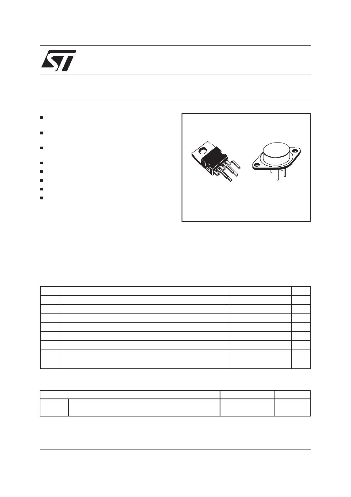
available in Pentawatt
metalcase.Currentlimiting,powerlimiting,thermal
shutdown and input overvoltage protection (up to
= 150°C)
j
package or 4-lead TO-3
L200
Pentawatt
60 V) make the L200 virtually blow-outproof.
The L200 can be used to replace fixed voltage
regulators when high output voltage precision is
required and eliminates the need to stock a range
of fixed voltageregulators.
TO-3(4 lead)
ABSOLUTE MAXIMUM RATINGS
Symbol Parameter Value Unit
V
DC Input Voltage 40 V
i
V
PeakInput Voltage(10 ms) 60 V
i
DropoutVoltage 32 V
V
∆
i-o
I
Output Current internally limited
o
P
PowerDissipation internally limited
tot
Storage Temperature -55 to 150
T
stg
Operating Junction Temperaturefor L200C -25 to 150
T
op
forL200 -55 to 150 °
THERMALDATA
TO-3 Pentawatt
R
th j-case
R
thj-amb
January 2000
Thermal Resistance Junction-case Max
Thermal Resistance Junction-ambient Max
4 °C/W 3 °C/W
35 °C/W 50 °C/W
C
°
C
°
C
1/12
L200
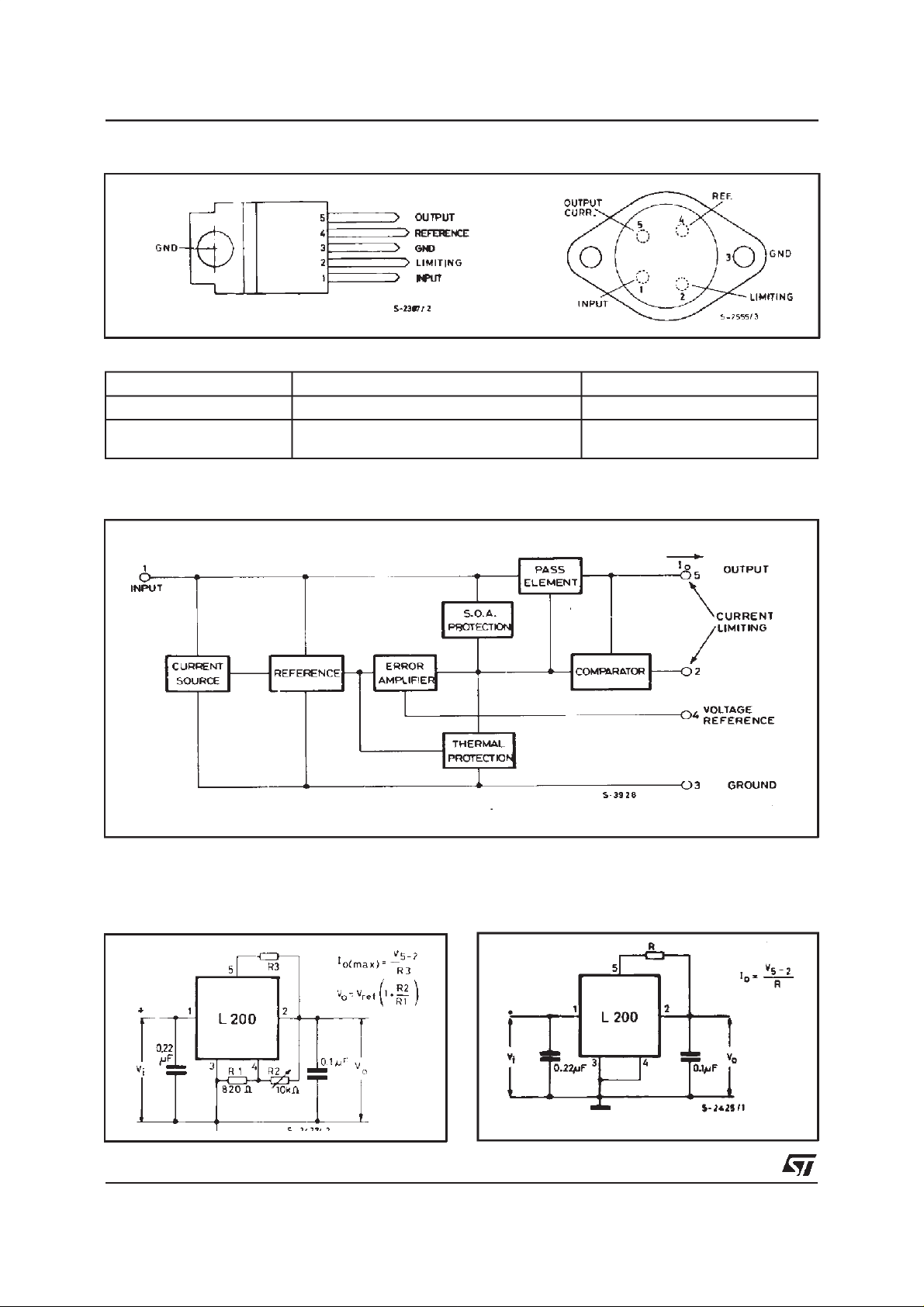
CONNECTION DIAGRAMS AND ORDER CODES
Type Pentawatt
L200 L200 T
L200 C L200 CH
L200 CV
BLOCK DIAGRAM
(top views)
TO-3
L200 CT
APPLICATION CIRCUITS
Figure 1. Programmable Voltage Regulator
with CurrentLimiting
2/12
Figure 2.ProgrammableCurrent Regulator.
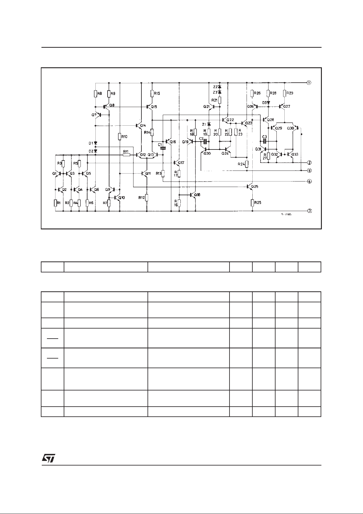
SCHEMATIC DIAGRAM
L200
ELECTRICAL CHARACTERISTICS
(T
amb
C, unlessotherwise specified)
=25
°
Symbol Parameter TestConditions Min. Typ. Max. Unit
VOLTAGE REGULATIONLOOP
I
Quiescent drain Current (pin 3) Vi= 20 V 4.2 9.2 mA
d
e
Output Noise Voltage Vo= Vref Io=10mA
N
Output Voltage Range Io= 10 mA 2.85 36 V
V
o
V
∆
o
VoltageLoad Regulation
(note 1)
V
o
V
∆
i
Line Regulation V0=5V
∆ V
o
SVR Supply VoltageRejection
Droupout Voltagebetween Pins 1
V
∆
i-o
and 5
V
Reference Voltage(pin 4) Vi=20V Io= 10 mA 2.64 2.77 2.86 V
ref
B = 1 MHz 80
I
=2A
∆
o
I
= 1.5 A
∆
o
V
= 8 to 18 V 48 60 dB
i
V
=5V Io= 500 mA
0
∆V
=10V
i
f = 100 Hz (note 2)
pp
I
= 1.5 A
o
∆
V
2%
≤
0
48 60 dB
0.15
0.1
1
0.9
2 2.5 V
V
µ
%
%
3/12

L200
ELECTRICALCHARACTERISTICS
(continued)
Symbol Parameter TestConditions Min. Typ. Max. Unit
= 20 V Io = 10mA
V
∆
I
4
∆ I
T
∆
Z
o
AverageTemperature Coefficient
ref
of ReferenceVoltage
Bias Current and Pin 4 3 10
AverageTemperature
4
Coefficient (pin 4)
• I
4
Output Impedance Vi=10V Vo=V
V
i
for Tj = - 25 to 125°C
for Tj =125 to 150°C
-0.25
-1.5
-0.5
ref
Io= 0.5 A f = 100 Hz 1.5
CURRENT REGULATIONLOOP
V
SC
V
∆
T
∆
•
I
∆
I
o
Current Limit Sense Voltage
between Pins 5 and 2
SC
AverageTemperature
Coefficient of V
V
SC
o
Current LoadRegulation
SC
Vi=10V Vo=V
ref
I5= 100 mA 0.38 0.45 0.52 V
0.03 %/°
Vi = 10 V ∆Vo = 3V
= 0.5 A
I
o
I
=1A
o
I
= 1.5 A
o
1.4
1
0.9
mV/°C
mV/°C
A
µ
%/°C
mΩ
C
%
%
%
I
SC
PeakShort Circuit Current Vi-V0=14V
(pins 2 and 5 short circuited) 3.6 A
Note 1: A load step of 2 A can be applied provited that input-output differentialvoltage is lower than 20V (see Figure3).
Note 2: The same performance can be maintained at higher output levelsif a bypassing capacitor is provited between pins 2 and 4.
Figure 3. Typical Safe Operating Area
Protection.
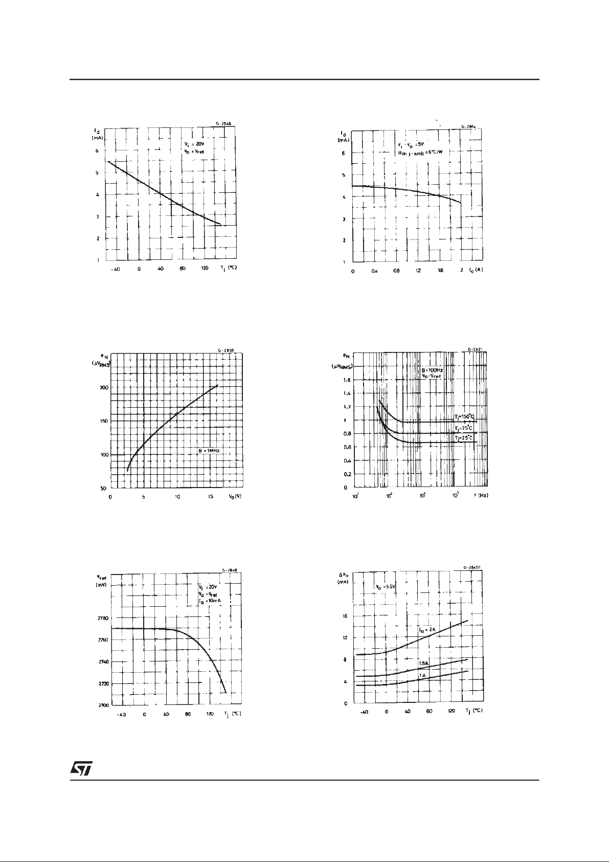
Figure 4. Quiescent Current vs. Supply
Voltage.
4/12
L200
Figure 5. Quiescent Current vs. Junction
Voltage.
Figure7. OutputNoise Voltage vs. Output
Voltage.
Figure 6. Quiescent Current vs. Output
Current.
Fi gu re 8. Out p ut Noi se Volt a g e vs.
Frequency.
Figure 9. Reference Voltage vs. Junction
Temperature.
Figure 10. Voltage Load Regulation vs.
JunctionTemperature.
5/12
L200
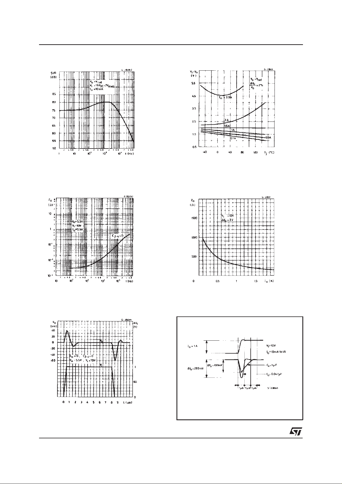
Figure 11. Supply Voltage Rejection vs.
Frequency.
Figure 13. Output I mpedance v s.
Frequency.
Figure 12. Dropout Voltage vs. Junction
Temperature.
Figure 14. Output Impedance vs. Output
Current.
Figure15. VoltageTransientReponse. Figure 16. Load TransientReponse.
6/12
L200
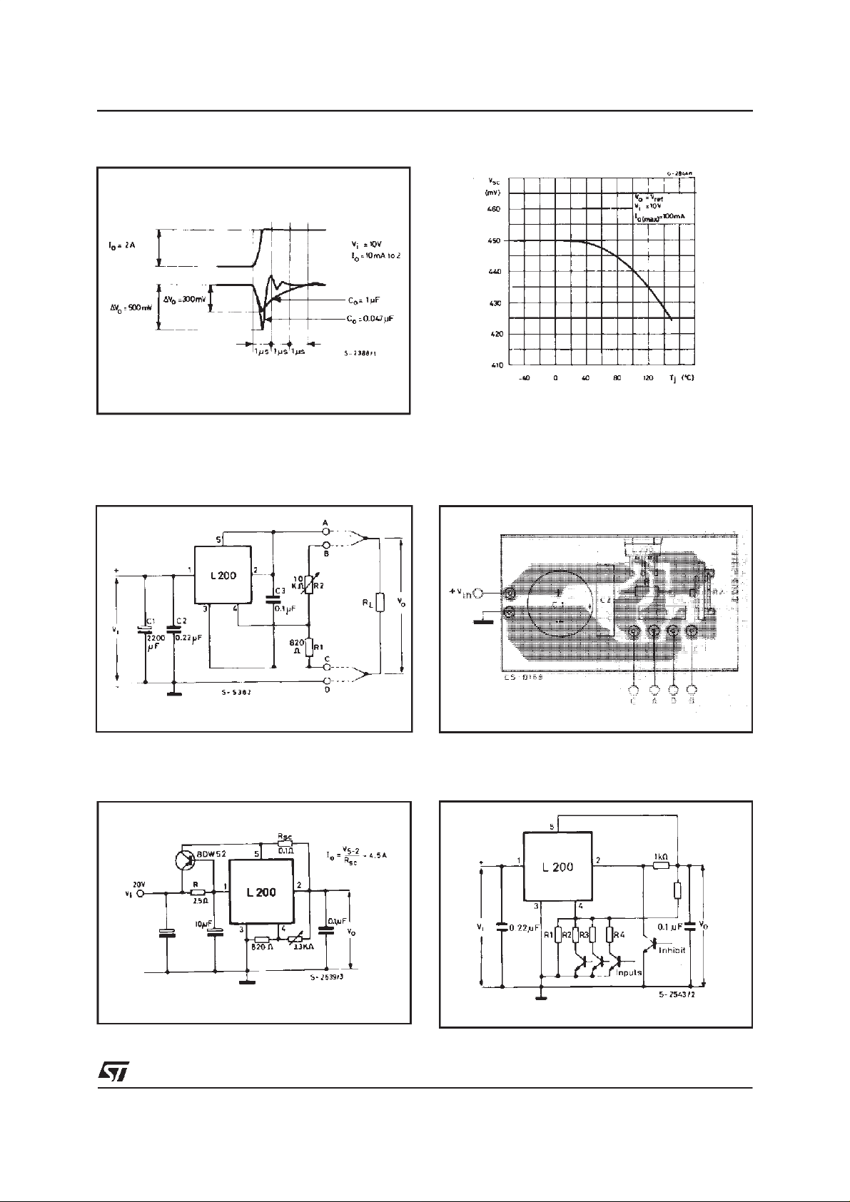
Figure17.Load Transient Reponse
APPLICATIONS CIRCUITS
Figure19. - ProgrammableVoltageRegulator
Figure 18. Current Limit Sense Voltage vs.
JunctionTemperature.
Figure20.- P.C.Board and ComponentsLayout
of Figure 19.
Figure21.- HighCurrentVoltageRegulatorwith
Short CircuitProtection.
Figure 22. - Digitally Selected Regulator with
Inhibit.
7/12
L200
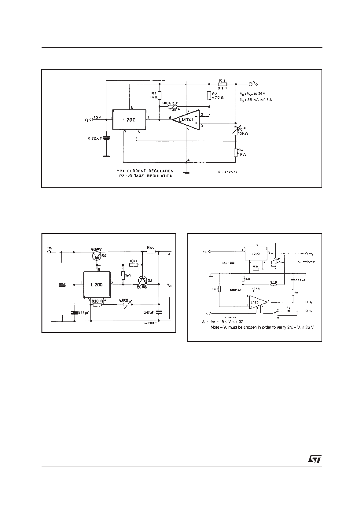
Figure23. ProgrammableVoltageand CurrentRegulator.
Note: Connecting point A to a negative voltage (for example - 3V/10 mA) it is possibleto extend the output voltage
range down to 0 V and obtainthe current limiting down to this level(output short-circuit condition).
Figure 24. High Current Regulator with NPN
PassTransistor.
Figure25.High Current TrackingRegualtor.
8/12

L200
Figure26. High Input and Output Voltage.
Figure28. 30 W Motor Speed Control.
Figure27. ConstantCurrent Battery Charger.
The resistors R1and R2determine the final charging voltage and R
charge ofthe battery throught the regulator.
The resistor RL limits the reverse currents through ther
regulator (which should be 100 mA max) when the battery is accidentally reverse connected. If R
with a bulb of 12 V/50 mA rating this will indicate incorrect connection.
the initial charging current. D1prevents dis-
SC
is in series
L
Figure29.LowwTurnon.
Figure30. Light Controller.
9/12

L200
DIM.
MIN. TYP. MAX. MIN. TYP. MAX.
mm inch
A 4.8 0.189
C 1.37 0.054
D 2.4 2.8 0.094 0.110
D1 1.2 1.35 0.047 0.053
E 0.35 0.55 0.014 0.022
E1 0.76 1.19 0.030 0.047
F 0.8 1.05 0.031 0.041
F1 1 1.4 0.039 0.055
G 3.2 3.4 3.6 0.126 0.134 0.142
G1 6.6 6.8 7 0.260 0.268 0.276
H2 10.4 0.409
H3 10.05 10.4 0.396 0.409
L 17.55 17.85 18.15 0.691 0.703 0.715
L1 15.55 15.75 15.95 0.612 0.620 0.628
L2 21.2 21.4 21.6 0.831 0.843 0.850
L3 22.3 22.5 22.7 0.878 0.886 0.894
L4 1.29 0.051
L5 2.6 3 0.102 0.118
L6 15.1 15.8 0.594
0.622
L7 6 6.6 0.236 0.260
L9 0.2 0.008
M 4.23 4.5 4.75 0.167 0.177 0.187
M1 3.75 4 4.25 0.148 0.157 0.167
V4 40°(typ.)
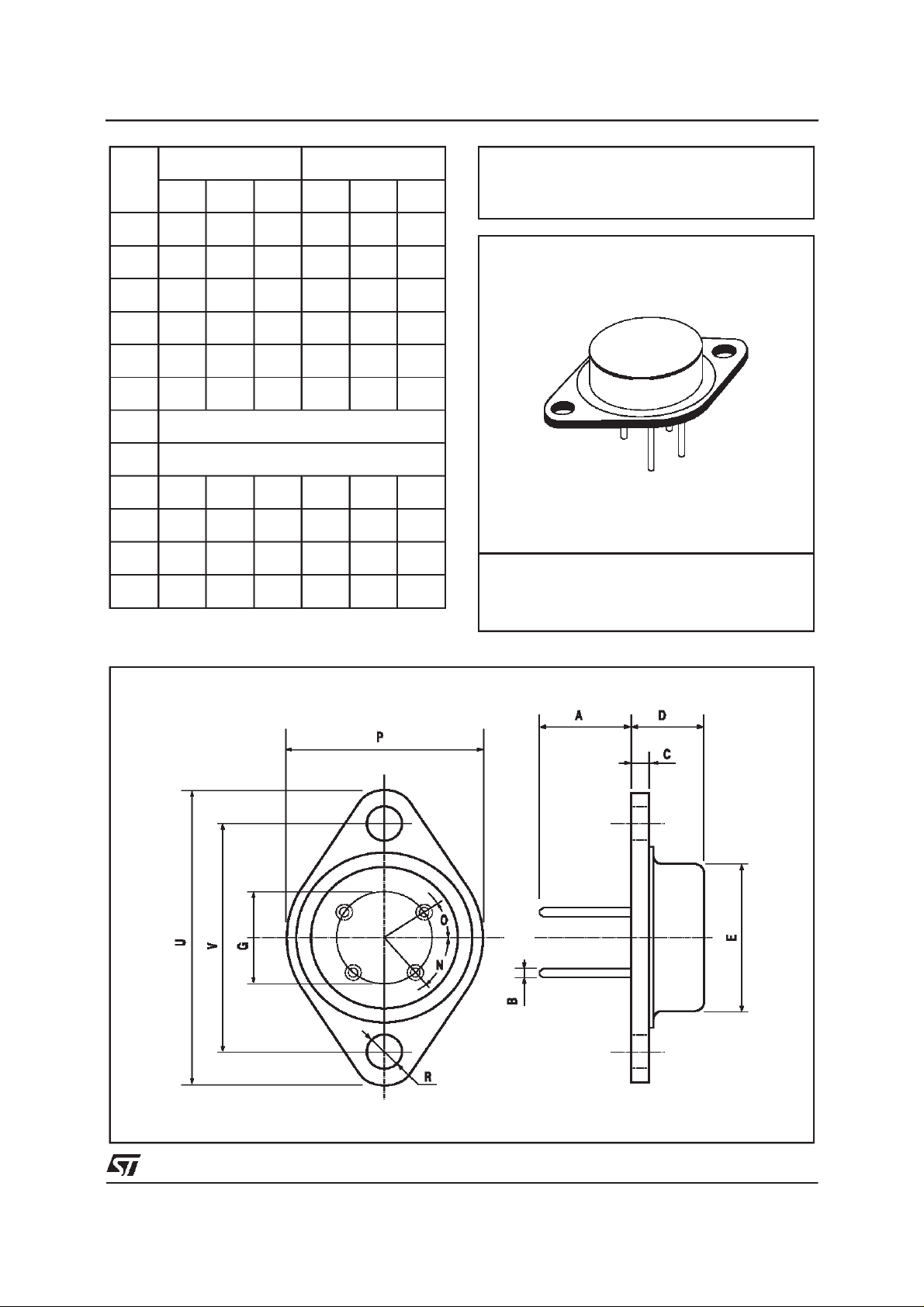
OUTLINE AND
MECHANICAL DATA
Pentawatt V
A
H3
B
H1
L
L1
L8
VV
C
L5
Dia.
L7
L6
D1
V1
R
D
L2
L3
RESIN BETWEEN
V3
R
R
V4
F1
LEADS
H2
E
M1
M
V4
GG1
F
L9
VV
H2
F
E1
E
V4
10/12
L200
DIM.
MIN. TYP. MAX. MIN. TYP. MAX.
A 11.8 0.46
B (*) 1 0.39
C 2.5 0.098
D 9.6 0.37
E 20 0.78
G 12.7 0.50
N50° (typ.)
O30° (typ.)
P 26.2 1.03
R 3.88 4.20 0.15 0.16
U 39.5 1.55
V 30.1 1.18
mm inch
OUTLINE AND
MECHANICAL DATA
TO3 4-Leads
(*) Measured withGauge
11/12

L200
Informationfurnished is believedto be accurateand reliable.However,STMicroelectronics assumes no responsibility for the consequences of
use of such information nor for any infringement of patents or other rights of third parties which may result from its use.No license is granted
by implication or otherwise under any patent or patent rights of STMicroelectronics. Specification mentioned in this publicationare subjectto
change without notice. This publication supersedes and replaces all information previously supplied. STMicroelectronics products are not
authorized for use as critical components in lifesupport devicesor systems withoutexpress written approval of STMicroelectronics.
The ST logois a registered trademark of STMicroelectronics
2000 STMicroelectronics – Printed in Italy – All Rights Reserved
STMicroelectronics GROUP OF COMPANIES
Australia- Brazil- China - Finland - France - Germany - Hong Kong - India- Italy- Japan - Malaysia - Malta - Morocco -
Singapore- Spain - Sweden - Switzerland - UnitedKingdom - U.S.A.
http://www.st.com
12/12
 Loading...