

Datasheet KD1083D2T30, KD1083D2T25, KD1083D2T, KD1083V33, KD1083V30 Datasheet (SGS Thomson Microelectronics)
...
7.5A LOW DROP POSITIVE VOLTAGE REGULATOR
■ THREE TERMINAL ADJUSTABLE OR FIXED
OUTPUT VOLTAGE 1.5V,1.8V, 2.5V, 3.0, 3.3V
■ OUTPUT CURRENT UP TO 7.5A
■ 1.4V MAX DROPOUT V OLTAGE AT FULL
LOAD
■ LINE REGULATION: MAX 0.2% OVE R FULL
TEMPERATURE RANGE
■ LOAD REGULATION: MAX 0.5% OVER FULL
TEMPERATURE RANGE
■ OUTPUT CURRENT LIMIT
■ THERMAL SHUTDOWN PROTECTION
WITH HYSTERESIS
■ WIDE OPE RATING TEMPERATURE RANGE
-40°C TO 125°C
■ PINOUT COM PATIBILITY WITH STANDARD
ADJUSTABLE VREG
DESCRIPTION
The KD1083 is a low drop linear voltage regula tor,
proposed both in adjustable and fixed version and
designed for use in applications requiring output
currents up to 7.5A. Dropout v oltage is
guaranteed not to exceed 1.4V at maximum
output current while it decreases at
lighter loads. The KD10 83 also features an
on-chip output current limit function and a thermal
shutdown pro tection with hysteresis, preventing
from excessive p ower dissipation in case of
SCHEMATIC DIAGRAM
KD1083
ADJUSTABLE AND FIXED
PRELIMINARY DATA
TO-220 D2PAK
insufficient heatsinking. The KD1083 is fully pin to
pin compatible with the older 3-terminal adjustable
regulators, but it has better performances in terms
of drop and output voltage precis ion.
On chip trimming allows the regulator to reach a
very t ight output voltage tolerance, within ±2% at
25°C and 2% over the full temperature range.
Unlike v oltage regulators using a PNP transistor
as series pass element in which a considerable
fraction of the output current is wasted as
quiescent current, the LD1083 quiescent current
flows almost entirely into the load, improving the
efficiency.
Only a 10µF minimum capacitor is required for
output stability.
1/11October 2002
This is preliminary information on a new product now in development or undergoing evaluation. Details are subject to change without notice.

KD1083
ABSOLUTE MAXIMUM RATINGS
Symbol Parameter Value Unit
V
I
P
T
T
Absolute Maximum Ratings are those values beyond which damage to the device may occur. Functional operation under these condition is
not implied.
THERMAL DATA
DC Input to Output Voltage
IN
Output Current
O
Power Dissipation
D
Storage Temperature Range
stg
Operating Junction Temperature Range
op
from -0.3 to 10 V
Internally Limited A
Internally Limited W
-55 to +150 °C
-40 to +125 °C
Symbol Parameter TO-220
R
thj-case
R
thj-amb
Thermal Resistance Junction-case
Thermal Resistance Junction-ambient
3 3 °C/W
50 62.5 °C/W
CONNECTION DIAGRAM (top view)
TO-220 D2PAK
ORDERING CODES
TO-220
KD1083V15 KD1083D2T15 1.5V
KD1083V18 KD1083D2T18 1.8V
KD1083V25 KD1083D2T25 2.5V
KD1083V30 KD1083D2T30 3.0V
KD1083V33 KD1083D2T33 3.3V
KD1083V KD1083D2T Adjustable
(*) Available in Tape & Reel with the suffix "R" for fixed version and "-R" for adjustable version.
2
D
PAK(*)
2
D
PAK
OUTPUT VOLTAGE
Unit
TYPICAL APPLICATION CIRCUITS
2/11
VO=V
REF
R
2
(1 + )
R
1

KD1083
ELECTRICAL CHARACTERISTICS OF KD1083 (VIN=3V, CI=CO=10µF, Tj= -40 to 125°C, unless
otherwise s pec ified .)
Symbol Parameter Test Conditions Min. Typ. Max. Unit
V
∆V
∆V
I
O(min)
∆I
SVR Supply Voltage Rejection f = 120 Hz, C
T
T
NOTE 1: See short-circuit current curve for available output current at fixed dropout.
Reference Voltage IO=10mA , (VIN-VO)=3V,Tj= 25°C 1.237 1.25 1.262 V
REF
= 0.01 to 7.5A, (VIN-VO) = 1.5 to 5.75V
I
O
1.225 1.25 1.275 V
(note1)
Line Regulation IO=10mA, (VIN-VO) = 1.5 to 5.75V 0.015 0.2 %
REF
Load Regulation (VIN-VO)=3V, IO = 10mA to 7.5A 0.3 0.5 %
REF
V
Dropout Voltage ∆VO=2%, IO=7.5A 1.05 1.4 V
d
Short Circuit Current (VIN-VO) = 1.5 to 5.75V 8.5 A
I
sc
Minimum Load Current (VIN-VO) = 1.5 to 5.75V 5 10 mA
Adjust Pin Current IO = 10mA to 7.5A 40 80 µA
I
ADJ
Adjust Pin Current Change IO = 10mA to 7.5A, (VIN-VO) = 1.5 to 5.75V 0.2 5 µA
ADJ
60 75 dB
0.003 %
175 °C
5°C
eN RMS Output Noise Voltage
(% of V
Thermal Shutdown
SHDN
Threshold
Thermal Shutdown
HYST
Hysteresis
)
O
=25µF, IO= 7.5A,
O
)=3V, VPP=1V
(V
IN-VO
T
= 25°C, f =10Hz to 10kHz, IO=10mA,
A
)=3V
(V
IN-VO
ELECTRICAL CHARACTERISTICS OF KD1083#15 (VIN=3.25V, CI=CO=10µF, Tj= -40 to 125°C,
unless otherwise specified.)
Symbol Parameter Test Conditions Min. Typ. Max. Unit
Output Voltage IO=10mA , (VIN-VO)=3V, Tj= 25°C 1.485 1.5 1.515 V
V
O
= 0 to 7.5A, (VIN-VO) = 1.5 to 5.5V
I
O
(note1)
Line Regulation IO=10mA, (VIN-VO) = 1.5 to 5.5V 0.015 0.2 %
∆V
O
Load Regulation (VIN-VO)=3V, IO = 0 to 7.5A 0.3 0.5 %
∆V
O
Dropout Voltage ∆VO=2%, IO=7.5A 1.05 1.4 V
V
d
I
Short Circuit Current (VIN-VO) = 1.5 to 5.5V 8.5 A
sc
Quiescent Current (VIN-VO) = 1.5 to 5.5V, IO=0A 5 10 mA
I
d
SVR Supply Voltage Rejection f = 120 Hz, C
(V
IN-VO
T
eN RMS Output Noise Voltage
(% of V
T
T
NOTE 1: See short-circuit current curve for available output current at fixed dropout.
Thermal Shutdown
SHDN
Threshold
Thermal Shutdown
HYST
Hysteresis
)
O
= 25°C, f =10Hz to 10kHz, IO=10mA,
A
(V
IN-VO
=25µF, IO= 7.5A,
O
)=3V,VPP=1V
)=3V
1.47 1.5 1.53 V
58.6 73.4 dB
0.003 %
175 °C
5°C
3/11
KD1083
ELECTRICAL CHARACTERISTICS OF KD1083#18(VIN=3.5V, CI=CO=10µF, Tj= -40 to 125°C, unless
otherwise s pec ified .)
Symbol Parameter Test Conditions Min. Typ. Max. Unit
V
Output Voltage IO=10mA , (VIN-VO)=3V, Tj= 25°C 1.782 1.8 1.818 V
O
= 0 to 7.5A, (VIN-VO) = 1.5 to 5.2V
I
O
(note1)
Line Regulation IO=10mA, (VIN-VO) = 1.5 to 5.2V 0.015 0.2 %
∆V
O
Load Regulation (VIN-VO)=3V, IO = 0 to 7.5A 0.3 0.5 %
∆V
O
V
Dropout Voltage ∆VO=2%, IO=7.5A 1.05 1.4 V
d
Short Circuit Current (VIN-VO) = 1.5 to 5.2V 8.5 A
I
sc
Quiescent Current (VIN-VO) = 1.5 to 5.2V, IO=0A 5 10 mA
I
d
SVR Supply Voltage Rejection f = 120 Hz, C
(V
IN-VO
T
eN RMS Output Noise Voltage
(% of V
T
T
NOTE 1: See short-circuit current curve for available output current at fixed dropout.
Thermal Shutdown
SHDN
Threshold
Thermal Shutdown
HYST
Hysteresis
)
O
= 25°C, f =10Hz to 10kHz, IO=10mA,
A
(V
IN-VO
=25µF, IO= 7.5A,
O
)=3V,VPP=1V
)=3V
1.764 1.8 1.836 V
57 71.8 dB
0.003 %
175 °C
5°C
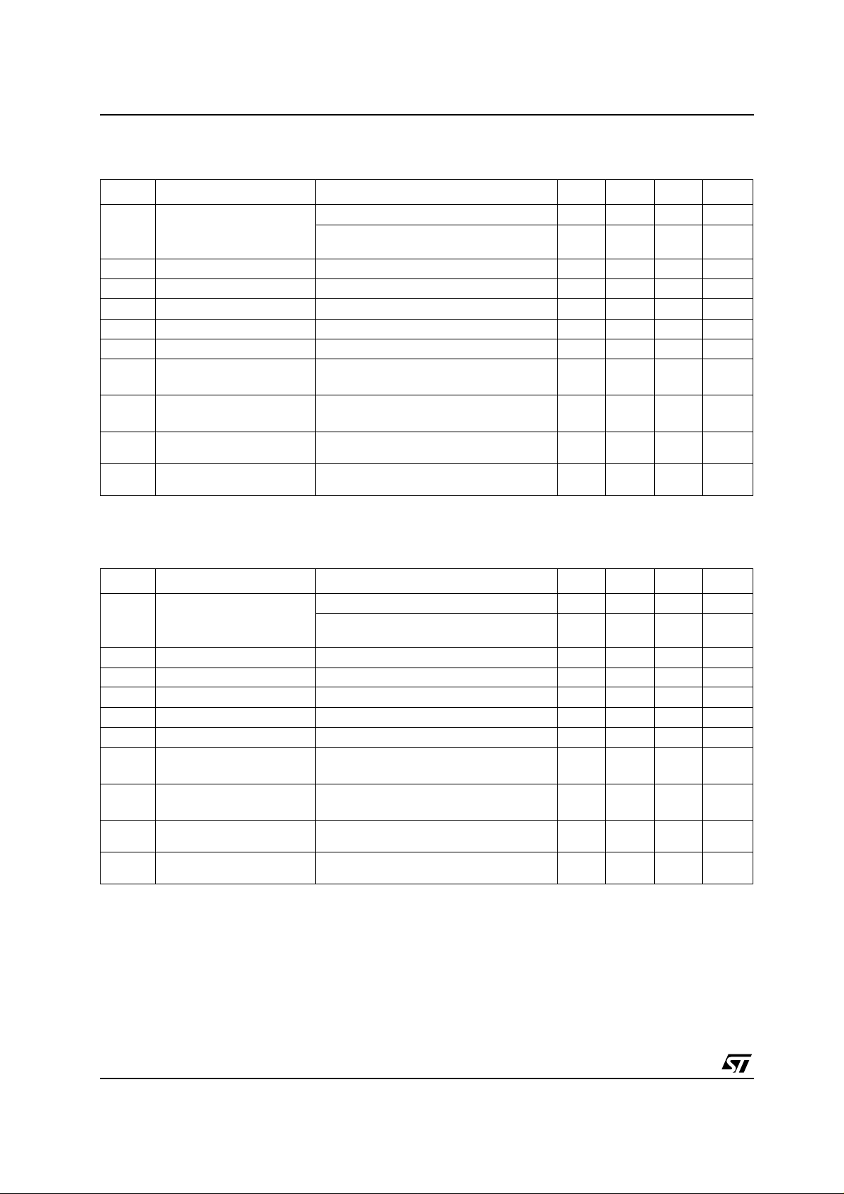
ELECTRICAL CHARACTERISTICS OF KD1083#25 (VIN=4.25V, CI=CO=10µF, Tj= -40 to 125°C,
unless otherwise specified.)
Symbol Parameter Test Conditions Min. Typ. Max. Unit
Output Voltage IO=10mA , (VIN-VO)=3V, Tj= 25°C 2.475 2.5 2.525 V
V
O
= 0 to 7.5A, (VIN-VO) = 1.5 to 4.5V
I
O
(note 1)
Line Regulation IO=10mA, (VIN-VO) = 1.5 to 4.5V 0.015 0.2 %
∆V
O
Load Regulation (VIN-VO)=3V, IO = 0 to 7.5A 0.3 0.5 %
∆V
O
Dropout Voltage ∆VO=2%, IO=7.5A 1.05 1.4 V
V
d
I
Short Circuit Current (VIN-VO) = 1.5 to 4.5V 8.5 A
sc
Quiescent Current (VIN-VO) = 1.5 to 4.5V, IO=0A 5 10 mA
I
d
SVR Supply Voltage Rejection f = 120 Hz, C
(V
IN-VO
T
eN RMS Output Noise Voltage
(% of V
T
T
NOTE 1: See short-circuit current curve for available output current at fixed dropout.
Thermal Shutdown
SHDN
Threshold
Thermal Shutdown
HYST
Hysteresis
)
O
= 25°C, f =10Hz to 10kHz, IO=10mA,
A
(V
IN-VO
=25µF, IO= 7.5A,
O
)=3V,VPP=1V
)=3V
2.45 2.5 2.55 V
54.1 68.9 dB
0.003 %
175 °C
5°C
4/11

KD1083
ELECTRICAL CHARACTERISTICS OF KD1083#30 (VIN=4.75V, CI=CO=10µF, Tj= -40 to 125°C,
unless otherwise specified.)
Symbol Parameter Test Conditions Min. Typ. Max. Unit
V
Output Voltage IO=10mA , (VIN-VO)=3V, Tj= 25°C 2.97 3.0 3.03 V
O
= 0 to 7.5A, (VIN-VO) =1.5to4V
I
O
(note 1)
∆V
∆V
SVR Supply Voltage Rejection f = 120 Hz, C
T
T
NOTE 1: See short-circuit current curve for available output current at fixed dropout.
Line Regulation IO=10mA, (VIN-VO) = 1.5 to 4V 0.015 0.2 %
O
Load Regulation (VIN-VO)=3V,IO = 0 to 7.5A 0.3 0.5 %
O
V
Dropout Voltage ∆VO=2%, IO=7.5A 1.05 1.4 V
d
Short Circuit Current (VIN-VO) = 1.5 to 4V 8.5 A
I
sc
Quiescent Current (VIN-VO) = 1.5 to 4V, IO=0A 5 10 mA
I
d
=25µF, IO= 7.5A,
O
)=3V,VPP=1V
)=3V
eN RMS Output Noise Voltage
(% of V
Thermal Shutdown
SHDN
Threshold
Thermal Shutdown
HYST
Hysteresis
)
O
(V
IN-VO
T
= 25°C, f =10Hz to 10kHz, IO=10mA,
A
(V
IN-VO
2.94 3 3.06 V
52.5 67.3 dB
0.003 %
175 °C
5°C
ELECTRICAL CHARACTERISTICS OF KD1083#33 (VIN=5.0V, CI=CO=10µF,Tj= -40to 125°C,unless
otherwise specified.)
Symbol Parameter Test Conditions Min. Typ. Max. Unit
Output Voltage IO=10mA , (VIN-VO)=3V, Tj= 25°C 3.267 3.3 3.333 V
V
O
= 0 to 7.5A, (VIN-VO) = 1.5 to 3.7V
I
O
(note 1)
∆V
∆V
SVR Supply Voltage Rejection f = 120 Hz, C
T
T
NOTE 1: See short-circuit current curve for available output current at fixed dropout.
Line Regulation IO=10mA, (VIN-VO) = 1.5 to 3.7V 0.015 0.2 %
O
Load Regulation (VIN-VO)=3V,IO = 0 to 7.5A 0.3 0.5 %
O
Dropout Voltage ∆VO=2%, IO=7.5A 1.05 1.4 V
V
d
I
Short Circuit Current (VIN-VO) = 1.5 to 3.7V 8.5 A
sc
Quiescent Current (VIN-VO) = 1.5 to 3.7V, IO=0A 5 10 mA
I
d
=25µF, IO= 7.5A,
O
)=3V,VPP=1V
)=3V
eN RMS Output Noise Voltage
(% of V
Thermal Shutdown
SHDN
Threshold
Thermal Shutdown
HYST
Hysteresis
)
O
(V
IN-VO
T
= 25°C, f =10Hz to 10kHz, IO=10mA,
A
(V
IN-VO
3.234 3.3 3.366 V
51.7 66.5 dB
0.003 %
175 °C
5°C
5/11

KD1083
TYPICAL CHARACTERISTICS
Figure1 : Referen ce Voltage vs Temperature
Figure2 : Referen ce Voltage vs Temperature
(CI=CO=10µF(tantalum), unless otherwise specified)
Figure4 : Line Regulation vs Temperature
Figure5 : Load Regulation vs Temperature
Figure3 : Referen ce Voltage vs Temperature
6/11
Figure6 : D ro pout Voltage v s T emperature

KD1083
Figure7 : Dropout Voltage vs Temperature
Figure8 : Adj ust Pin Current vs Temperature
Figure10 : Minimum Load Current vs
Temperature
Figure11 : Dropout Voltage vs Output Current
Figure9 : Quiescent Current vs Temperature
Figure12 : Supply Voltage Rejection vs Output
Current
7/11

KD1083
V
13V,I
100mA,C
C
V
12V,I
100mA,C
C
V
12 V,I
C
C
V
12 V,I
C
C
Figure13 : Short Circuit Current vs Dropout
Voltage
Figure14 : Supply Voltage Rejection vs
Temperature
Figure16 : Line Transient
V
IN
V
O
VO=10V
=from13to
IN
=
O
I
talum)
Figure17 : Load Transient
V
O
=1µF(tantalum),
=10µF(tan-
O
Figure15 : Line Transient
V
IN
VO=10V
I
O
VO=10V
=
I
=from0.1Ato 7.5A,
O
=10µF(tantalum),
I
=10µF(tan-
O
talum)
Figure18 : Load Transient
V
O
V
O
I
O
VO=10V
=from12to
IN
talum)
8/11
=
O
=1µF(tantalum),
I
=10µF(tan-
O
=
I
=from 7.5Ato0.1A,
O
=10µF(tantalum),
I
=10µF(tan-
O
talum)

KD1083
DPAK MECHANI
mm. inch
DIM.
MIN. TYP MAX. MIN. TYP. MAX.
A 2.2 2.4 0.086 0.094
A1 0.9 1.1 0.035 0.043
A2 0.03 0.23 0.001 0.009
B 0.64 0.9 0.025 0.035
B2 5.2 5.4 0.204 0.212
C 0.45 0.6 0.017 0.023
C2 0.48 0.6 0.019 0.023
D 6 6.2 0.236 0.244
E 6.4 6.6 0.252 0.260
G 4.4 4.6 0.173 0.181
H 9.35 10.1 0.368 0.397
L2 0.8 0.031
CAL DATA
L4 0.6 1 0.023 0.039
0068772-B
9/11

KD1083
TO-220 MECHANICAL DAT
DIM.
A 4.40 4.60 0.173 0.181
C 1.23 1.32 0.048 0.051
D 2.40 2.72 0.094 0.107
D1 1.27 0.050
E 0.49 0.70 0.019 0.027
F 0.61 0.88 0.024 0.034
F1 1.14 1.70 0.044 0.067
F2 1.14 1.70 0.044 0.067
G 4.95 5.15 0.194 0.203
G1 2.4 2.7 0.094 0.106
H2 10.0 10.40 0.393 0.409
L2 16.4 0.645
L4 13.0 14.0 0.511 0.551
L5 2.65 2.95 0.104 0.116
L6 15.25 15.75 0.600 0.620
L7 6.2 6.6 0.244 0.260
L9 3.5 3.93 0.137 0.154
DIA. 3.75 3.85 0.147 0.151
MIN. TYP MAX. MIN. TYP. MAX.
mm. inch
A
10/11
P011C

KD1083
Information furnished is believed to be accurate and reliable. However, STMicroelectronics assumes no responsibility f or t he
consequences of use of such informatio n nor for any infringement of paten ts or o ther rig hts of t hird part ies which ma y result from
its use. No license is granted by implication or otherwise under any patent or patent rights of STMicroelectronics. Specifications
mentioned in this publication are subject to change without notice. This publication supersedes and replaces all information
previousl y suppl ied. STM icroel ectronics produc ts are not auth orized for use as c ritica l compone nts in l ife s upport dev ices or
systems without express written approval of STMicroelectronics.
Australia - Brazil - Canada - China - Finland - France - Germany - Hong Kong - India - Israel - Italy - Japan - Malaysia - Malta - Morocco
© The ST logo is a registered trademark of STMicroelectronics
© 2002 STMicroelectronics - Printed in Italy - All Rights Reserved
STMicroelectronics GROUP OF COMPANIES
Singapore - Spain - Sweden - Switzerland - United Kingdom - United States.
© http://www.st.com
11/11
 Loading...