


IRFP460
N - CHANNEL 500V - 0.22 Ω - 20 A - TO-247
PowerMESH MOSFET
TYPE V
DSS
R
DS(on)
I
D
IRFP460 500 V < 0.27 Ω 20 A
■ TYPICALR
■ EXTREMELYHIGH dv/dt CAPABILITY
■ 100%AVALANCHETESTED
■ VERYLOW INTRINSIC CAPACITANCES
■ GATECHARGE MINIMIZED
DS(on)
= 0.22 Ω
DESCRIPTION
This power MOSFET is designed using the
company’sconsolidatedstrip layout-based MESH
OVERLAYprocess. This technology matches
and improves the performances compared with
standardpartsfrom varioussources.
APPLICATIONS
■ HIGHCURRENT SWITCHING
■ UNINTERRUPTIBLEPOWERSUPPLY(UPS)
■ DC/DC COVERTERSFOR TELECOM,
INDUSTRIAL,AND LIGHTING EQUIPMENT.
3
2
1
TO-247
INTERNAL SCHEMATIC DIAGRAM
ABSOLUTE MAXIMUM RATINGS
Symbol Parameter Value Unit
V
V
V
I
DM
P
dv/ dt(
T
(•) Pulse width limited by safe operating area (1)ISD≤
September 1998
Drain-source Voltage (VGS=0) 500 V
DS
Dra in- gate Voltage (RGS=20kΩ)
DGR
Gate -sourc e Voltage
GS
Drain Current (continuous) at Tc=25oC20A
I
D
Drain Current (continuous) at Tc=100oC13A
I
D
500 V
20 V
±
(•) Drain Current (pulsed) 80 A
Total Dissipation at Tc=25oC250W
tot
Derating Factor 2 W/
1) Peak Diode R ec ov e ry volt age slop e 3.5 V/ns
St orage Tempe rature -65 to 1 50
stg
Max. Op er a t ing J unc t ion T emperat u r e 150
T
j
20
Α, di/dt ≤ 160 A/µs, VDD≤ V
(BR)DSS
,Tj≤T
JMAX
o
C
o
C
o
C
1/8

IRFP460
THERMAL DATA
R
thj-case
Rthj-amb
R
thc-sink
T
AVALANCHE CHARACTERISTICS
Symbol Para meter Max V alue Uni t
I
AR
E
Ther mal Resist ance Junction- case Max
Ther mal Resist ance Junction- amb ient M a x
Thermal Resistance Case-sink Typ
Maximum Lead Tem perature Fo r Soldering Pur p ose
l
Avalanche Curr ent, Repetit ive or Not-Re petitive
(pulse width limited by T
Single Pulse Avalanche Energy
AS
(starting T
=25oC, ID=IAR,VDD=50V)
j
max)
j
0.5
30
0.1
300
20 A
1000 mJ
o
C/W
oC/W
o
C/W
o
C
ELECTRICAL CHARACTERISTICS (T
=25oC unless otherwisespecified)
case
OFF
Symbol Parameter Test Conditions Min. Typ. M ax. Unit
V
(BR)DSS
Drain-source
=250µAVGS=0
I
D
500 V
Break d own V o lt age
I
DSS
I
GSS
Zero Gate Voltage
Drain Current (V
GS
Gat e- b ody Le akage
Current (V
DS
=0)
=0)
V
=MaxRating
DS
= Max Rating Tc=125oC
V
DS
= ± 20 V
V
GS
10
100
± 100 nA
ON(∗)
Symbol Parameter Test Conditions Min. Typ. M ax. Unit
V
GS(th)
Gate Threshold
V
DS=VGSID
= 250 µA
234V
Voltage
R
DS(on)
Static Drain-source O n
VGS=10V ID= 12 A 0.22 0.27
Resistance
I
D(on)
On Stat e Drain Current VDS>I
D(on)xRDS(on )max
20 A
VGS=10V
DYNAMIC
Symbol Parameter Test Conditions Min. Typ. M ax. Unit
g
(∗)Forward
fs
Tr ansconductance
C
C
C
Input Cap ac i t ance
iss
Out put Capacitance
oss
Reverse Transf er
rss
Capacitance
VDS>I
D(on)xRDS(on )maxID
=12A 13 S
VDS=25V f=1MHz VGS= 0 4200
500
50
µA
µ
Ω
pF
pF
pF
A
2/8
IRFP460
ELECTRICAL CHARACTERISTICS
(continued)
SWITCHINGON
Symbol Parameter Test Conditions Min. Typ. M ax. Unit
t
d(on)
Turn-on Time
t
r
Rise Time
VDD= 250 V ID=10A
=4.7 Ω VGS=10V
R
G
32
15
(see test circuit, figure 1)
Q
Q
Q
Total Gate Charge
g
Gat e- Source Charge
gs
Gate-Drain Charge
gd
VDD= 400 V ID=20A VGS=10V 100
21
37
130 nC
SWITCHINGOFF
Symbol Parameter Test Conditions Min. Typ. M ax. Unit
t
r(Voff)
t
t
Off -voltage Rise Time
Fall Time
f
Cross-over T i me
c
VDD= 400 V ID=20A
=4.7 Ω VGS=10V
R
G
(see test circuit, figure 5)
20
25
47
SOURCEDRAINDIODE
Symbol Parameter Test Conditions Min. Typ. M ax. Unit
I
SD
I
SDM
V
SD
t
Q
I
RRM
(∗) Pulsed: Pulse duration = 300 µs, duty cycle 1.5 %
(•) Pulse width limited by safe operatingarea
Source-drain Curr ent
(•)
Source-drain Curr ent
20
80
(pulsed)
(∗) For ward On Voltage ISD=20A VGS=0 1.6 V
Reverse Recov er y
rr
Time
Reverse Recov er y
rr
= 20 A di/dt = 100 A/µs
I
SD
= 100 V Tj=150oC
V
DD
(see test circuit, figure 3)
700
9
Charge
Reverse Recov er y
25
Current
ns
ns
nC
nC
ns
ns
ns
A
A
ns
µ
A
C
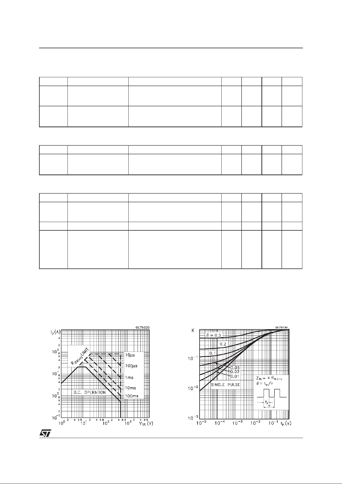
SafeOperating Area ThermalImpedance
3/8

IRFP460
OutputCharacteristics
Transconductance
TransferCharacteristics
Static Drain-sourceOn Resistance
Gate Charge vs Gate-sourceVoltage
4/8
CapacitanceVariations

IRFP460
Normalized Gate ThresholdVoltage vs
Source-drainDiode Forward Characteristics
Normalized On Resistance vsTemperature
5/8

IRFP460
Fig. 1: Unclamped InductiveLoad Test Circuit
Fig. 3: Switching Times Test CircuitsFor
ResistiveLoad
Fig. 1: Unclamped InductiveWaveform
Fig. 4: Gate Chargetest Circuit
Fig. 5: Test Circuit For InductiveLoad Switching
And Diode Recovery Times
6/8

TO-247 MECHANICAL DATA
IRFP460
DIM.
MIN. TYP. MAX. MIN. TYP. MAX.
A 4.7 5.3 0.185 0.209
D 2.2 2.6 0.087 0.102
E 0.4 0.8 0.016 0.031
F 1 1.4 0.039 0.055
F3 2 2.4 0.079 0.094
F4 3 3.4 0.118 0.134
G 10.9 0.429
H 15.3 15.9 0.602 0.626
L 19.7 20.3 0.776 0.779
L3 14.2 14.8 0.559 0.413 0.582
L4 34.6 1.362
L5 5.5 0.217
M 2 3 0.079 0.118
Dia 3.55 3.65 0.140 0.144
mm inch
P025P
7/8

IRFP460
Information furnishedis believed to be accurate and reliable. However, STMicroelectronics assumes no responsibility forthe consequences
of use of such information nor for any infringement ofpatents or other rights of third parties which may result from its use. No license is
granted by implication or otherwise under any patent or patent rights of STMicroelectronics. Specification mentioned in this publication are
subject to change without notice. This publication supersedes and replaces all information previously supplied. STMicroelectronics products
are not authorized for use as critical components inlife support devices or systems without express written approval ofSTMicroelectronics.
The ST logo is a registered trademark of STMicroelectronics
1998 STMicroelectronics – Printed inItaly –All Rights Reserved
STMicroelectronics GROUP OF COMPANIES
Australia - Brazil - Canada - China -France - Germany - Italy - Japan - Korea - Malaysia - Malta - Mexico - Morocco - TheNetherlands -
8/8
Singapore - Spain - Sweden - Switzerland - Taiwan - Thailand - United Kingdom - U.S.A.
.
 Loading...