

IRFBC30
N - CHANNEL600V - 1.8 Ω - 3.6A - TO-220
TYPE V
DSS
R
DS(on)
I
D
IRFBC30 600 V < 2.2 Ω 3.6 A
■ TYPICALR
■ EXTREMELY HIGH dv/dtCAPABILITY
■ 100%AVALANCHETESTED
■ VERYLOW INTRINSIC CAPACITANCES
■ GATECHARGE MINIMIZED
DS(on)
= 1.8 Ω
DESCRIPTION
The PowerMESH ΙΙ is the evolution of the first
generation of MESH OVERLAY. The layout
refinements introduced greatly improve the
Ron*areafigure of merit while keeping the device
at the leading edge for what concerns switching
speed,gate charge and ruggedness.
APPLICATIONS
■ HIGHCURRENT, HIGH SPEED SWITCHING
■ SWITHMODE POWER SUPPLIES (SMPS)
■ DC-AC CONVERTERS FOR WELDING
EQUIPMENTAND UNINTERRUPTIBLE
POWERSUPPLIESAND MOTORDRIVER
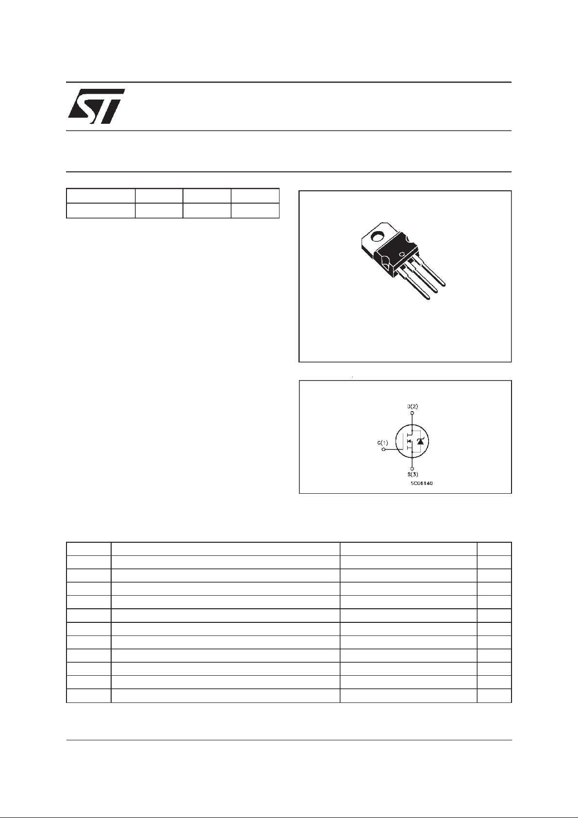
PowerMESH
ΙΙ MOSFET
2
1
TO-220
INTERNAL SCHEMATIC DIAGRAM
3
ABSOLUTE MAXIMUM RATINGS
Symbol Parameter Value Unit
V
V
V
I
DM
P
dv/ dt(
T
(•) Pulse width limited by safeoperating area (1)ISD≤3.6 A,di/dt ≤ 60 A/µs, VDD≤ V
January 2000
Drain-source Voltage (VGS=0) 600 V
DS
Dra in- g at e V oltage (RGS=20kΩ)
DGR
Gate -sourc e Voltage
GS
Drain Current (co ntinuous) a t Tc=25oC3.6A
I
D
Drain Current (co ntinuous) a t Tc=100oC2.3A
I
D
600 V
20 V
±
(•) Drain Current (pulsed) 14 A
Total Dissipation at Tc=25oC75W
tot
Derating Factor 0.6 W/
1) P eak Diode Recovery volt age slope 3 V/ns
St orage Te m pe r ature -65 to 150
stg
Max. O pera t ing Junc t io n Tempe rat u r e 150
T
j
,Tj≤T
(BR)DSS
JMAX
o
C
o
C
o
C
1/8
IRFBC30
THERMAL DATA
R
thj-case
Rthj-a mb
R
thc-sink
T
AVALANCHE CHARACTERISTICS
Symbol Para meter Max Value Uni t
I
AR
E
Ther mal Resist ance Junction-cas e Max
Ther mal Resist ance Junction-amb ien t Max
Thermal Resistance Case-sink Typ
Maximum Lead Temper at u r e F or S old er ing Purp ose
l
Avalanche Current, Re petitiv e or No t - Re petitiv e
(pulse width l imited by T
Single Pulse Avalanche Energy
AS
(starting T
=25oC, ID=IAR,VDD=50V)
j
max)
j
1.7
62.5
0.5
300
3.6 A
300 mJ
o
C/W
oC/W
o
C/W
o
C
ELECTRICAL CHARACTERISTICS (T
=25oC unless otherwisespecified)
case
OFF
Symbol Parameter Test Condit ions Min. Typ. Max. Unit
V
(BR)DSS
Drain-sou rce
=250µAVGS=0
I
D
600 V
Break d own Vo lt age
I
DSS
I
GSS
Zero Gate Voltage
Drain Curr ent (V
GS
Gat e- b ody Leaka ge
Current ( V
DS
=0)
=0)
V
=MaxRating
DS
= Max Rating Tc=125oC
V
DS
= ± 20 V
V
GS
1
50
± 100 nA
ON(∗)
Symbol Parameter Test Condit ions Min. Typ. Max. Unit
V
GS(th)
Gate Threshold
V
DS=VGSID
= 250 µ A
234V
Voltage
R
DS(on)
Static Drain-source On
VGS=10V ID= 2.2 A 1.8 2. 2
Resistanc e
I
D(on)
On St ate Dra in Current VDS>I
D(on)xRDS(on)max
3.6 A
VGS=10V
DYNAMIC
Symbol Parameter Test Condit ions Min. Typ. Max. Unit
g
(∗)Forward
fs
Tr ansconduc tanc e
C
C
C
Input Capacitan ce
iss
Out put Capac itance
oss
Reverse T ransf er
rss
Capacitance
VDS>I
D(on)xRDS(on)maxID
=2.2A 2.5 S
VDS=25V f=1MHz VGS=0 475
72
10
µA
µ
Ω
pF
pF
pF
A
2/8
IRFBC30
ELECTRICAL CHARACTERISTICS
(continued)
SWITCHING ON
Symbol Parameter Test Condit ions Min. Typ. Max. Unit
t
d(on)
Turn-on Time
r
Rise T im e
t
VDD= 250 V ID=2.5A
R
=4.7
G
Ω
VGS=10V
14
14
(see test circu it, figure 3)
Q
Q
Q
Total Gate Charge
g
Gat e- Source Charge
gs
Gate-Drain Charge
gd
VDD= 480 V ID=3.6AVGS=10V 16.5
2.5
9
23.1 nC
SWITCHING OFF
Symbol Parameter Test Condit ions Min. Typ. Max. Unit
t
r(Voff)
t
t
Off -voltage Rise Ti me
Fall Time
f
Cross-ov er Ti me
c
VDD= 480 V ID=3.6A
=4.7 ΩVGS=10V
R
G
(see test circu it, figure 5)
15
19
24
SOURCEDRAINDIODE
Symbol Parameter Test Condit ions Min. Typ. Max. Unit
I
SD
I
SDM
V
SD
t
Q
I
RRM
(∗) Pulsed: Pulse duration = 300 µs, duty cycle 1.5 %
(•) Pulse width limited by safe operatingarea
Source-drain Current
(•)
Source-drain Current
3.6
14
(pulsed)
(∗) Forwar d On Voltage ISD=3.6A VGS=0 1.6 V
Reverse R ec o very
rr
Time
Reverse R ec o very
rr
= 5 A di/dt = 100 A /µs
I
SD
= 100 V Tj=150oC
V
DD
(see test circu it, figure 5)
600
2.8
Charge
Reverse R ec o very
9
Current
ns
ns
nC
nC
ns
ns
ns
A
A
ns
µ
A
C
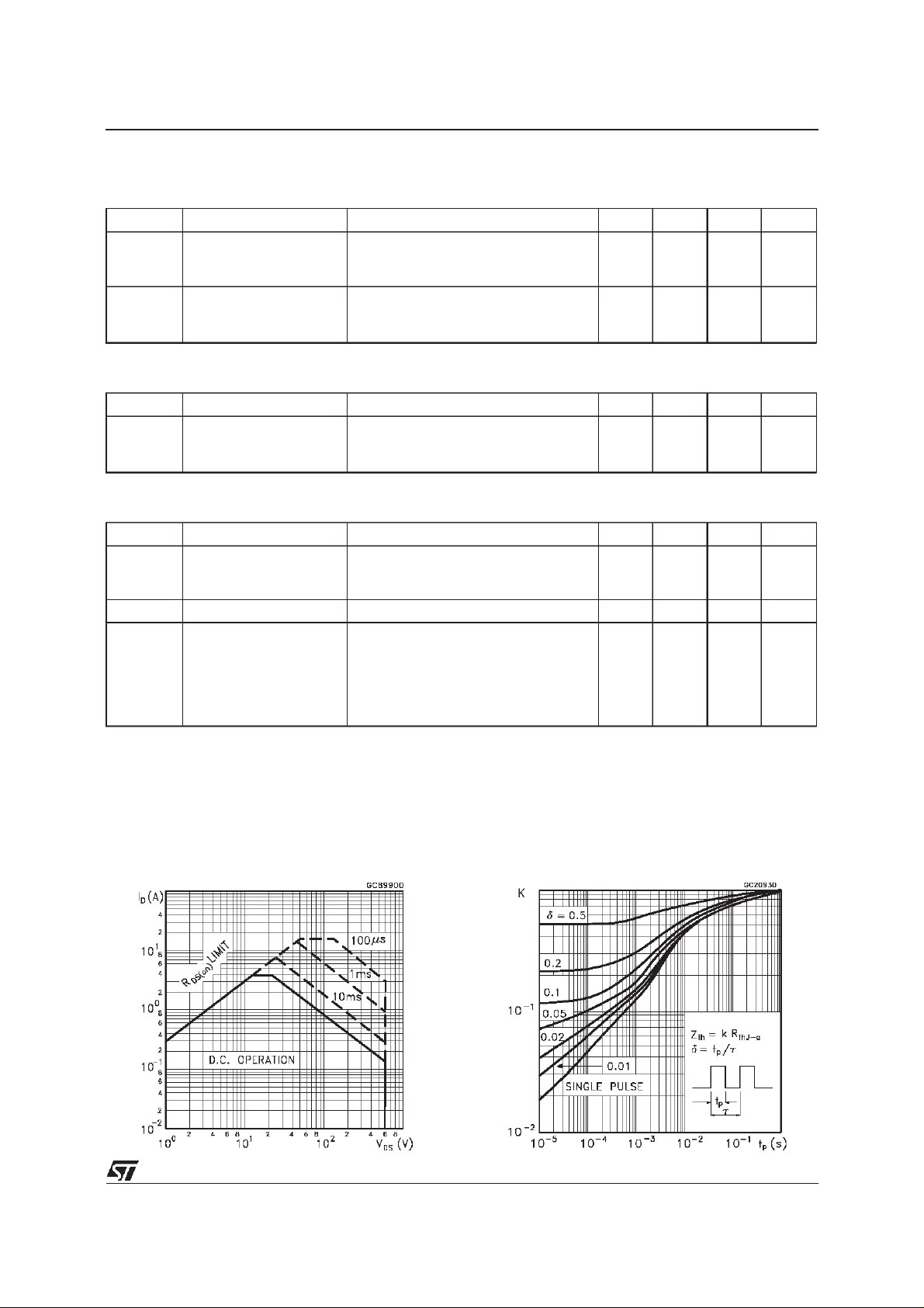
SafeOperating Area ThermalImpedance
3/8
 Loading...