

SGS Thomson Microelectronics IRF830 Datasheet
IRF830
N - CHANNEL 500V - 1.35Ω - 4.5A - TO-220
PowerMESH MOSFET
TYPE V
DSS
R
DS(on)
I
D
IRF830 500 V < 1.5 Ω 4.5 A
■ TYPICALR
■ EXTREMELY HIGHdv/dt CAPABILITY
■ 100% AVALANCHETESTED
■ VERYLOW INTRINSIC CAPACITANCES
■ GATECHARGEMINIMIZED
DS(on)
=1.35 Ω
DESCRIPTION
This power MOSFET is designed using the
company’sconsolidated strip layout-basedMESH
OVERLAY process. This technology matches
and improves the performances compared with
standardparts from various sources.
APPLICATIONS
■ HIGH CURRENT, HIGHSPEEDSWITCHING
■ SWITHMODE POWER SUPPLIES (SMPS)
■ DC-ACCONVERTERS FOR WELDING
EQUIPMENTAND UNINTERRUPTIBLE
POWERSUPPLIES AND MOTORDRIVER
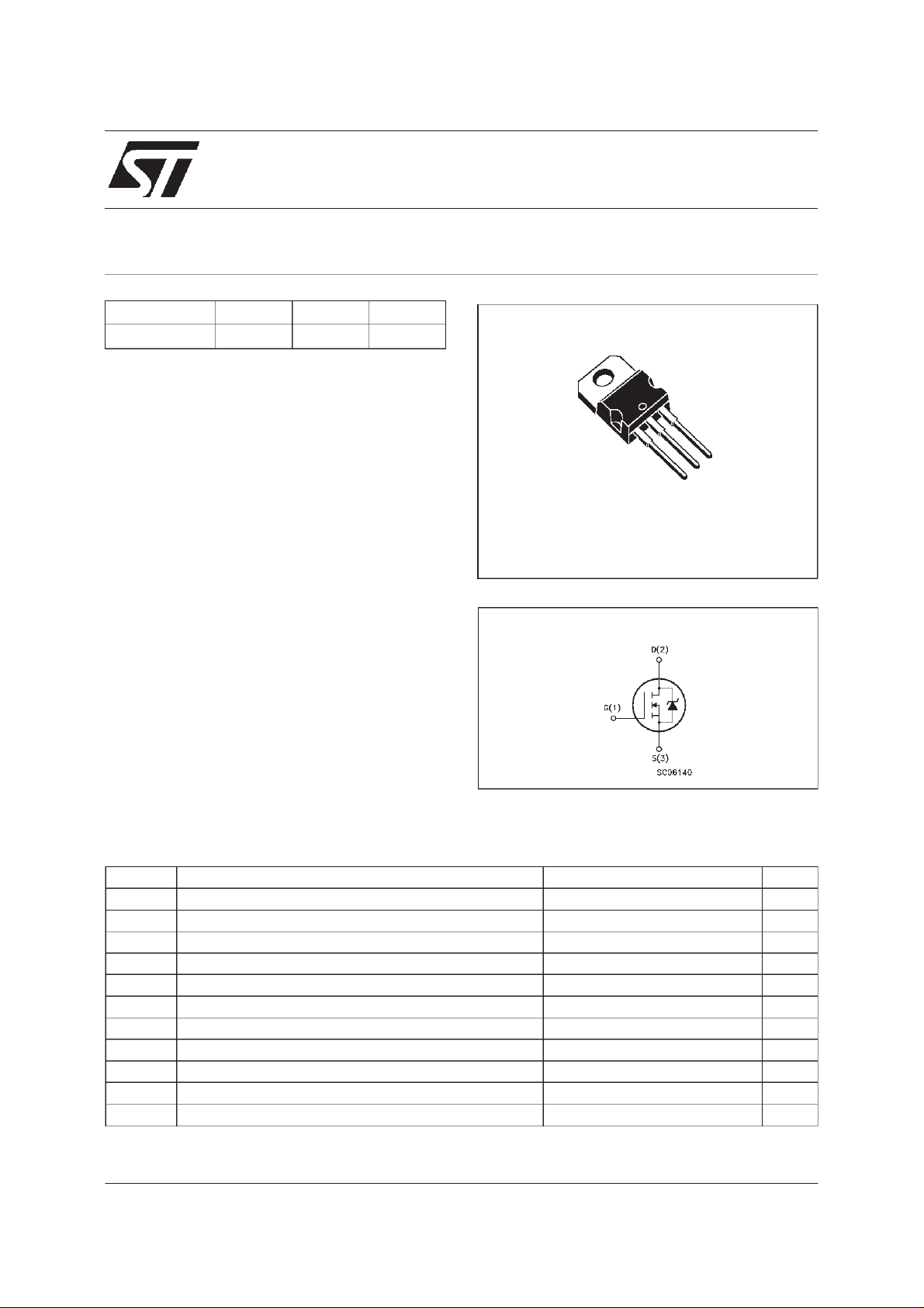
3
2
1
TO-220
INTERNAL SCHEMATIC DIAGRAM
ABSOLUTE MAXIMUM RATINGS
Symb o l Para meter Value Uni t
V
V
V
I
DM
P
dv/dt(
T
(•) Pulsewidth limitedby safe operatingarea (1)ISD≤ 4.5A, di/dt ≤ 75 A/µs,VDD≤ V
First Digitof the Datecode Being Z or K IdentifiesSilicon Characterized in this Datasheet
August 1998
Drain-source Voltage (VGS=0) 500 V
DS
Drain- gate Voltage (RGS=20kΩ)
DGR
Gat e- source Voltage ± 20 V
GS
Drain Current (cont in uous) at Tc=25oC4.5A
I
D
Drain Current (cont in uous) at Tc=100oC2.9A
I
D
500 V
(•) Drain Current (pulsed ) 18 A
Tot al Dissipat i on at Tc=25oC100W
tot
Derating Factor 0.8 W/
1) Peak Di ode Recovery voltage slope 3.5 V/ns
Sto rage T em pe rature -65 to 150
stg
Max. Operat in g Junct io n Temper at u r e 150
T
j
,Tj≤T
(BR)DSS
JMAX
o
C
o
C
o
C
1/8
IRF830
THERMAL DATA
R
thj-case
Rthj-amb
R
thc-sin k
T
AVALANCHE CHARACTERISTICS
Symbol Para met e r Max Va lu e Unit
I
AR
E
Ther mal Resistanc e Junction-case Max
Ther mal Resistanc e Junction-ambie nt Max
Ther mal Resistanc e Case-si nk T yp
Maximum Lead Te mperature F or Soldering Pur p os e
l
Avalanche Current , Repet it i ve or Not-Repetitive
(pulse w idth limited by T
Single Pulse Avalanche Energy
AS
(starting T
=25oC, ID=IAR,VDD=50V)
j
max)
j
1.25
62.5
0.5
300
4.5 A
290 mJ
o
C/W
oC/W
o
C/W
o
C
ELECTRICAL CHARACTERISTICS (T
=25oC unlessotherwise specified)
case
OFF
Symbol Parameter Test Condition s Min. Typ. Max. Unit
V
(BR)DSS
Drain-source
=250µAVGS=0
I
D
500 V
Breakdown Volt age
I
DSS
I
GSS
Zer o Gate Vo lt age
Drain Curre nt (V
GS
Gat e-body Leakage
Current (V
DS
=0)
=0)
V
=MaxRating
DS
=MaxRating Tc=125oC
V
DS
= ± 20 V
V
GS
1
50
± 100 nA
ON (∗)
Symbol Parameter Test Condition s Min. Typ. Max. Unit
V
GS(th )
Gate Threshold
V
DS=VGSID
=250µA
234V
Voltage
R
DS(on)
Stati c Drain-so urce On
VGS=10V ID= 2.7 A 1.35 1.5 Ω
Resistance
I
D(on)
On S tate Drain Cur rent VDS>I
D(on)xRDS(on)max
4.5 A
VGS=10V
DYNAMIC
Symbol Parameter Test Condition s Min. Typ. Max. Unit
g
(∗)Forward
fs
Tr ansconductance
C
C
C
Input Capacit ance
iss
Out put Capa citance
oss
Reverse Transfer
rss
Capa cit an c e
VDS>I
D(on)xRDS(on)maxID
=2.7A 2.5 S
VDS=25V f=1MHz VGS= 0 610
120
10
µA
µA
pF
pF
pF
2/8
IRF830
ELECTRICAL CHARACTERISTICS (continued)
SWITCHINGON
Symbol Parameter Test Condition s Min. Typ. Max. Unit
t
d(on)
t
r
Turn-on Time
Rise Time
VDD=250V ID=2.9A
=4.7 Ω VGS=10V
R
G
(see test circuit, figure 3)
Q
Q
Q
Total Gate Charge
g
Gat e-Source Charge
gs
Gate-Drain Charge
gd
VDD=400V ID=3A VGS=10V 22
SWITCHINGOFF
Symbol Parameter Test Condition s Min. Typ. Max. Unit
t
r(Voff)
t
Of f - voltage Rise Tim e
t
Fall Time
f
Cross-over Tim e
c
VDD=400V ID=4.5A
=4.7 Ω VGS=10V
R
G
(see test circuit, figure 5)
SOURCE DRAIN DIODE
Symbol Parameter Test Condition s Min. Typ. Max. Unit
I
SD
I
SDM
V
SD
t
Q
I
RRM
(∗) Pulsed: Pulse duration =300 µs, duty cycle 1.5 %
(•) Pulse width limited by safeoperating area
Source-drain Cu rrent
(•)
Source-drain Cu rrent
(pulsed)
(∗) For ward O n V o lt age ISD=4.5A VGS=0 1.6 V
Reverse Recovery
rr
Time
Reverse Recovery
rr
= 4.5 A di/dt = 100 A/µs
I
SD
=100V Tj=150oC
V
DD
(see test circuit, figure 5)
Charge
Reverse Recovery
Current
11.5
8
30 nC
7.2
8
7
5
15
4.5
18
435
3.3
15
ns
ns
nC
nC
ns
ns
ns
A
A
ns
µC
A
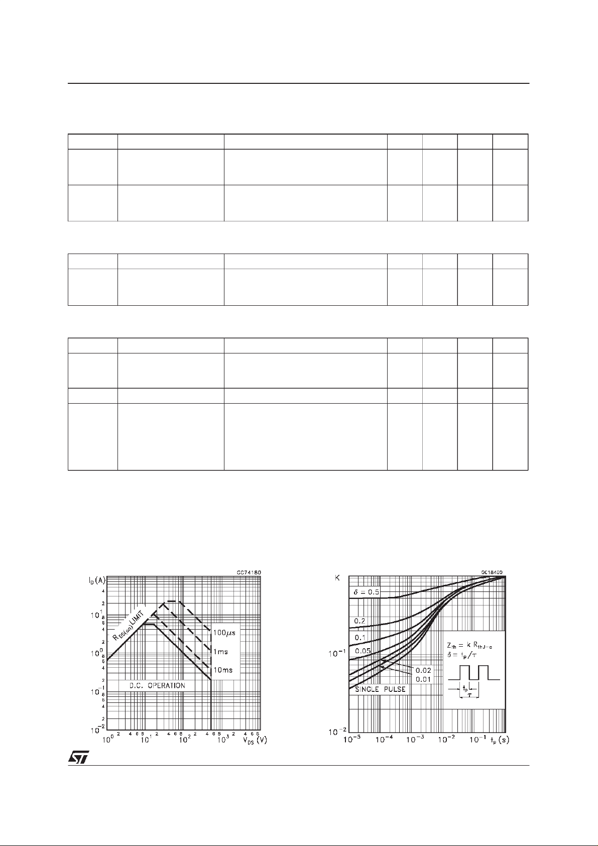
Safe Operating Area ThermalImpedance
3/8
 Loading...