

IRF640S
N - CHANNEL200V - 0.150Ω - 18A TO-263
MESH OVERLAY MOSFET
TYPE V
DSS
R
DS(on)
I
D
IRF 640S 200 V < 0. 18 Ω 18 A
■ TYPICALR
■ EXTREMELYHIGH dv/dt CAPABILITY
■ VERYLOW INTRINSIC CAPACITANCES
■ GATECHARGE MINIMIZED
DS(on)
= 0.150 Ω
DESCRIPTION
This power MOSFET is designed using he
company’sconsolidatedstrip layout-based MESH
OVERLAY process. This technology matches
and improves the performances compared with
standardpartsfrom various sources.
APPLICATIONS
■ HIGHCURRENT SWITCHING
■ UNINTERRUPTIBLE POWERSUPPLY(UPS)
■ DC/DC COVERTERSFOR TELECOM,
INDUSTRIAL,AND LIGHTING EQUIPMENT.
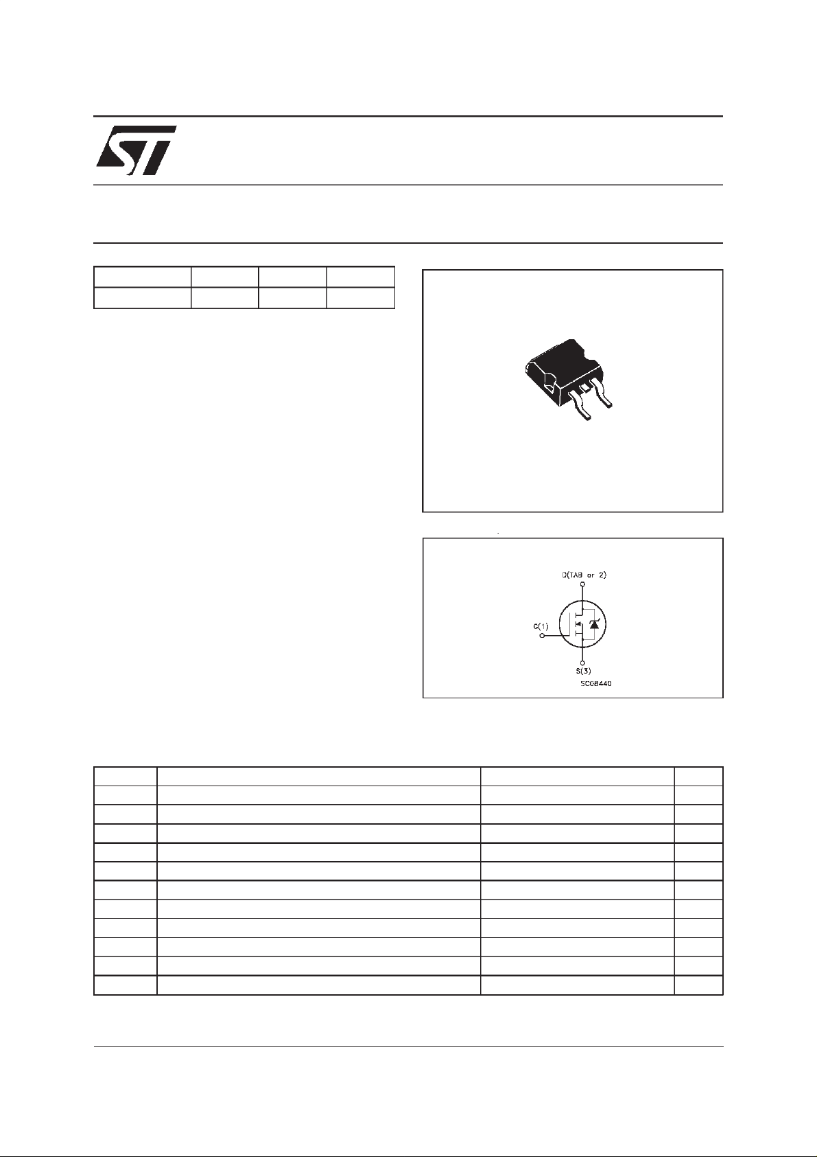
3
1
D2PAK
TO-263
(suffix ”T4”)
INTERNAL SCHEMATIC DIAGRAM
ABSOLUTE MAXIMUM RATINGS
Symbol Parameter Value Unit
V
V
V
I
DM
P
dv/dt(
T
(•) Pulse width limited by safeoperating area (1)ISD≤ 18A, di/dt ≤ 300A/µs,VDD≤ V
September 1999
Dra in- sour c e Voltage (VGS= 0) 200 V
DS
Dra in- gate Volt age (RGS=20kΩ) 200 V
DGR
Gat e-source V oltage ± 20 V
GS
Dra in Current (c ont inuous) a t Tc=25oC18A
I
D
Dra in Current (c ont inuous) a t Tc=100oC11A
I
D
(•) Dra in Current (p ulsed) 72 A
Tot al Dissipation at Tc=25oC 125 W
tot
Der ati ng Factor 1.0 W/
1) Peak Diode Re c overy volt age s l ope 5 V/ns
St orage Tempe r ature -65 t o 150
stg
Max. O perating Junction T em perature 150
T
j
,Tj≤T
(BR)DSS
JMAX
o
C
o
C
o
C
1/8
IRF640S
THERMAL DATA
3.12
R
thj-case
R
thj-amb
R
thc-sink
T
AVALANCHE CHARACTERISTICS
Symbol Parameter Max Value Unit
I
AR
E
Ther mal Resistanc e Junct ion-case Max
Ther mal Resistanc e Junct ion-ambient Max
Ther mal Resistanc e Case-sink Ty p
Maximum Lead Te mperature For Solder ing Purp os e
l
Avalanche Current, Repetitive or Not-Repetitive
(pulse width limited by T
Single P ul s e Avalanc he Energy
AS
(starting T
=25oC, ID=IAR,VDD=50V)
j
max)
j
1.0
62.5
0.5
300
18 A
280 mJ
o
C/W
oC/W
o
C/W
o
C
ELECTRICAL CHARACTERISTICS (T
=25oC unless otherwisespecified)
case
OFF
Symbol Parameter Test Condit ions Min. Typ. Max. Unit
V
(BR)DSS
Drain-source
ID=250µAVGS= 0 200 V
Break dow n Volt age
I
DSS
I
GSS
Zero Gate Voltage
Drain Cur rent (V
GS
Gat e- bod y L eak ag e
Current (V
DS
=0)
=0)
=MaxRating
V
DS
V
=MaxRating Tc=125oC
DS
V
= ± 20 V ± 100 nA
GS
10
1
ON(∗)
Symbol Parameter Test Condit ions Min. Typ. Max. Unit
V
GS(th)
R
DS(on)
Gate Threshold Voltage VDS=VGSID= 250µA 234V
Sta t ic Drain -s ource On
VGS=10V ID= 9 A 0.15 0.18 Ω
Resistance
I
D(on)
On State Drain Current VDS>I
D(on)xRDS(on)max
18 A
VGS=10V
DYNAMIC
Symbol Parameter Test Condit ions Min. Typ. Max. Unit
g
(∗)Forward
fs
Tr ansc on duc tance
C
C
C
Input Capac i t ance
iss
Out put Capacitanc e
oss
Reverse Tr ansfer
rss
Capacit a nc e
VDS>I
D(on)xRDS(on)maxID
=9A 3 4 S
VDS=25V f=1MHz VGS= 0 1200
200
60
1560
260
80
µA
µ
pF
pF
pF
A
2/8
IRF640S
ELECTRICAL CHARACTERISTICS
(continued)
SWITCHINGON
Symbol Parameter Test Condit ions Min. Typ. Max. Unit
t
d(on)
t
r
Turn-on Time
Rise Ti m e
VDD=100V ID=9A
R
=4.7
G
Ω
VGS=10V
13
27
17
35
(see test circuit, figure 3)
Q
Q
Q
Tot al Gat e Charge
g
Gat e- Source Charg e
gs
Gate-Drain Charge
gd
VDD= 160 V ID=18A VGS= 10V 55
10
21
72 nC
SWITCHINGOFF
Symbol Parameter Test Condit ions Min. Typ. Max. Unit
t
r(Voff)
t
t
Off-voltage Rise Time
Fall T ime
f
Cross-over T ime
c
VDD=160V ID=18A
=4.7 Ω VGS=10V
R
G
(see test circuit, figure 5)
21
25
50
27
32
65
SOURCEDRAINDIODE
Symbol Parameter Test Condit ions Min. Typ. Max. Unit
I
SD
I
SDM
V
SD
t
Q
I
RRM
(∗) Pulsed:Pulse duration = 300µs, duty cycle 1.5%
(•) Pulse width limited by safe operating area
Source-drain Current
(•)
Source-drain Current
18
72
(pulsed)
(∗)ForwardOnVoltage ISD=18A VGS=0 1.5 V
Reverse Recovery
rr
Time
Reverse Recovery
rr
ISD= 18 A di/dt = 100 A /µs
=50V Tj= 150oC
V
DD
(see test circuit, figure 5)
240
1.8
Charge
Reverse Recovery
15
Current
ns
ns
nC
nC
ns
ns
ns
A
A
ns
µ
A
C
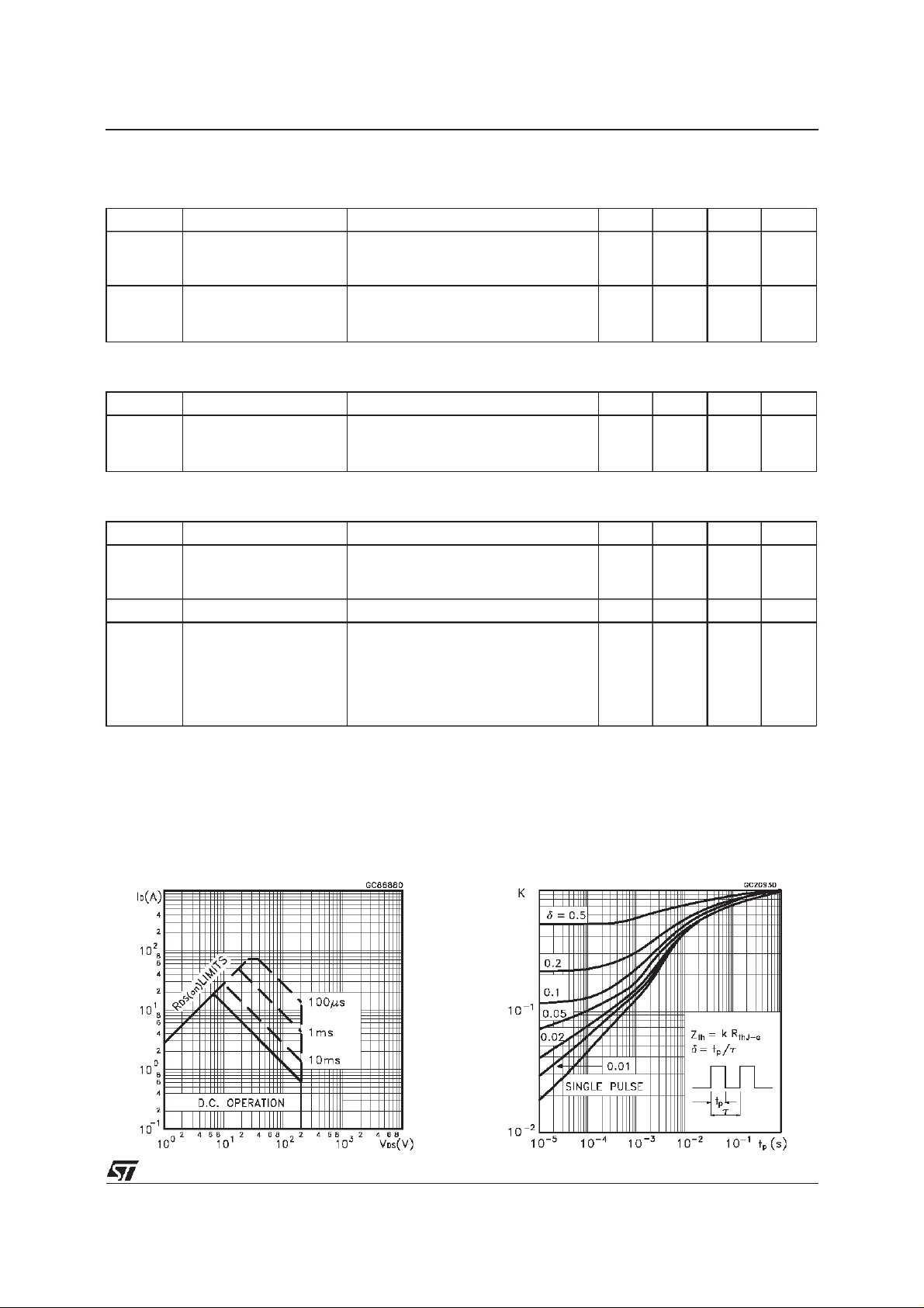
SafeOperating Area ThermalImpedance
3/8
 Loading...